Downloaded 2,668 times
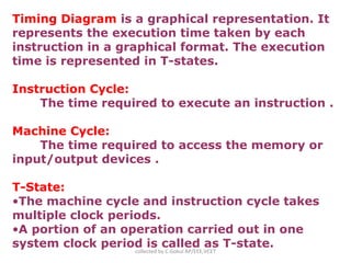
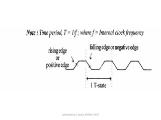
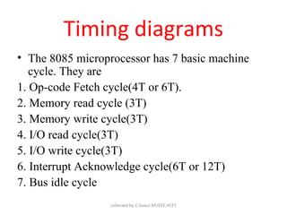
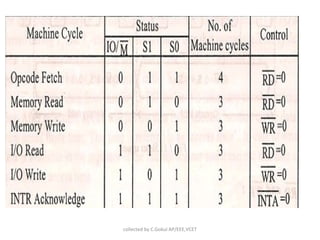
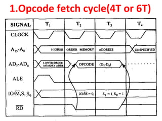
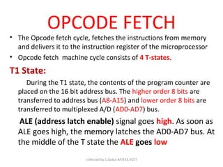
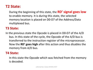
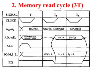
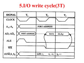
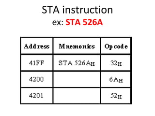
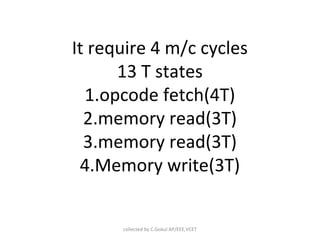
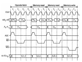

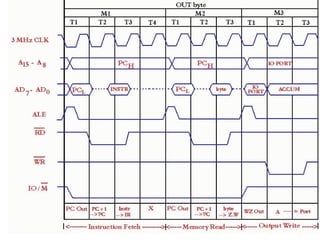
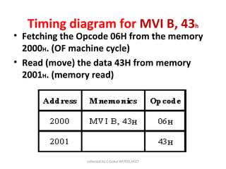
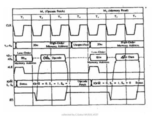
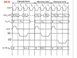
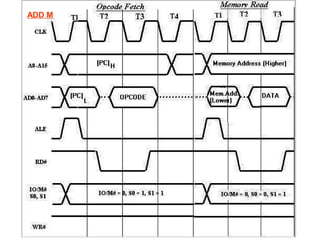
The document discusses the timing diagram of the 8085 microprocessor. It explains that a timing diagram is a graphical representation of the execution time of each instruction. It then describes the different machine cycles of the 8085 including the opcode fetch cycle, memory read cycle, memory write cycle, I/O read cycle, I/O write cycle, and interrupt acknowledge cycle. It provides details on the T-states within each machine cycle and examples of timing diagrams for different instructions like STA, IN, OUT, MVI, INR and ADD. Finally, it lists several references used to collect information on the 8085 timing diagram.