Downloaded 179 times
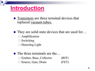
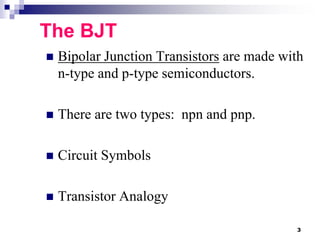
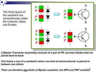
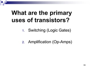
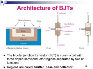
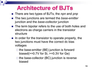
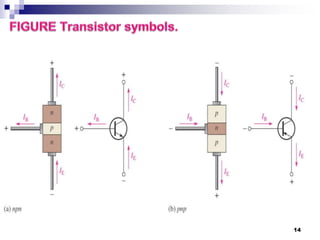
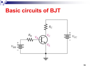
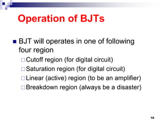


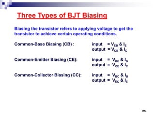
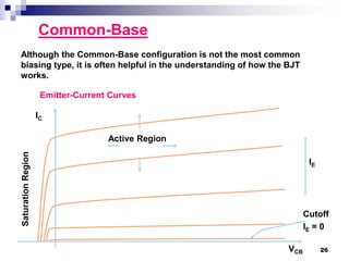

1. The document discusses bipolar junction transistors (BJTs), including their construction, operation, and uses. BJTs are made of n-type and p-type semiconductors and have three terminals - emitter, base, and collector. 2. There are two types of BJTs - npn and pnp. BJTs operate in different regions including cutoff, saturation, linear/active, and breakdown. Key equations relate currents and voltages at the terminals. 3. BJTs are used for amplification, switching, and detecting light. They can be configured in common-emitter, common-base, or common-collector circuits and operated in classes A or B for


