Downloaded 253 times
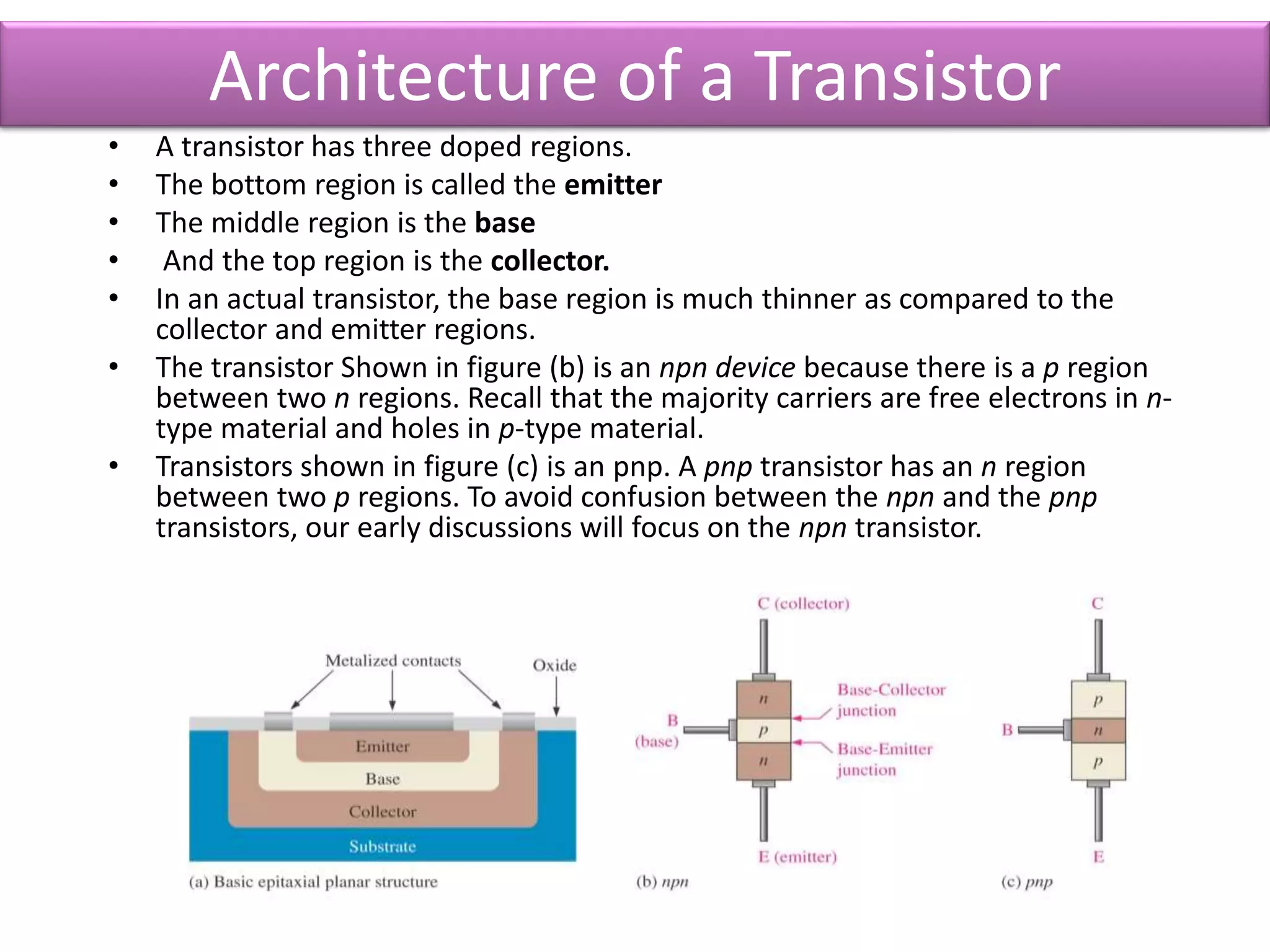


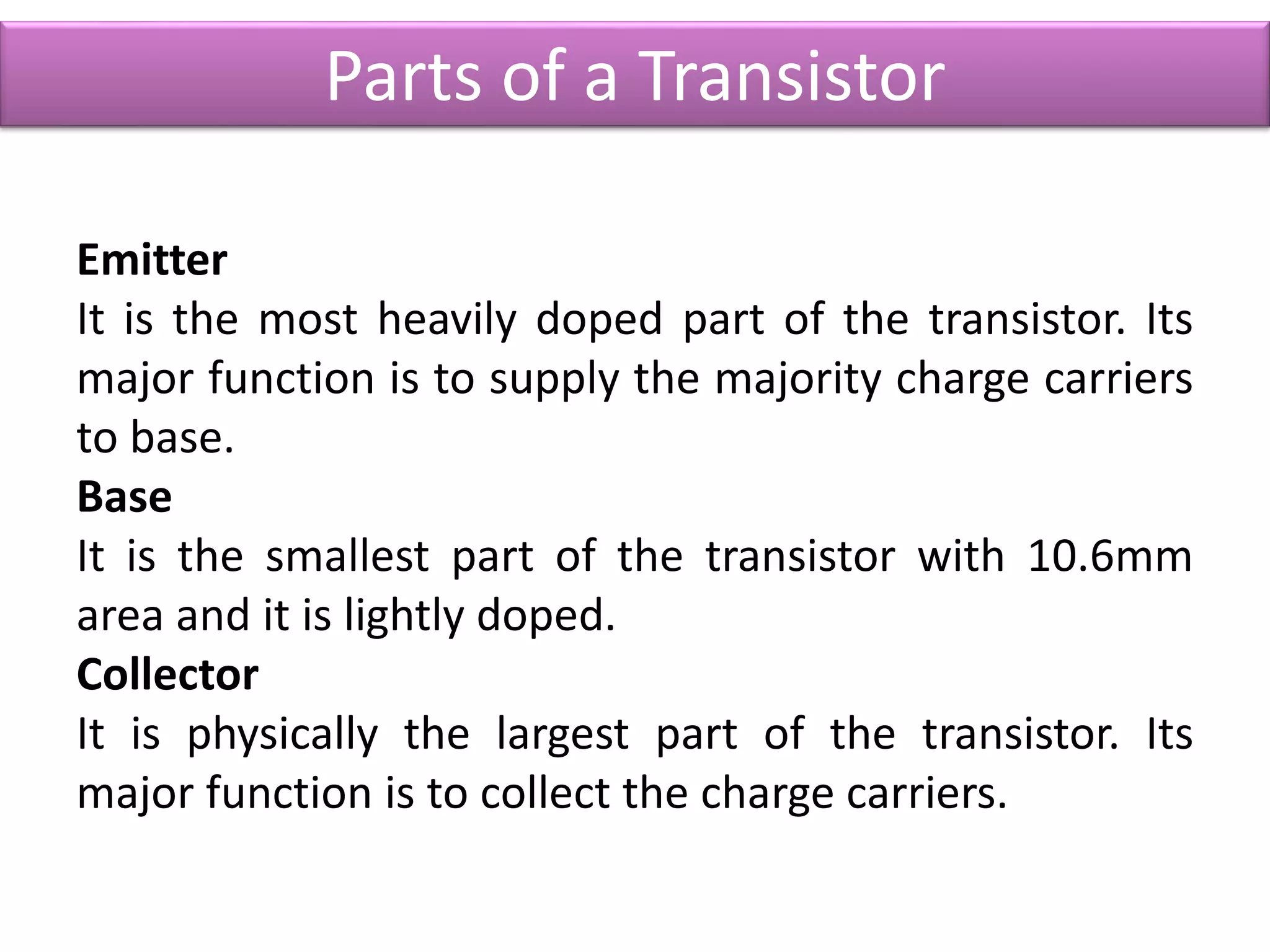


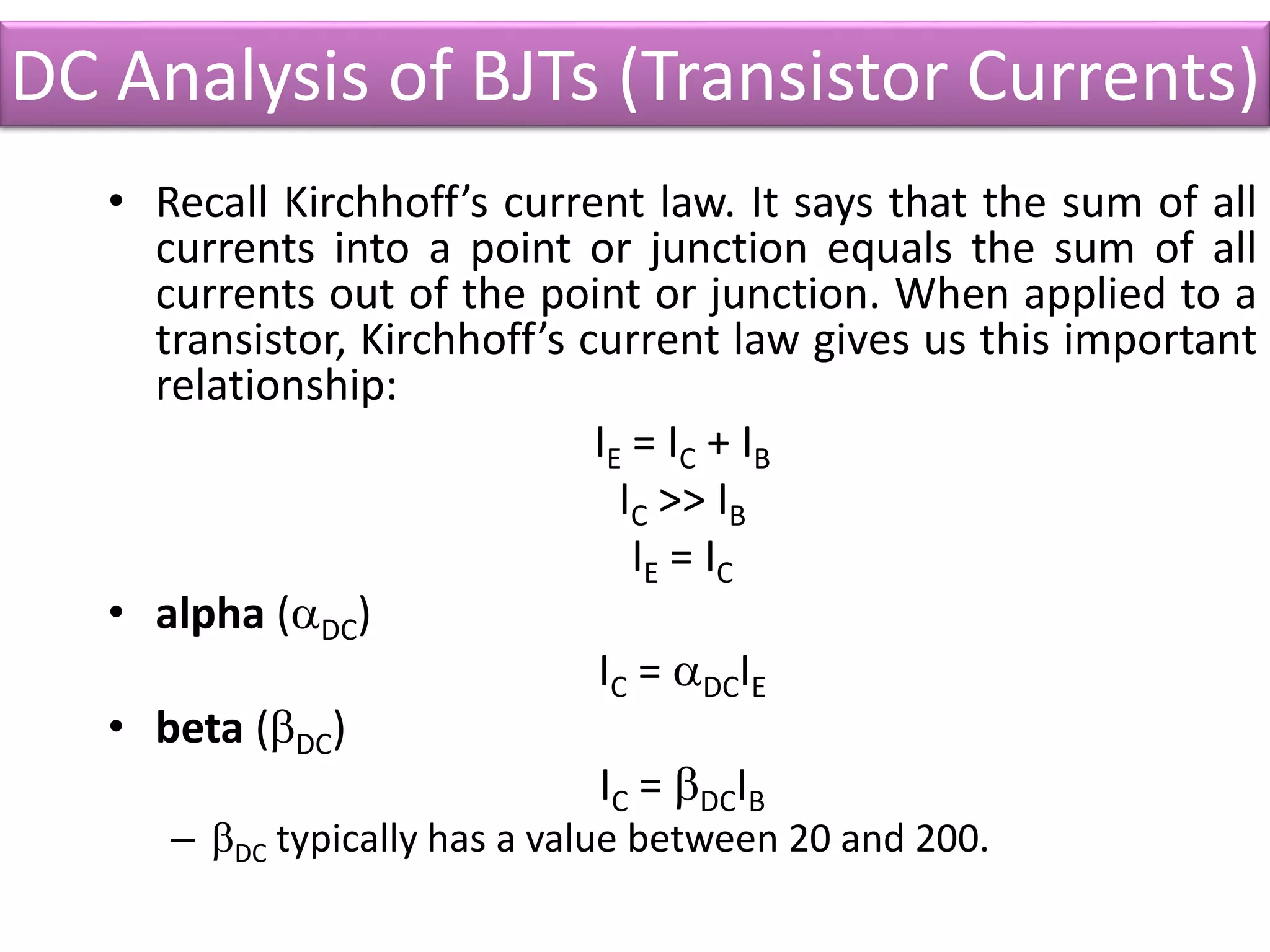


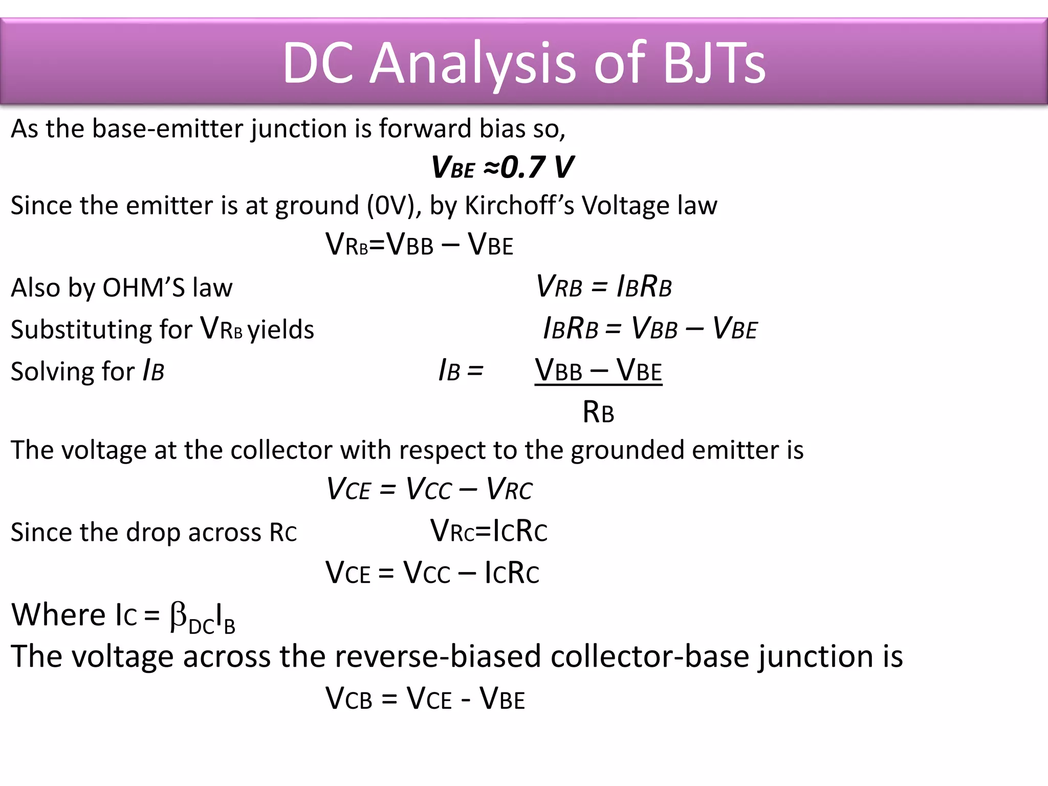


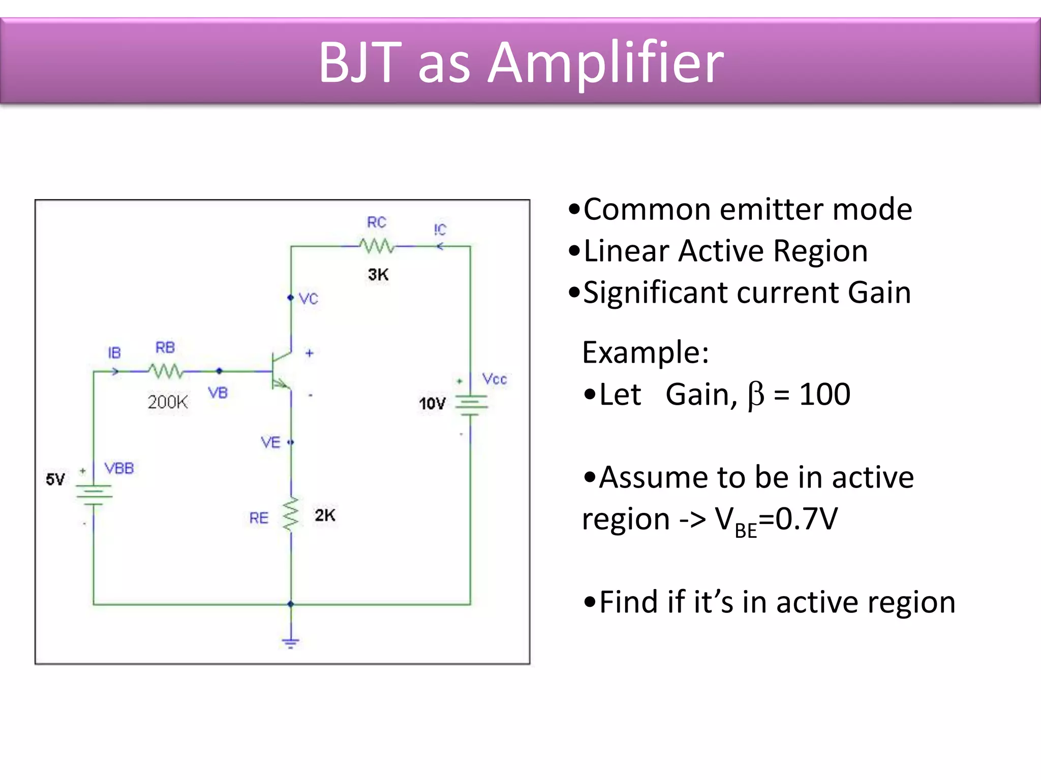
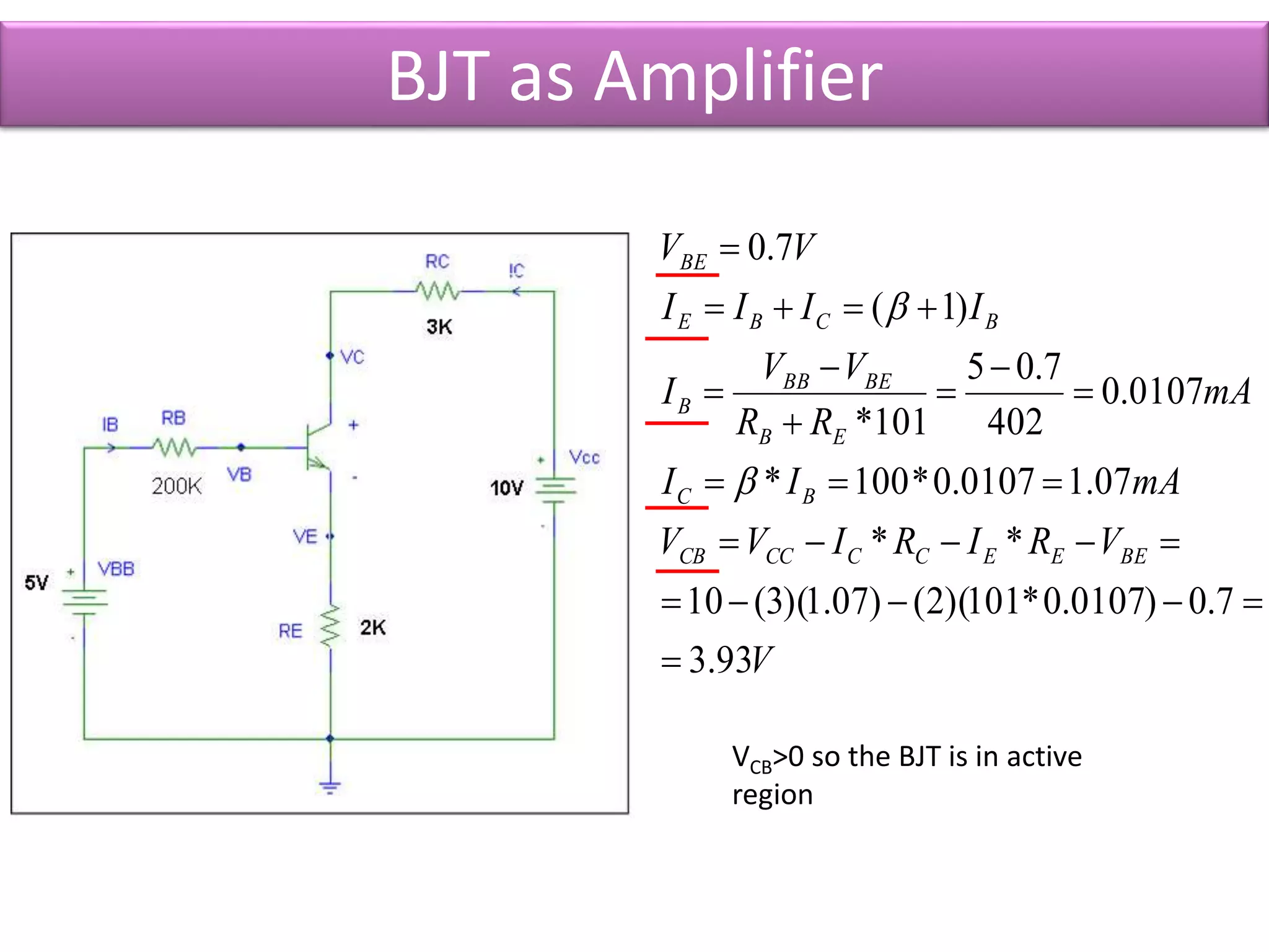

The document discusses bipolar junction transistors (BJTs). It describes the basic construction of an NPN and PNP transistor including the emitter, base, and collector regions. It explains that the base-emitter junction must be forward biased and the base-collector junction must be reverse biased for the transistor to operate properly. The document also discusses BJT biasing circuits, operating regions including cutoff, saturation, and active modes, and uses of BJTs as switches and amplifiers.


![ict_presentation_final_final_final[1].pptx](https://cdn.slidesharecdn.com/ss_thumbnails/ictpresentationfinalfinalfinal1-251230145259-2b4839bd-thumbnail.jpg?width=640&height=640&fit=bounds)


