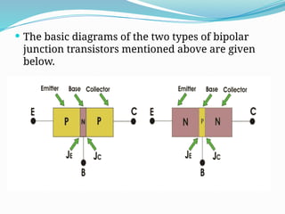
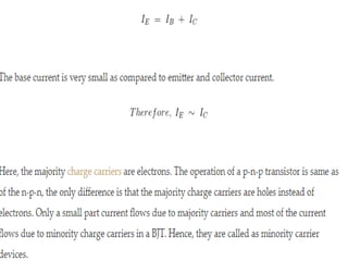
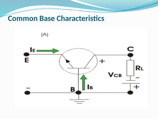
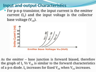
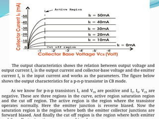
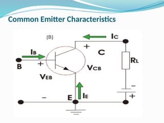
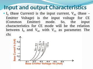
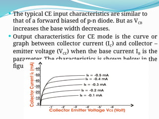
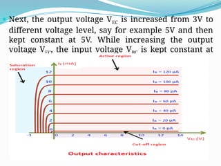
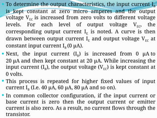
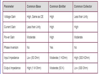
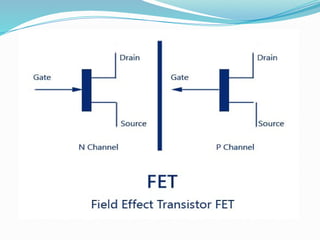
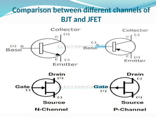
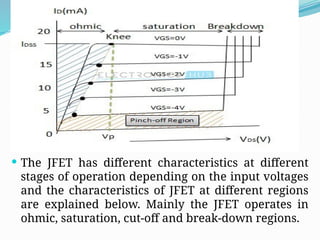
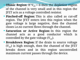
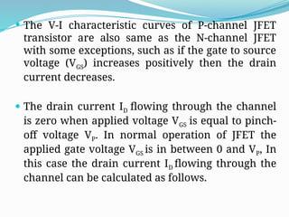
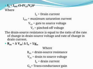
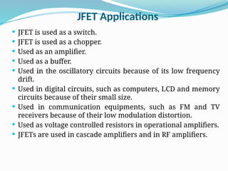
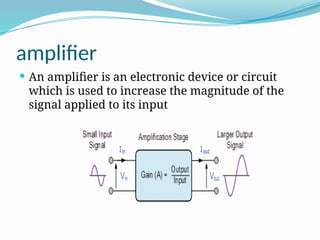
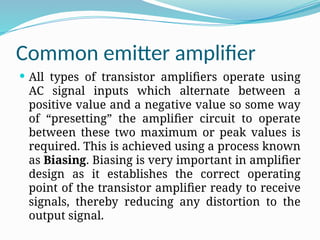
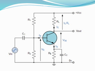
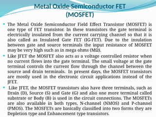
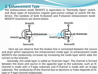
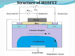
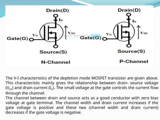
Bipolar Junction Transistor or BJT
 The word transistor is derived from the words
“Transfer” and “Resistor” it describes the operation
of a BJT i.e. the transfer of an input signal from a
low resistance circuit to a high resistance circuit.
This type of transistor is made up of
semiconductors.
 Transistors are used in the construction of
Integrated Circuits (ICs). The number of transistors
that we have been able to fit into an IC has rapidly
increased since their creation.
Definition of BJT
 A bipolar junction transistor is a three terminal
semiconductor device consisting of two p-n junctions
which is able to amplify or magnify a signal. It is a
current controlled device.
 The three terminals of the BJT are the base, the
collector and the emitter. A signal of small amplitude
if applied to the base is available in the amplified
form at the collector of the transistor.
 This is the amplification provided by the BJT. Note
that it does require an external source of DC power
supply to carry out the amplification process.
 The basic diagrams of the two types of bipolar
junction transistors mentioned above are given
below.
 From the above figure, we can see that every BJT
has three parts named emitter, base and collector.
JE and JC represent junction of emitter and junction
of collector respectively. Now initially it is
sufficient for us to know that emitter based
junction is forward biased and collector base
junctions is reverse biased. The next topic will
describe the two types of this transistors.
 N-P-N Bipolar Junction Transistor
 P-N-P Bipolar Junction Transistor
N-P-N Bipolar Junction Transistor
 As started before in n-p-n bipolar transistor one
p-type semiconductor resides between two n-
type semiconductors the diagram below a n-p-n
transistor is shown
 Now IE, IC is emitter current and collect current
respectively and VEB and VCB are emitter base
voltage and collector base voltage respectively.
According to convention if for the emitter, base
and collector current IE, IB and IC current goes
into the transistor the sign of the current is taken
as positive and if current goes out from the
transistor then the sign is taken as negative. We
can tabulate the different currents and voltages
inside the n-p-n transistor.
P-N-P Bipolar Junction Transistor
 Similarly for p-n-p bipolar junction transistor a
n-type semiconductors is sandwiched between
two p-type semiconductors. The diagram of a p-n-p
transistor is shown below
 For p-n-p transistors, current enters into the
transistor through the emitter terminal. Like any
bipolar junction transistor, the emitter-base
junction is forward biased and the collector-base
junction is reverse biased. We can tabulate the
emitter, base and collector current, as well as the
emitter base, collector base and collector emitter
voltage for p-n-p transistors also.
Working Principle of BJT
 Figure shows an n-p-n transistor biased in the active region See
transistor biasing, the BE junction is forward biased whereas the CB
junction is reversed biased. The width of the depletion region of the
BE junction is small as compared to that of the CB junction. The
forward bias at the BE junction reduces the barrier potential and
causes the electrons to flow from the emitter to base. As the base is
thin and lightly doped it consists of very few holes so some of the
electrons from the emitter (about 2%) recombine with the holes
present in the base region and flow out of the base terminal. This
constitutes the base current, it flows due to recombination of
electrons and holes (Note that the direction of conventional current
flow is opposite to that of flow of electrons). The remaining large
number of electrons will cross the reverse biased collector junction to
constitute the collector current. Thus by KCL,
Bipolar Junction Transistors Characteristics
 The three parts of a BJT are collector, emitter and base.
Before knowing about the bipolar junction transistor
characteristics, we have to know about the modes of
operation for this type of transistors. The modes are
 Common Base (CB) mode
 Common Emitter (CE) mode
 Common Collecter (CC) mode
 Now coming to the characteristics of BJT there are different
characteristics for different modes of operation.
Characteristics is nothing but the graphical forms of
relationships among different current and voltage variables
of the transistor. The characteristics for p-n-p transistors are
given for different modes and different parameters.
Common Base Characteristics
Input and output Characteristics
 For p-n-p transistor, the input current is the emitter
current (IE) and the input voltage is the collector
base voltage (VCB).
As the emitter – base junction is forward biased, therefore
the graph of IE Vs VEB is similar to the forward characteristics
of a p-n diode. IE increases for fixed VEB when VCB increases.
The output characteristics shows the relation between output voltage and
output current IC is the output current and collector-base voltage and the emitter
current IE is the input current and works as the parameters. The figure below
shows the output characteristics for a p-n-p transistor in CB mode.
As we know for p-n-p transistors IE and VEB are positive and IC, IB, VCB are
negative. These are three regions in the curve, active region saturation region
and the cut off region. The active region is the region where the transistor
operates normally. Here the emitter junction is reverse biased. Now the
saturation region is the region where both the emitter collector junctions are
forward biased. And finally the cut off region is the region where both emitter
Common Emitter Characteristics
Input and output Characteristics
 IB (Base Current) is the input current, VBE (Base –
Emitter Voltage) is the input voltage for CE
(Common Emitter) mode. So, the input
characteristics for CE mode will be the relation
between IB and VBE with VCE as parameter. The
characteristics are shown below
 The typical CE input characteristics are similar to
that of a forward biased of p-n diode. But as VCB
increases the base width decreases.
 Output characteristics for CE mode is the curve or
graph between collector current (IC) and collector –
emitter voltage (VCE) when the base current IB is the
parameter. The characteristics is shown below in the
figure.
 Like the output characteristics of common – base
transistor CE mode has also three regions named
(i) Active region, (ii) cut-off regions, (iii) saturation
region. The active region has collector region
reverse biased and the emitter junction forward
biased. For cut-off region the emitter junction is
slightly reverse biased and the collector current is
not totally cut-off. And finally for saturation region
both the collector and the emitter junction are
forward biased.
Common Collector Configuration
 In this configuration, the base terminal of the
transistor serves as the input, the emitter terminal
is the output and the collector terminal is common
for both input and output. Hence, it is named as
common collector configuration. The input is
applied between the base and collector while the
output is taken from the emitter and collector. In
common collector configuration, the collector
terminal is grounded so the common collector
configuration is also known as grounded collector
configuration.
Input and output Characteristics
 The input characteristics describe the relationship between input
current or base current (IB) and input voltage or base-collector voltage
(VBC).
 To determine the input characteristics, the output voltage VEC is kept
constant at 3V and the input voltage VBC is increased from zero volts to
different voltage levels. For each level of input voltage VBC, the
corresponding input current IB is noted. A curve is then drawn between
input current IB and input voltage VBC at constant output
voltage VEC (3V).
 Next, the output voltage VEC is increased from 3V to
different voltage level, say for example 5V and then
kept constant at 5V. While increasing the output
voltage VEC, the input voltage VBC is kept constant at
zero volts.
 To determine the output characteristics, the input current IB
is kept constant at zero micro amperes and the output
voltage VEC is increased from zero volts to different voltage
levels. For each level of output voltage VEC, the
corresponding output current IE is noted. A curve is then
drawn between output current IE and output voltage VEC at
constant input current IB (0 μA).
 Next, the input current (IB) is increased from 0 μA to
20 μA and then kept constant at 20 μA. While increasing the
input current (IB), the output voltage (VEC) is kept constant at
0 volts.
 This process is repeated for higher fixed values of input
current IB (I.e. 40 μA, 60 μA, 80 μA and so on).
 In common collector configuration, if the input current or
base current is zero then the output current or emitter
current is also zero. As a result, no current flows through the
transistor.
FET-Field Effect Transistors
 So far we have discussed the circuit applications of
ordinary transistors, in which both holes and electrons
take part. This is the reason that these are sometimes
called the bipolar transistors. Such transistors have two
main drawbacks namely low input impedance because of
forward biased emitter junction and considerable noise
level. Both of these drawbacks have been overcome, to a
great extent in the field effect transistor (FET), which is
an electric field (or voltage) controlled device. FET’s
because of possessing all the advantages that tubes and
ordinary transistors (BJTs) have, are replacing both the
vacuum tubes and BJTs in applications.
 A field-effect transistor (FET) is a three terminal
(namely drain, source and gate) semiconductor
device in which current conduction is by only one
type of majority carriers (electrons in case of an N-
channel FET or holes in a P-channel FET). It is also
sometimes called the uni-polar transistor. Unlike a
biploar transistor a FET requires virtually no input
(bias signal) current and gives an extremely high
input resistance -most important advantage over a
BJT. Either BJT or FET devices can be used to
operate in amplifier circuits or other similar
electronic circuits, with different bias
considerations.
JFET or Junction Field Effect Transistor
 Junction Field Effect Transistor is a semiconductor device
in the family of field effect transistor. The field effect
transistor is the type of transistor which being operated by
the electric field applied across the junction of the device.
There are mainly two types of field effect transistor.
Junction Field Effect Transistor or JFET and Metal Oxide
Semiconductor Field Effect Transistor or MOSFET. We
shall discuss here in this article about Junction Field Effect
Transistor.
 JFET is a voltage control device whereas BJT is a current
control device. The current through JFET is caused due to
the flow of majority carriers where as in BJT flow of
current is due to both majority and minority carriers.
Since only majority carriers are involved in creations of
current in JFET, it is a uni polar device. The input
impedance of a JFET is very high.
 The JFET transistors are classified into two types; they
are N-channel JFET and P-channel JFET. In the N-
channel JFET the channel is doped with the donor
impurities due to this the current passing through the
channel is negative (i.e. due to electrons) but in the P-
channel JFETs the channel is doped with the acceptor
impurities due to this the current flowing through this
channel is positive (i.e. due to holes).
 The N-channel JFET has more current conduction than
P-channel JFET because the mobility of electrons is
greater than the mobility of holes. So the N-channel
JFETs are widely used than P-channel JFETs. The small
voltage at the gate (G) terminal controls the current
flow in the channel (between drain and source) of the
JFET.
Comparison between different channels of
BJT and JFET
Comparison between different channels of
BJT and JFET
 One of the main differences between the BJT and
JFET transistors is that when the JFET has reverse-
biased junction, then the gate current may be zero,
but in the BJT the base current always must be
greater than zero. The comparison of symbols
between BJT and JFET is shown in the above
figures.
N-channel JFET Biasing
 The internal diagram for N-channel JFET transistor is shown below.
This is a transistor with N-type of channel and with P-type materials of
the region. If the gate is diffused into the N-type channel, then a reverse
biased PN-junction is formed which results a depletion region around
the gate terminal when no external supply is applied to the transistor.
Generally the JFETs are called as depletion mode devices.
 This depletion region produces a potential gradient with the
variation of thickness around the PN-junction. This PN-junction
opposes the current flow through the channel by reducing the
channel width and by increasing the channel resistance.
 Now the channel of JFET conducts with zero bias voltage applied as
input. Because of the large portion of the depletion region formed
between the gate-drain and the small portion of the depletion
region between gate and source.
 If small voltage (VDS) applied between the drain-source with zero
gate voltage (VG) then current (IDS) will flow through this channel.
Now if we apply a small amount of negative voltage (-VGS) (i.e.
reverse biased condition) then the depletion region width increases,
which results in decreasing the portion of the channel length and
reduces the conduction of the channel.
 This process is called “squeezing effect”. If we will increase more
negative voltage at the gate terminal then it reduces the channel
width until no current flows through the channel. Now at this
condition the JFET is said to be “pinched-off”. The applied voltage at
which the channel of FET closes is called as “pinched-off voltage
JFET V-I Characteristics
 The V-I characteristics of N-channel JFET are shown below. In
this N-channel JFET structure the gate voltage (VGS) controls the
current flow between the source drain. The JFET is a voltage
controlled device so no current flows through the gate, then the
source current (IS) is equal to the drain current (ID) i.e. ID = IS.
 In this V-I characteristic the voltage VGS represents the voltage
applied between the gate and the source and the voltage
VDS represents the voltage applied between the drain and
source.
 The JFET has different characteristics at different
stages of operation depending on the input voltages
and the characteristics of JFET at different regions
are explained below. Mainly the JFET operates in
ohmic, saturation, cut-off and break-down regions.
 Ohmic Region: If VGS = 0 then the depletion region
of the channel is very small and in this region the
JFET acts as a voltage controlled resistor.
 Pinched-off Region: This is also called as cut-off
region. The JFET enters into this region when the
gate voltage is large negative, then the channel
closes i.e.no current flows through the channel.
 Saturation or Active Region: In this region the
channel acts as a good conductor which is
controlled by the gate voltage (VGS).
 Breakdown Region: If the drain to source voltage
(VDS) is high enough, then the channel of the JFET
breaks down and in this region uncontrolled
maximum current passes through the device.
 The V-I characteristic curves of P-channel JFET
transistor are also same as the N-channel JFET
with some exceptions, such as if the gate to source
voltage (VGS) increases positively then the drain
current decreases.
 The drain current ID flowing through the channel
is zero when applied voltage VGS is equal to pinch-
off voltage VP. In normal operation of JFET the
applied gate voltage VGS is in between 0 and VP, In
this case the drain current ID flowing through the
channel can be calculated as follows.
 ID = IDSS (1-(VGS/VP))2
Where
ID = Drain current
IDSS = maximum saturation current
VGS = gate to source voltage
VP = pinched-off voltage
The drain-source resistance is equal to the ratio of the rate
of change in drain-source voltage and rate of change in
drain current.
 RDS = Δ VDS/ Δ ID = 1/gm
Where
RDS = drain-source resistance
VDS = drain to source voltage
ID = drain current
Gm= Trans-conductance gain
JFET Applications
 JFET is used as a switch.
 JFET is used as a chopper.
 Used as an amplifier.
 Used as a buffer.
 Used in the oscillatory circuits because of its low frequency
drift.
 Used in digital circuits, such as computers, LCD and memory
circuits because of their small size.
 Used in communication equipments, such as FM and TV
receivers because of their low modulation distortion.
 Used as voltage controlled resistors in operational amplifiers.
 JFETs are used in cascade amplifiers and in RF amplifiers.
amplifier
 An amplifier is an electronic device or circuit
which is used to increase the magnitude of the
signal applied to its input
Common emitter amplifier
 All types of transistor amplifiers operate using
AC signal inputs which alternate between a
positive value and a negative value so some way
of “presetting” the amplifier circuit to operate
between these two maximum or peak values is
required. This is achieved using a process known
as Biasing. Biasing is very important in amplifier
design as it establishes the correct operating
point of the transistor amplifier ready to receive
signals, thereby reducing any distortion to the
output signal.
 The single stage common emitter amplifier circuit
shown above uses what is commonly called “Voltage
Divider Biasing”. This type of biasing arrangement
uses two resistors as a potential divider network
across the supply with their center point supplying
the required Base bias voltage to the transistor.
Voltage divider biasing is commonly used in the
design of bipolar transistor amplifier circuits.
 We also saw that a static or DC load line can be
drawn onto these output characteristics curves to
show all the possible operating points of the
transistor from fully “ON” to fully “OFF”, and to
which the quiescent operating point or Q-point of
the amplifier can be found.
COMMON COLLECTOR AMPLIFIER
Metal Oxide Semiconductor FET
(MOSFET)
 The Metal Oxide Semiconductor Field Effect Transistor (MOSFET) is
one type of FET transistor. In these transistors the gate terminal is
electrically insulated from the current carrying channel so that it is
also called as Insulated Gate FET (IG-FET). Due to the insulation
between gate and source terminals the input resistance of MOSFET
may be very high such as in mega ohms (MΩ).
 Like JFET the MOSFET also acts as a voltage controlled resistor when
no current flows into the gate terminal. The small voltage at the gate
terminal controls the current flow through the channel between the
source and drain terminals. In present days, the MOSFET transistors
are mostly used in the electronic circuit applications instead of the
JFET.
 Like JFET, the MOSFET transistors also have three terminals, such as
Drain (D), Source (S) and Gate (G) and also one more terminal called
substrate or Body (B) is used in the circuit connections. The MOSFETs
are also available in both types, N-channel (NMOS) and P-channel
(PMOS). The MOSFETs are basically classified into two forms they are
Depletion type and Enhancement type transistors.
1. Depletion Type
 The depletion type MOSFET transistor is equivalent to a “normally closed”
switch. The depletion type of transistors requires gate – source voltage (VGS) to
switch OFF the device.
 The symbols for depletion mode of MOSFETs in both N-channel and P-
channel types are shown above. In the above symbols we can observe that the
fourth terminal substrate is connected to the ground, but in discrete MOSFETs it
is connected to source terminal.
 The continuous thick line connected between the drain and source
terminal represents the depletion type. The arrow symbol indicates the type of
channel, such as N-channel or P-channel. In this type of MOSFETs a thin layer of
silicon is deposited below the gate terminal.
 The depletion mode MOSFET transistors are generally ON at zero gate-
source voltage (VGS). The conductivity of the channel in depletion MOSFETs is less
compared to the enhancement type of MOSFETs.
2. Enhancement Type
 The Enhancement mode MOSFET is equivalent to “Normally Open” switch
and these types of transistors require gate-source voltage to switch ON the
device. The symbols of both N-channel and P-channel enhancement mode
MOSFET transistors are shown below.
Here we can observe that the broken line is connected between the source
and drain which represents the enhancement mode type. In enhancement mode
MOSFETs the conductivity increases by increasing the oxide layer which adds the
carriers to the channel.
Generally, this oxide layer is called as ‘Inversion layer’. The channel is formed
between the drain and source in the opposite type to the substrate, such as N-
channel is made with a P-type substrate and P-channel is made with an N-type
substrate. The conductivity of the channel due to electrons or holes depends on N-
type or P-type channel respectively.
Structure of MOSFET
 The basic structure of the MOSFET is shown in the above
figure. The construction of the MOSFET is very different as
compared to the construction of the JFET. In both enhancement
and depletion modes of MOSFETs an electric field is produced
by gate voltage which changes the flow charge carriers, such as
electrons for N-channel and holes for P-channel.
 Here we observed that the gate terminal is injected into the
thin metal oxide insulated layer at the top and two N-type
regions are used below the drain and source terminals.
 In the above MOSFET structure the channel between drain and
source is an N-type which is formed opposite to the P-type
substrate. It is easy to bias the MOSFET gate terminal for the
polarities of either positive (+ve) or negative (-ve).
 If there is no bias at the gate terminal, then the MOSFET is
generally in non-conducting state so that these MOSFETs are
used to make switches and logic gates. Both the depletion and
enhancement modes of MOSFETs are available in N-channel
and P-channel types.
Characteristic Curve of Depletion Mode MOSFET
 The depletion mode MOSFETs are generally known as ‘Switched ON’ devices, because
these transistors are generally closed when there is no bias voltage at the gate
terminal. If the gate voltage increases in positive, then the channel width increases in
depletion mode.
 As a result the drain current ID through the channel increases. If the applied gate
voltage more negative, then the channel width is very less and MOSFET may enter
into the cut off region. The depletion mode MOSFET is rarely used type of transistor
in the electronic circuits.
The V-I characteristics of the depletion mode MOSFET transistor are given above.
This characteristic mainly gives the relationship between drain- source voltage
(VDS) and drain current (ID). The small voltage at the gate controls the current flow
through the channel.
The channel between drain and source acts as a good conductor with zero bias
voltage at gate terminal. The channel width and drain current increases if the
gate voltage is positive and these two (channel width and drain current)
decreases if the gate voltage is negative.
Applications
 MOSFETs are used in digital integrated circuits, such as
microprocessors.
 Used in calculators.
 Used in memories and in logic CMOS gates.
 Used as analog switches.
 Used as amplifiers.
 Used in the applications of power electronics and switch
mode power supplies.
 MOSFETs are used as oscillators in radio systems.
 Used in automobile sound systems and in sound
reinforcement systems.

BJT,JFET,MOSFET basic mesbhkzttvhuvxftggh

  • 1.
    Bipolar Junction Transistoror BJT  The word transistor is derived from the words “Transfer” and “Resistor” it describes the operation of a BJT i.e. the transfer of an input signal from a low resistance circuit to a high resistance circuit. This type of transistor is made up of semiconductors.  Transistors are used in the construction of Integrated Circuits (ICs). The number of transistors that we have been able to fit into an IC has rapidly increased since their creation.
  • 2.
    Definition of BJT A bipolar junction transistor is a three terminal semiconductor device consisting of two p-n junctions which is able to amplify or magnify a signal. It is a current controlled device.  The three terminals of the BJT are the base, the collector and the emitter. A signal of small amplitude if applied to the base is available in the amplified form at the collector of the transistor.  This is the amplification provided by the BJT. Note that it does require an external source of DC power supply to carry out the amplification process.
  • 4.
     The basicdiagrams of the two types of bipolar junction transistors mentioned above are given below.
  • 5.
     From theabove figure, we can see that every BJT has three parts named emitter, base and collector. JE and JC represent junction of emitter and junction of collector respectively. Now initially it is sufficient for us to know that emitter based junction is forward biased and collector base junctions is reverse biased. The next topic will describe the two types of this transistors.  N-P-N Bipolar Junction Transistor  P-N-P Bipolar Junction Transistor
  • 6.
    N-P-N Bipolar JunctionTransistor  As started before in n-p-n bipolar transistor one p-type semiconductor resides between two n- type semiconductors the diagram below a n-p-n transistor is shown
  • 7.
     Now IE,IC is emitter current and collect current respectively and VEB and VCB are emitter base voltage and collector base voltage respectively. According to convention if for the emitter, base and collector current IE, IB and IC current goes into the transistor the sign of the current is taken as positive and if current goes out from the transistor then the sign is taken as negative. We can tabulate the different currents and voltages inside the n-p-n transistor.
  • 8.
    P-N-P Bipolar JunctionTransistor  Similarly for p-n-p bipolar junction transistor a n-type semiconductors is sandwiched between two p-type semiconductors. The diagram of a p-n-p transistor is shown below
  • 9.
     For p-n-ptransistors, current enters into the transistor through the emitter terminal. Like any bipolar junction transistor, the emitter-base junction is forward biased and the collector-base junction is reverse biased. We can tabulate the emitter, base and collector current, as well as the emitter base, collector base and collector emitter voltage for p-n-p transistors also.
  • 10.
    Working Principle ofBJT  Figure shows an n-p-n transistor biased in the active region See transistor biasing, the BE junction is forward biased whereas the CB junction is reversed biased. The width of the depletion region of the BE junction is small as compared to that of the CB junction. The forward bias at the BE junction reduces the barrier potential and causes the electrons to flow from the emitter to base. As the base is thin and lightly doped it consists of very few holes so some of the electrons from the emitter (about 2%) recombine with the holes present in the base region and flow out of the base terminal. This constitutes the base current, it flows due to recombination of electrons and holes (Note that the direction of conventional current flow is opposite to that of flow of electrons). The remaining large number of electrons will cross the reverse biased collector junction to constitute the collector current. Thus by KCL,
  • 12.
    Bipolar Junction TransistorsCharacteristics  The three parts of a BJT are collector, emitter and base. Before knowing about the bipolar junction transistor characteristics, we have to know about the modes of operation for this type of transistors. The modes are  Common Base (CB) mode  Common Emitter (CE) mode  Common Collecter (CC) mode  Now coming to the characteristics of BJT there are different characteristics for different modes of operation. Characteristics is nothing but the graphical forms of relationships among different current and voltage variables of the transistor. The characteristics for p-n-p transistors are given for different modes and different parameters.
  • 13.
  • 14.
    Input and outputCharacteristics  For p-n-p transistor, the input current is the emitter current (IE) and the input voltage is the collector base voltage (VCB). As the emitter – base junction is forward biased, therefore the graph of IE Vs VEB is similar to the forward characteristics of a p-n diode. IE increases for fixed VEB when VCB increases.
  • 15.
    The output characteristicsshows the relation between output voltage and output current IC is the output current and collector-base voltage and the emitter current IE is the input current and works as the parameters. The figure below shows the output characteristics for a p-n-p transistor in CB mode. As we know for p-n-p transistors IE and VEB are positive and IC, IB, VCB are negative. These are three regions in the curve, active region saturation region and the cut off region. The active region is the region where the transistor operates normally. Here the emitter junction is reverse biased. Now the saturation region is the region where both the emitter collector junctions are forward biased. And finally the cut off region is the region where both emitter
  • 16.
  • 17.
    Input and outputCharacteristics  IB (Base Current) is the input current, VBE (Base – Emitter Voltage) is the input voltage for CE (Common Emitter) mode. So, the input characteristics for CE mode will be the relation between IB and VBE with VCE as parameter. The characteristics are shown below
  • 18.
     The typicalCE input characteristics are similar to that of a forward biased of p-n diode. But as VCB increases the base width decreases.  Output characteristics for CE mode is the curve or graph between collector current (IC) and collector – emitter voltage (VCE) when the base current IB is the parameter. The characteristics is shown below in the figure.
  • 19.
     Like theoutput characteristics of common – base transistor CE mode has also three regions named (i) Active region, (ii) cut-off regions, (iii) saturation region. The active region has collector region reverse biased and the emitter junction forward biased. For cut-off region the emitter junction is slightly reverse biased and the collector current is not totally cut-off. And finally for saturation region both the collector and the emitter junction are forward biased.
  • 20.
  • 21.
    Common Collector Configuration In this configuration, the base terminal of the transistor serves as the input, the emitter terminal is the output and the collector terminal is common for both input and output. Hence, it is named as common collector configuration. The input is applied between the base and collector while the output is taken from the emitter and collector. In common collector configuration, the collector terminal is grounded so the common collector configuration is also known as grounded collector configuration.
  • 22.
    Input and outputCharacteristics  The input characteristics describe the relationship between input current or base current (IB) and input voltage or base-collector voltage (VBC).  To determine the input characteristics, the output voltage VEC is kept constant at 3V and the input voltage VBC is increased from zero volts to different voltage levels. For each level of input voltage VBC, the corresponding input current IB is noted. A curve is then drawn between input current IB and input voltage VBC at constant output voltage VEC (3V).
  • 23.
     Next, theoutput voltage VEC is increased from 3V to different voltage level, say for example 5V and then kept constant at 5V. While increasing the output voltage VEC, the input voltage VBC is kept constant at zero volts.
  • 24.
     To determinethe output characteristics, the input current IB is kept constant at zero micro amperes and the output voltage VEC is increased from zero volts to different voltage levels. For each level of output voltage VEC, the corresponding output current IE is noted. A curve is then drawn between output current IE and output voltage VEC at constant input current IB (0 μA).  Next, the input current (IB) is increased from 0 μA to 20 μA and then kept constant at 20 μA. While increasing the input current (IB), the output voltage (VEC) is kept constant at 0 volts.  This process is repeated for higher fixed values of input current IB (I.e. 40 μA, 60 μA, 80 μA and so on).  In common collector configuration, if the input current or base current is zero then the output current or emitter current is also zero. As a result, no current flows through the transistor.
  • 26.
    FET-Field Effect Transistors So far we have discussed the circuit applications of ordinary transistors, in which both holes and electrons take part. This is the reason that these are sometimes called the bipolar transistors. Such transistors have two main drawbacks namely low input impedance because of forward biased emitter junction and considerable noise level. Both of these drawbacks have been overcome, to a great extent in the field effect transistor (FET), which is an electric field (or voltage) controlled device. FET’s because of possessing all the advantages that tubes and ordinary transistors (BJTs) have, are replacing both the vacuum tubes and BJTs in applications.
  • 28.
     A field-effecttransistor (FET) is a three terminal (namely drain, source and gate) semiconductor device in which current conduction is by only one type of majority carriers (electrons in case of an N- channel FET or holes in a P-channel FET). It is also sometimes called the uni-polar transistor. Unlike a biploar transistor a FET requires virtually no input (bias signal) current and gives an extremely high input resistance -most important advantage over a BJT. Either BJT or FET devices can be used to operate in amplifier circuits or other similar electronic circuits, with different bias considerations.
  • 29.
    JFET or JunctionField Effect Transistor  Junction Field Effect Transistor is a semiconductor device in the family of field effect transistor. The field effect transistor is the type of transistor which being operated by the electric field applied across the junction of the device. There are mainly two types of field effect transistor. Junction Field Effect Transistor or JFET and Metal Oxide Semiconductor Field Effect Transistor or MOSFET. We shall discuss here in this article about Junction Field Effect Transistor.  JFET is a voltage control device whereas BJT is a current control device. The current through JFET is caused due to the flow of majority carriers where as in BJT flow of current is due to both majority and minority carriers. Since only majority carriers are involved in creations of current in JFET, it is a uni polar device. The input impedance of a JFET is very high.
  • 31.
     The JFETtransistors are classified into two types; they are N-channel JFET and P-channel JFET. In the N- channel JFET the channel is doped with the donor impurities due to this the current passing through the channel is negative (i.e. due to electrons) but in the P- channel JFETs the channel is doped with the acceptor impurities due to this the current flowing through this channel is positive (i.e. due to holes).  The N-channel JFET has more current conduction than P-channel JFET because the mobility of electrons is greater than the mobility of holes. So the N-channel JFETs are widely used than P-channel JFETs. The small voltage at the gate (G) terminal controls the current flow in the channel (between drain and source) of the JFET.
  • 32.
    Comparison between differentchannels of BJT and JFET
  • 33.
    Comparison between differentchannels of BJT and JFET  One of the main differences between the BJT and JFET transistors is that when the JFET has reverse- biased junction, then the gate current may be zero, but in the BJT the base current always must be greater than zero. The comparison of symbols between BJT and JFET is shown in the above figures.
  • 34.
    N-channel JFET Biasing The internal diagram for N-channel JFET transistor is shown below. This is a transistor with N-type of channel and with P-type materials of the region. If the gate is diffused into the N-type channel, then a reverse biased PN-junction is formed which results a depletion region around the gate terminal when no external supply is applied to the transistor. Generally the JFETs are called as depletion mode devices.
  • 35.
     This depletionregion produces a potential gradient with the variation of thickness around the PN-junction. This PN-junction opposes the current flow through the channel by reducing the channel width and by increasing the channel resistance.  Now the channel of JFET conducts with zero bias voltage applied as input. Because of the large portion of the depletion region formed between the gate-drain and the small portion of the depletion region between gate and source.  If small voltage (VDS) applied between the drain-source with zero gate voltage (VG) then current (IDS) will flow through this channel. Now if we apply a small amount of negative voltage (-VGS) (i.e. reverse biased condition) then the depletion region width increases, which results in decreasing the portion of the channel length and reduces the conduction of the channel.  This process is called “squeezing effect”. If we will increase more negative voltage at the gate terminal then it reduces the channel width until no current flows through the channel. Now at this condition the JFET is said to be “pinched-off”. The applied voltage at which the channel of FET closes is called as “pinched-off voltage
  • 36.
    JFET V-I Characteristics The V-I characteristics of N-channel JFET are shown below. In this N-channel JFET structure the gate voltage (VGS) controls the current flow between the source drain. The JFET is a voltage controlled device so no current flows through the gate, then the source current (IS) is equal to the drain current (ID) i.e. ID = IS.  In this V-I characteristic the voltage VGS represents the voltage applied between the gate and the source and the voltage VDS represents the voltage applied between the drain and source.
  • 37.
     The JFEThas different characteristics at different stages of operation depending on the input voltages and the characteristics of JFET at different regions are explained below. Mainly the JFET operates in ohmic, saturation, cut-off and break-down regions.
  • 38.
     Ohmic Region:If VGS = 0 then the depletion region of the channel is very small and in this region the JFET acts as a voltage controlled resistor.  Pinched-off Region: This is also called as cut-off region. The JFET enters into this region when the gate voltage is large negative, then the channel closes i.e.no current flows through the channel.  Saturation or Active Region: In this region the channel acts as a good conductor which is controlled by the gate voltage (VGS).  Breakdown Region: If the drain to source voltage (VDS) is high enough, then the channel of the JFET breaks down and in this region uncontrolled maximum current passes through the device.
  • 39.
     The V-Icharacteristic curves of P-channel JFET transistor are also same as the N-channel JFET with some exceptions, such as if the gate to source voltage (VGS) increases positively then the drain current decreases.  The drain current ID flowing through the channel is zero when applied voltage VGS is equal to pinch- off voltage VP. In normal operation of JFET the applied gate voltage VGS is in between 0 and VP, In this case the drain current ID flowing through the channel can be calculated as follows.
  • 40.
     ID =IDSS (1-(VGS/VP))2 Where ID = Drain current IDSS = maximum saturation current VGS = gate to source voltage VP = pinched-off voltage The drain-source resistance is equal to the ratio of the rate of change in drain-source voltage and rate of change in drain current.  RDS = Δ VDS/ Δ ID = 1/gm Where RDS = drain-source resistance VDS = drain to source voltage ID = drain current Gm= Trans-conductance gain
  • 41.
    JFET Applications  JFETis used as a switch.  JFET is used as a chopper.  Used as an amplifier.  Used as a buffer.  Used in the oscillatory circuits because of its low frequency drift.  Used in digital circuits, such as computers, LCD and memory circuits because of their small size.  Used in communication equipments, such as FM and TV receivers because of their low modulation distortion.  Used as voltage controlled resistors in operational amplifiers.  JFETs are used in cascade amplifiers and in RF amplifiers.
  • 42.
    amplifier  An amplifieris an electronic device or circuit which is used to increase the magnitude of the signal applied to its input
  • 43.
    Common emitter amplifier All types of transistor amplifiers operate using AC signal inputs which alternate between a positive value and a negative value so some way of “presetting” the amplifier circuit to operate between these two maximum or peak values is required. This is achieved using a process known as Biasing. Biasing is very important in amplifier design as it establishes the correct operating point of the transistor amplifier ready to receive signals, thereby reducing any distortion to the output signal.
  • 45.
     The singlestage common emitter amplifier circuit shown above uses what is commonly called “Voltage Divider Biasing”. This type of biasing arrangement uses two resistors as a potential divider network across the supply with their center point supplying the required Base bias voltage to the transistor. Voltage divider biasing is commonly used in the design of bipolar transistor amplifier circuits.  We also saw that a static or DC load line can be drawn onto these output characteristics curves to show all the possible operating points of the transistor from fully “ON” to fully “OFF”, and to which the quiescent operating point or Q-point of the amplifier can be found.
  • 48.
  • 49.
    Metal Oxide SemiconductorFET (MOSFET)  The Metal Oxide Semiconductor Field Effect Transistor (MOSFET) is one type of FET transistor. In these transistors the gate terminal is electrically insulated from the current carrying channel so that it is also called as Insulated Gate FET (IG-FET). Due to the insulation between gate and source terminals the input resistance of MOSFET may be very high such as in mega ohms (MΩ).  Like JFET the MOSFET also acts as a voltage controlled resistor when no current flows into the gate terminal. The small voltage at the gate terminal controls the current flow through the channel between the source and drain terminals. In present days, the MOSFET transistors are mostly used in the electronic circuit applications instead of the JFET.  Like JFET, the MOSFET transistors also have three terminals, such as Drain (D), Source (S) and Gate (G) and also one more terminal called substrate or Body (B) is used in the circuit connections. The MOSFETs are also available in both types, N-channel (NMOS) and P-channel (PMOS). The MOSFETs are basically classified into two forms they are Depletion type and Enhancement type transistors.
  • 51.
    1. Depletion Type The depletion type MOSFET transistor is equivalent to a “normally closed” switch. The depletion type of transistors requires gate – source voltage (VGS) to switch OFF the device.  The symbols for depletion mode of MOSFETs in both N-channel and P- channel types are shown above. In the above symbols we can observe that the fourth terminal substrate is connected to the ground, but in discrete MOSFETs it is connected to source terminal.  The continuous thick line connected between the drain and source terminal represents the depletion type. The arrow symbol indicates the type of channel, such as N-channel or P-channel. In this type of MOSFETs a thin layer of silicon is deposited below the gate terminal.  The depletion mode MOSFET transistors are generally ON at zero gate- source voltage (VGS). The conductivity of the channel in depletion MOSFETs is less compared to the enhancement type of MOSFETs.
  • 52.
    2. Enhancement Type The Enhancement mode MOSFET is equivalent to “Normally Open” switch and these types of transistors require gate-source voltage to switch ON the device. The symbols of both N-channel and P-channel enhancement mode MOSFET transistors are shown below. Here we can observe that the broken line is connected between the source and drain which represents the enhancement mode type. In enhancement mode MOSFETs the conductivity increases by increasing the oxide layer which adds the carriers to the channel. Generally, this oxide layer is called as ‘Inversion layer’. The channel is formed between the drain and source in the opposite type to the substrate, such as N- channel is made with a P-type substrate and P-channel is made with an N-type substrate. The conductivity of the channel due to electrons or holes depends on N- type or P-type channel respectively.
  • 53.
  • 54.
     The basicstructure of the MOSFET is shown in the above figure. The construction of the MOSFET is very different as compared to the construction of the JFET. In both enhancement and depletion modes of MOSFETs an electric field is produced by gate voltage which changes the flow charge carriers, such as electrons for N-channel and holes for P-channel.  Here we observed that the gate terminal is injected into the thin metal oxide insulated layer at the top and two N-type regions are used below the drain and source terminals.  In the above MOSFET structure the channel between drain and source is an N-type which is formed opposite to the P-type substrate. It is easy to bias the MOSFET gate terminal for the polarities of either positive (+ve) or negative (-ve).  If there is no bias at the gate terminal, then the MOSFET is generally in non-conducting state so that these MOSFETs are used to make switches and logic gates. Both the depletion and enhancement modes of MOSFETs are available in N-channel and P-channel types.
  • 55.
    Characteristic Curve ofDepletion Mode MOSFET Characteristic Curve of Depletion Mode MOSFET  The depletion mode MOSFETs are generally known as ‘Switched ON’ devices, because these transistors are generally closed when there is no bias voltage at the gate terminal. If the gate voltage increases in positive, then the channel width increases in depletion mode.  As a result the drain current ID through the channel increases. If the applied gate voltage more negative, then the channel width is very less and MOSFET may enter into the cut off region. The depletion mode MOSFET is rarely used type of transistor in the electronic circuits.
  • 56.
    The V-I characteristicsof the depletion mode MOSFET transistor are given above. This characteristic mainly gives the relationship between drain- source voltage (VDS) and drain current (ID). The small voltage at the gate controls the current flow through the channel. The channel between drain and source acts as a good conductor with zero bias voltage at gate terminal. The channel width and drain current increases if the gate voltage is positive and these two (channel width and drain current) decreases if the gate voltage is negative.
  • 57.
    Applications  MOSFETs areused in digital integrated circuits, such as microprocessors.  Used in calculators.  Used in memories and in logic CMOS gates.  Used as analog switches.  Used as amplifiers.  Used in the applications of power electronics and switch mode power supplies.  MOSFETs are used as oscillators in radio systems.  Used in automobile sound systems and in sound reinforcement systems.