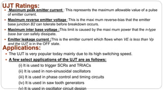
Downloaded 127 times


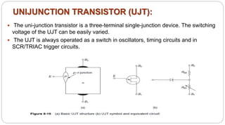
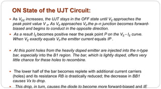
![OFF State of the UJT Circuit:
When a voltage VBB is applied across the two base terminals B1 and
B2, the potential of point p with respect to B1 is given by:
VP =[VBB/ (RB1 +RB2)]*RB1=η*RB1,
η is called the intrinsic stand off ratio with its typical value lying between
0.5 and 0.8.
The VEE source is applied to the emitter which is the p-side. Thus, the
emitter diode will be reverse-biased as long as VEE is less than Vx.
This is OFF state and is shown on the VE - IE curve as being a very
low current region.
In the OFF the UJT has a very high resistance between E and B1, and
IE is usually a negligible reverse leakage current. With no IE, the drop
across RE is zero and the emitter voltage equals the source voltage.](https://image.slidesharecdn.com/ec6202electronicdevicesandcircuitsunit2-170802050718/85/EC6202-ELECTRONIC-DEVICES-AND-CIRCUITS-Unit-2-116-320.jpg)


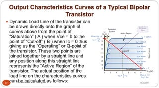
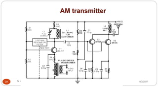
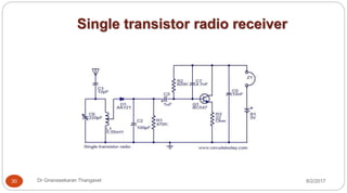
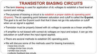
This document covers Unit 2 of a course on electronic devices and circuits, focusing on transistors including BJT, JFET, MOSFET, and others. It discusses their structures, operational characteristics, biasing, and configurations such as common base, common emitter, and common collector, along with practical examples and biasing methods. It aims to provide foundational knowledge on transistor operation in electronic applications.