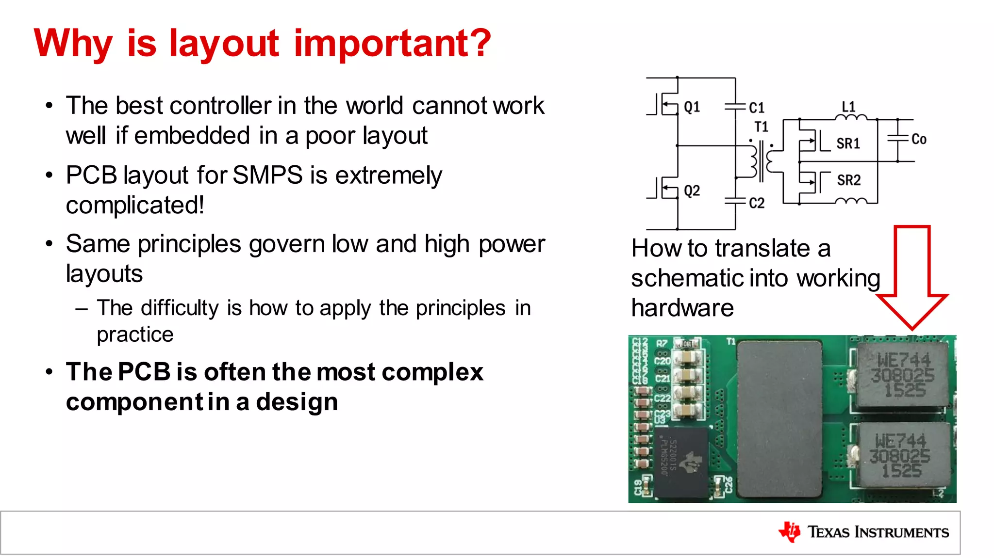
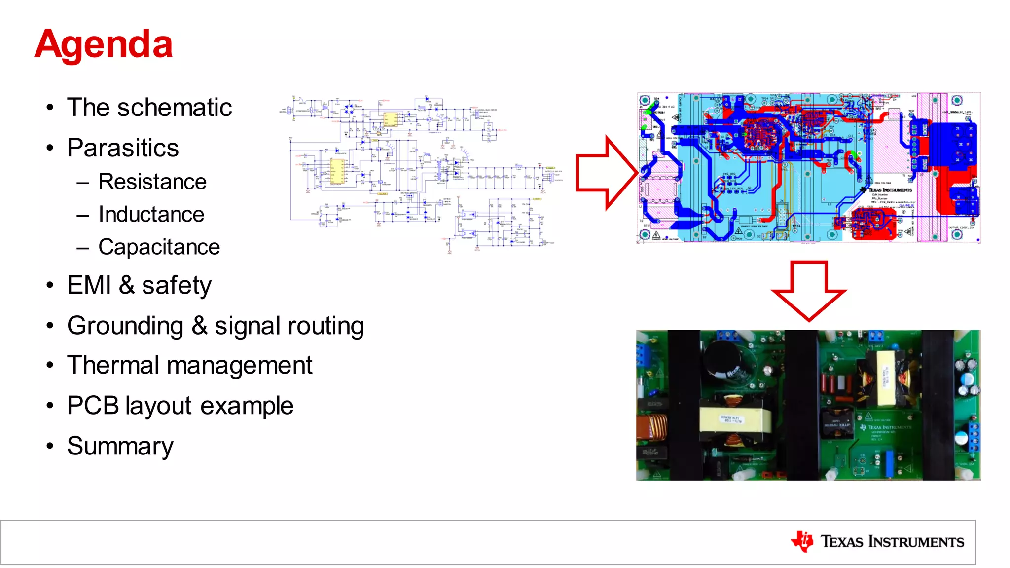
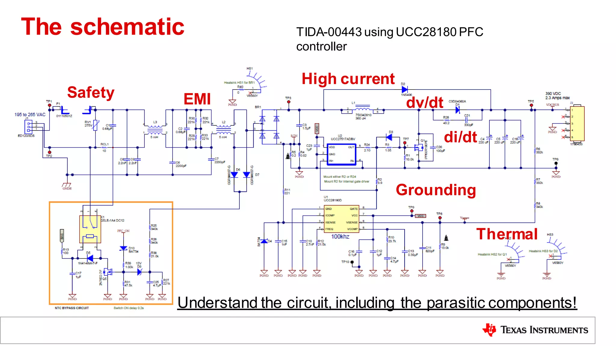
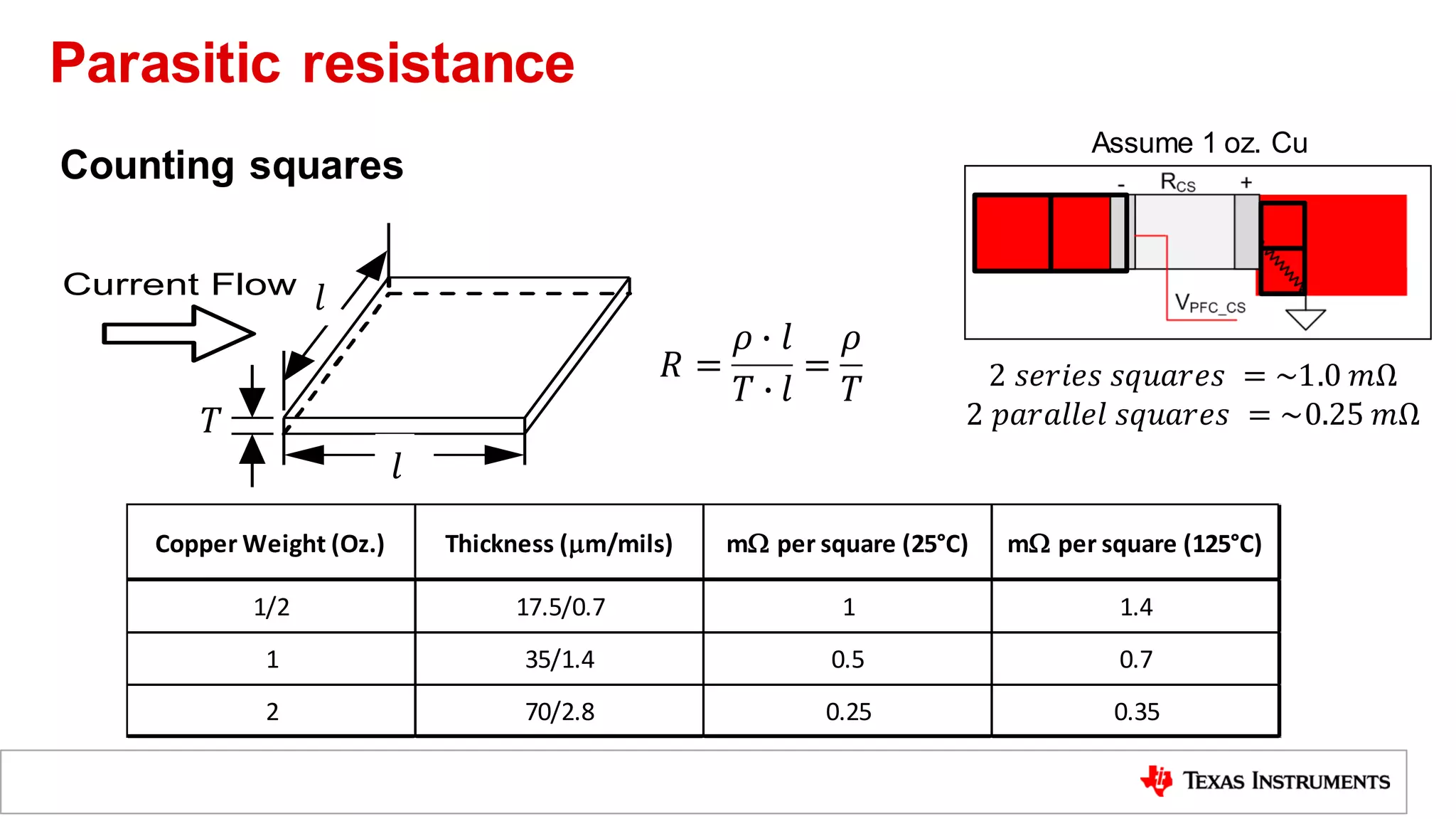
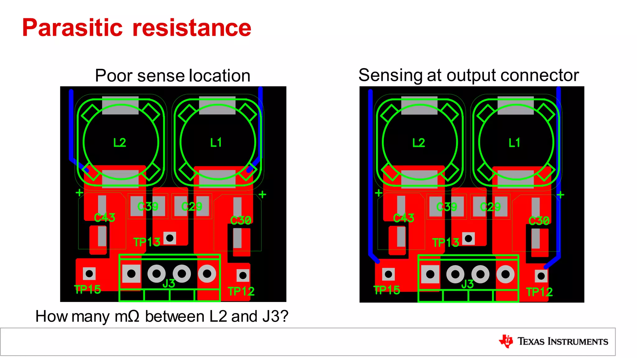
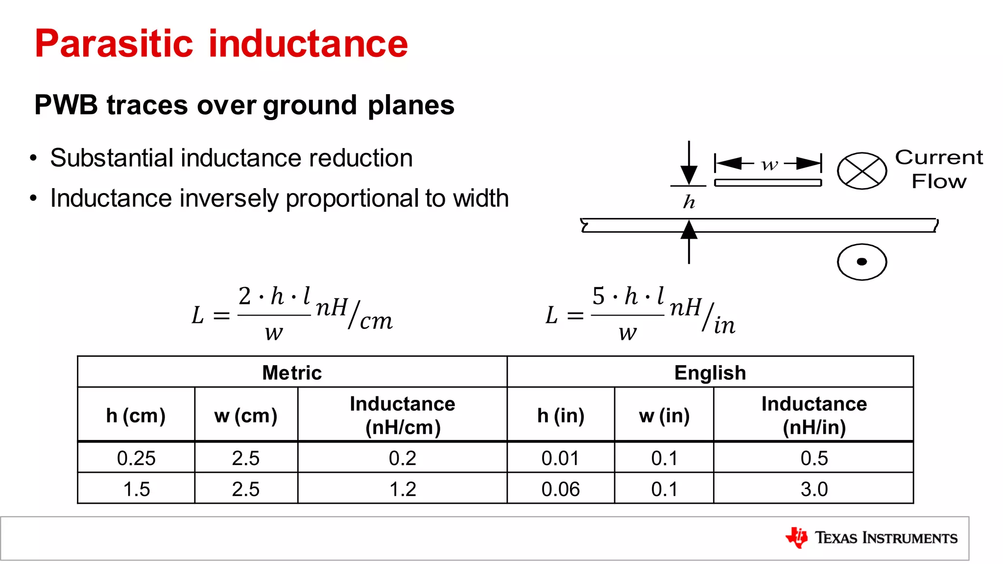
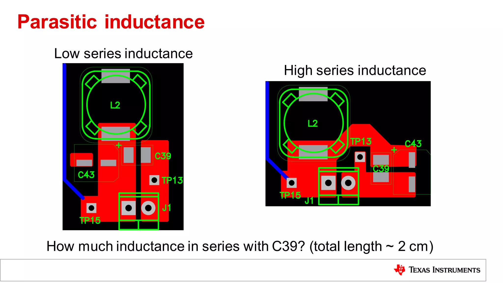
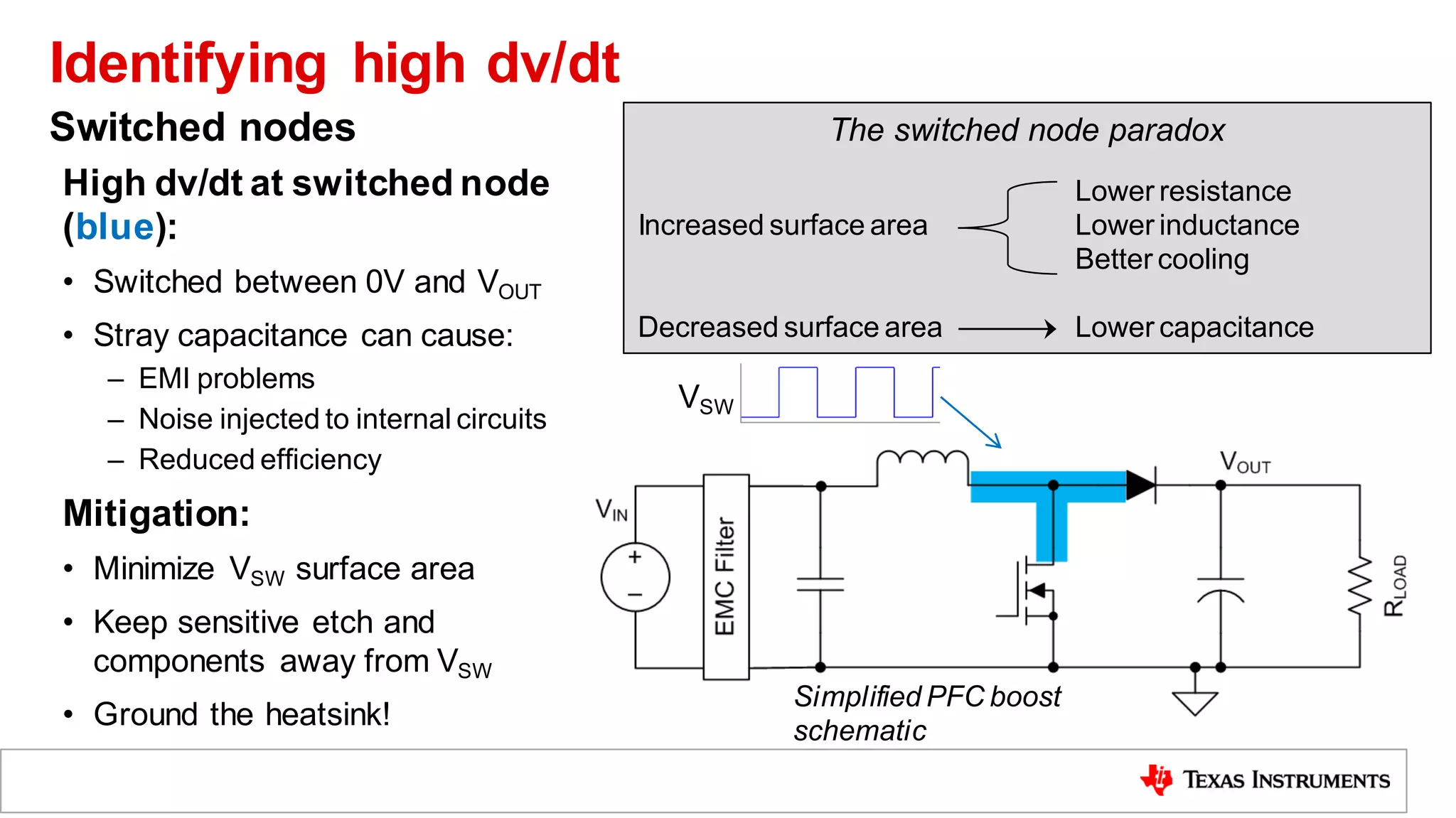
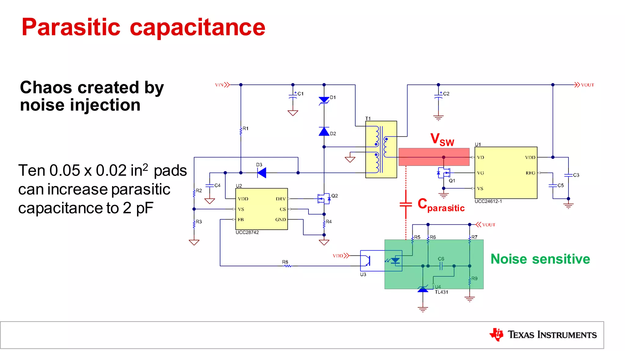
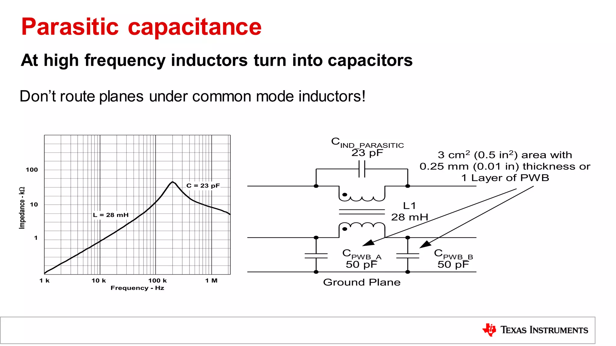
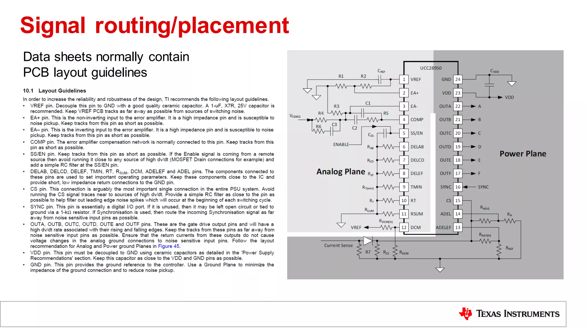
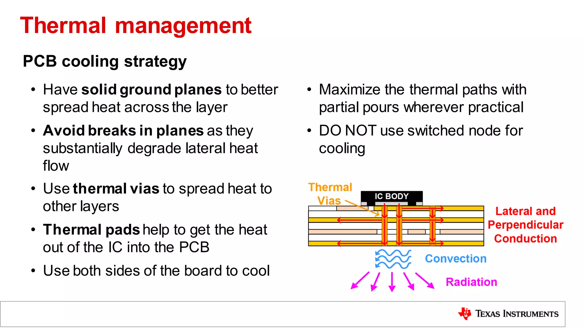
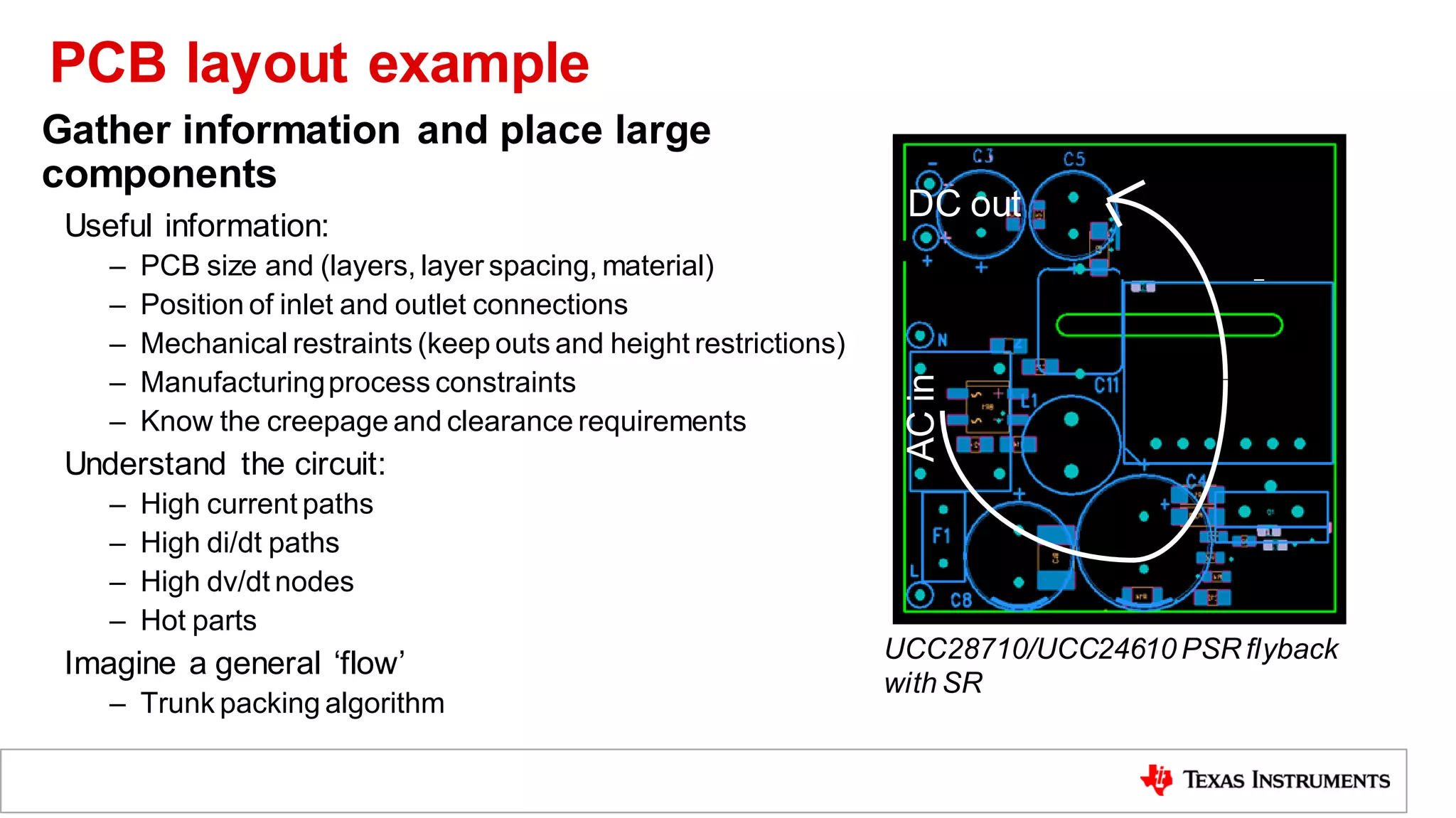
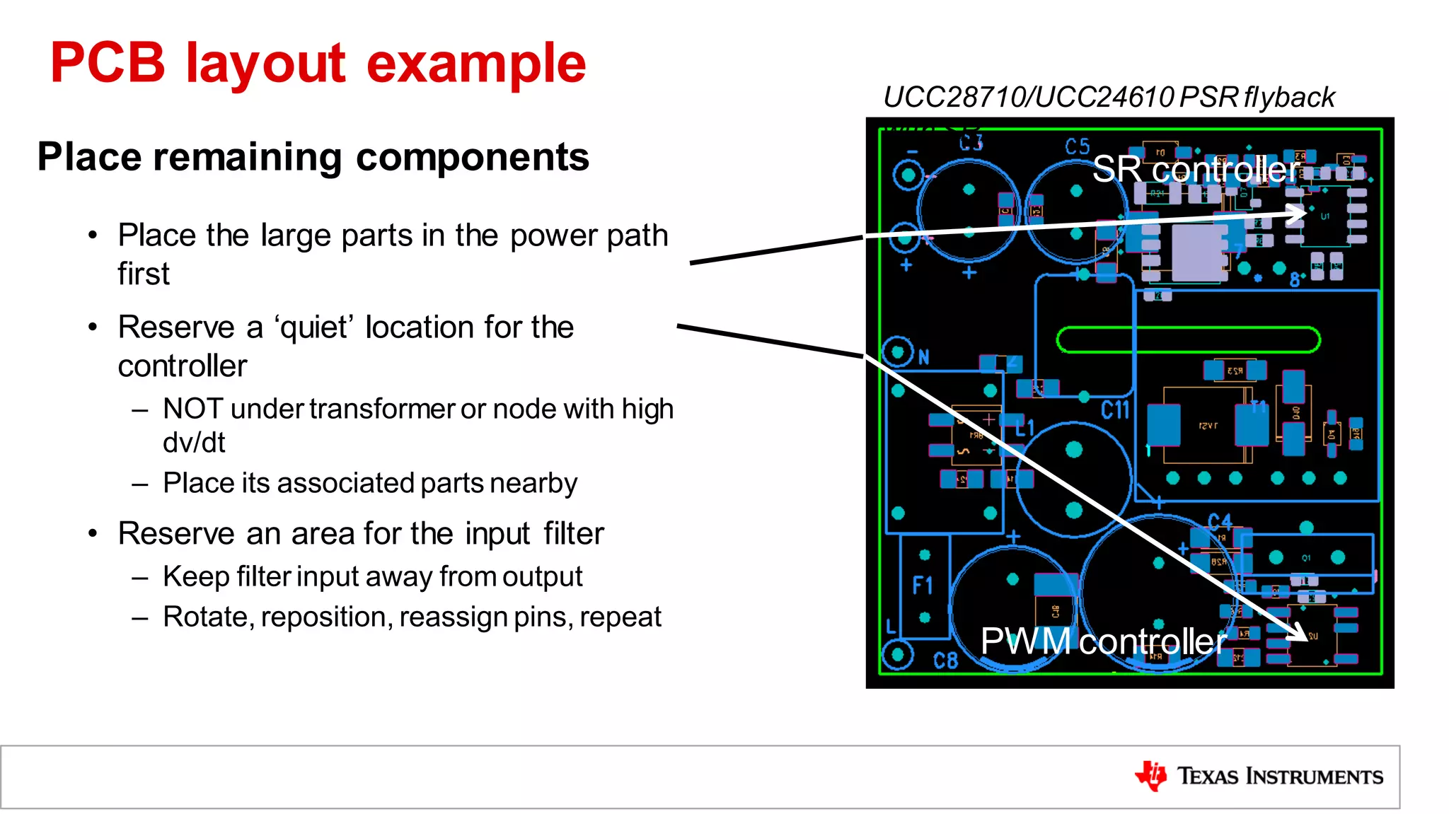
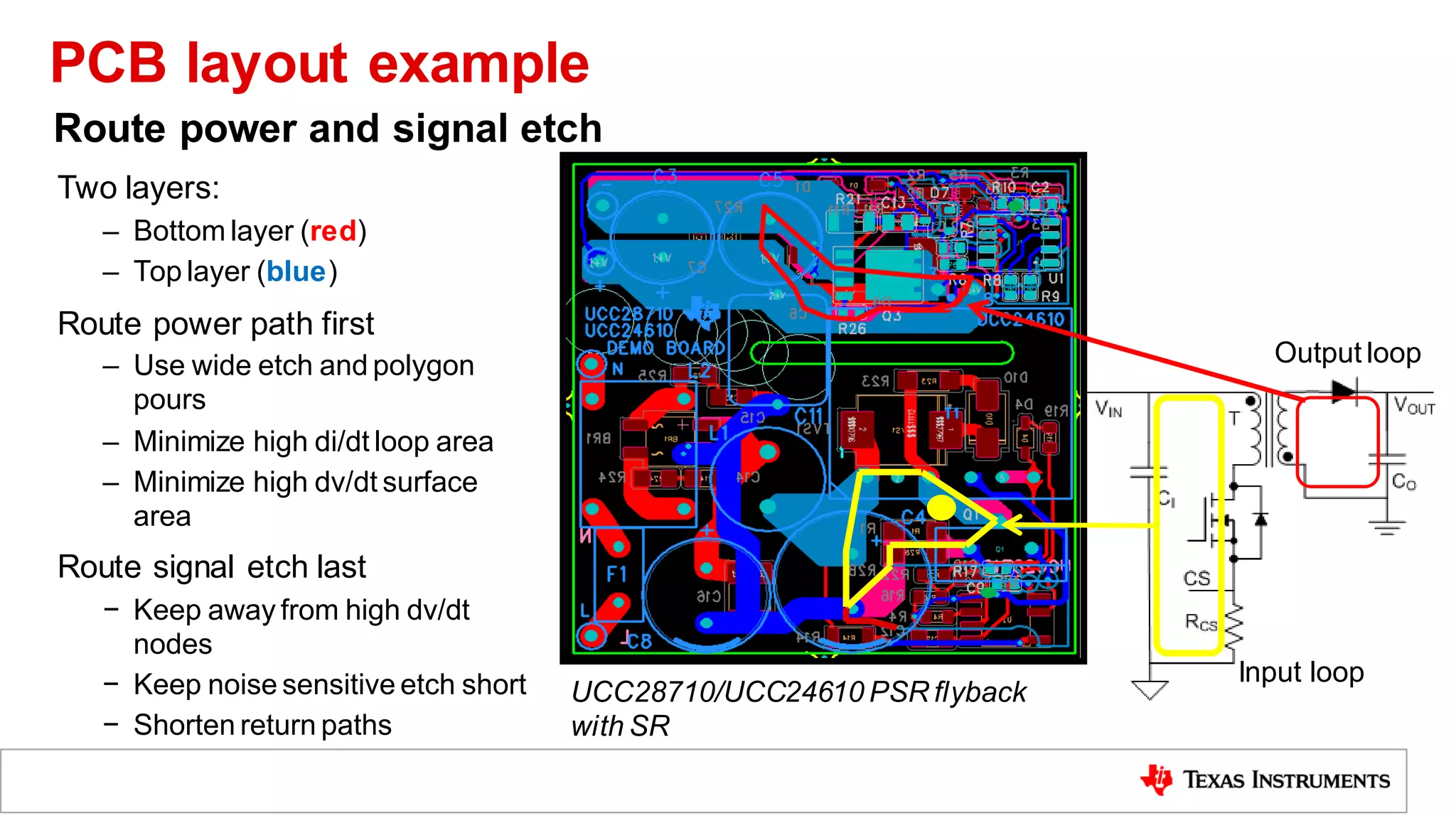
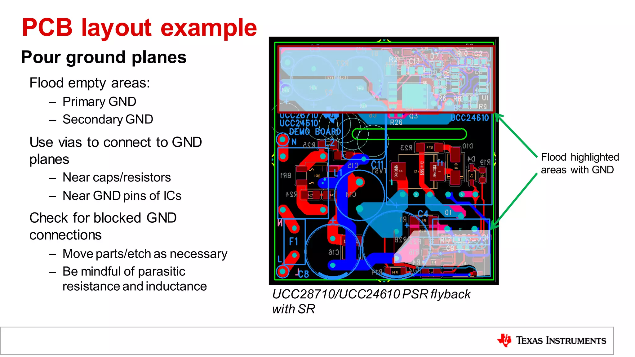
Printed circuit board layout for switched-
mode power supply
High Voltage Seminar 2021
Ben Genereaux
1
What will I get out of this session?
• The purpose of this session is to
introduce the concepts needed to
successfully layout a printed circuit
board (PCB) for a switched-mode
power supply (SMPS)
• This presentation is relevant to all
SMPS PCB layouts, from 1 W to 10 kW
• Part numbers mentioned:
– UCC28180
– UCC28742
– UCC28710
– UCC24612
– UCC24610
• Reference designs mentioned:
– TIDA-00443
Why is layout important?
• The best controller in the world cannot work
well if embedded in a poor layout
• PCB layout for SMPS is extremely
complicated!
• Same principles govern low and high power
layouts
– The difficulty is how to apply the principles in
practice
• The PCB is often the most complex
componentin a design
How to translate a
schematic into working
hardware
Agenda
• The schematic
• Parasitics
– Resistance
– Inductance
– Capacitance
• EMI & safety
• Grounding & signal routing
• Thermal management
• PCB layout example
• Summary
What are concerns for a power supply PCB
layout?
• Safety
• EMI
• Parasitic inductance
• Parasitic capacitance
• Parasitic resistance
• Thermal performance
• High dv/dt
• High di/dt
• Grounding
• Noise
EMI
di/dt
Safety
Thermal
dv/dt
High current
Grounding
Understand the circuit, including the parasitic components!
TIDA-00443 using UCC28180 PFC
controller
The schematic
Material mΩ-cm mΩ-in
Copper 1.70 0.67
Gold 2.2 0.87
Lead 22.0 8.66
Silver 1.5 0.59
Silver (plated) 1.8 0.71
Tin -lead 15 5.91
Tin (plated) 11 4.33
𝑅 =
𝜌 ∙ 𝑙
𝐴
𝜌 = 𝑟𝑒𝑠𝑖𝑠𝑡𝑖𝑣𝑖𝑡𝑦
ρ(Cu) = 0.67 mΩ-in at 25°C
Impacts?
• Regulation
• Efficiency
• Temperature rise
A
C
u
r
r
e
n
t
F
l
o
w

𝑙
You mean copper is not a perfect conductor?
𝑇𝐶𝑅𝐶𝑢 ≈ 4000 ൗ
𝑝𝑝𝑚
℃ +40% 𝑓𝑜𝑟 100℃ 𝑟𝑖𝑠𝑒
Parasitic resistance
𝑅 =
𝜌 ∙ 𝑙
𝑇 ∙ 𝑙
=
𝜌
𝑇 2 𝑠𝑒𝑟𝑖𝑒𝑠 𝑠𝑞𝑢𝑎𝑟𝑒𝑠 = ~1.0 𝑚Ω
2 𝑝𝑎𝑟𝑎𝑙𝑙𝑒𝑙 𝑠𝑞𝑢𝑎𝑟𝑒𝑠 = ~0.25 𝑚Ω
Assume 1 oz. Cu
Counting squares
t
Current Flow


𝑙
𝑙
𝑇
Copper Weight (Oz.) Thickness (m/mils) m per square (25°C) m per square (125°C)
1/2 17.5/0.7 1 1.4
1 35/1.4 0.5 0.7
2 70/2.8 0.25 0.35
Parasitic resistance
Typical rule of thumb is 1 A to 3 A per via
5 mm
(20 mils)
4.5 mm
(18 mils)
1.5 mm
(60 mils)
Current
Flow

A
𝑙
𝑅 =
𝜌 ∙ 𝑙
𝐴
𝑅 =
𝜌 ∙ 𝑙
𝜋 ∙ 𝑟𝑜
2 − 𝑟𝑖
2
𝑅 =
0.67 𝜇Ω∙ 𝑖𝑛 ∙ 0.06 𝑖𝑛
𝜋 ∙ 0.01 𝑖𝑛 2 − 0.009 𝑖𝑛 2 = 0.67 mΩ
Vias have resistance too
Parasitic resistance
How many mΩ between L2 and J3?
Sensing at output connector
Poor sense location
Parasitic resistance
Switched current loops
I/P loop (green)
• di/dt rates much lower
• Stray inductance is less critical
• CIN provides local low impedance
source
O/P loop (blue/red)
• Inductor current alternates between
MOSFET and diode paths
• Pulsating currents
• Stray inductance will cause voltage
spikes
Diode current
MOSFET
current
Inductor
current
I/P loop O/P loop
High di/dt
Low di/dt
Simplified PFC boost
schematic
Identifying high di/dt
Reverse recovery
Occurs when:
• MOSFET turns ON during CCM
operation (nearly every topology)
• Stray inductance will cause voltage
spikes
Mitigation:
• Minimize loop inductance
• Use low QRR rectifiers –
− SiC for high VOUT
− Schottky or ultra-fast diodes
− Sync rectifiers with low QRR
Simplified PFC boost
schematic
Identifying high di/dt
Gate drives
VGATE
IGATE
Simplified PFC boost
schematic
High di/dt in loop (yellow)
• Stray inductance:
– Limits drive current
– Can cause ringing
• Minimize loop inductance
High dv/dt on gate (blue)
• Can couple to noise-sensitive
nodes
• Minimize capacitance
Identifying high di/dt
Self inductance of PWB traces
• Due to the natural logarithmic relationship, large changes in conductor width have
minimal impact on inductance
W (mm/in) T(mm/in)
Inductance
(nH/cm or nH/in)
0.25/0.01 0.07/0.0028 10/24
2.5/0.1 0.07/0.0028 6/14
12.5/0.5 0.07/0.0028 2/6
w
t
C
u
r
r
e
n
t
F
l
o
w

𝑙
𝑇
𝐿 = 2 ∙ 𝑙 ∙ 𝑙𝑛
𝑙
𝑇 + 𝑊
+
1
2
ൗ
𝑛𝐻
𝑐𝑚
𝐿 = 5 ∙ 𝑙 ∙ 𝑙𝑛
𝑙
𝑇 + 𝑊
+
1
2
ൗ
𝑛𝐻
𝑖𝑛
Parasitic inductance
PWB traces over ground planes
• Substantial inductance reduction
• Inductance inversely proportional to width
Metric English
h (cm) w (cm)
Inductance
(nH/cm)
h (in) w (in)
Inductance
(nH/in)
0.25 2.5 0.2 0.01 0.1 0.5
1.5 2.5 1.2 0.06 0.1 3.0
w
h
Current
Flow
𝐿 =
2 ∙ ℎ ∙ 𝑙
𝑤
ൗ
𝑛𝐻
𝑐𝑚 𝐿 =
5 ∙ ℎ ∙ 𝑙
𝑤
ൗ
𝑛𝐻
𝑖𝑛
Parasitic inductance
Low series inductance
High series inductance
How much inductance in series with C39? (total length ~ 2 cm)
Parasitic inductance
Switched nodes
High dv/dt at switched node
(blue):
• Switched between 0V and VOUT
• Stray capacitance can cause:
– EMI problems
– Noise injected to internal circuits
– Reduced efficiency
Mitigation:
• Minimize VSW surface area
• Keep sensitive etch and
components away from VSW
• Ground the heatsink!
VSW
The switched node paradox
Lower resistance
Increased surface area Lower inductance
Better cooling
Decreased surface area Lower capacitance
Simplified PFC boost
schematic
Identifying high dv/dt
Sample capacitance calculation
Consider two 10 mil traces crossing with 10 mil PWB thickness
Not much capacitance but consider the area of all components connected to the feedback
network
Note: 10 mils = 0.00025 m
A = 0.00025 m x 0.00025 m
t
𝐶 =
𝜀𝑟 ∙ 𝜀0 ∙ 𝐴
𝑡
𝐶 =
5 ∙ 8.85× 10⁻¹² ൗ
𝐹
𝑚 ∙ 0.25 𝑚𝑚 2
2.5 𝑚𝑚
𝐶 = 0.01 𝑝𝐹
Parasitic capacitance
Chaos created by
noise injection
Ten 0.05 x 0.02 in2 pads
can increase parasitic
capacitance to 2 pF
VSW
Cparasitic
Noise sensitive
Parasitic capacitance
At high frequency inductors turn into capacitors
Don’t route planes under common mode inductors!
CIND_PARASITIC
23 pF
CPWB_A
50 pF
Ground Plane
CPWB_B
50 pF
L1
28 mH
3 cm2 (0.5 in2) area with
0.25 mm (0.01 in) thickness or
1 Layer of PWB
1 k
1
Impedance
-
k
Frequency - Hz
10
100
L = 28 mH
C = 23 pF
10 k 100 k 1 M
Parasitic capacitance
Magnetic coupling
• External fields couple between inductors
• Can cause EMI issues
• Consider alternate orientation of second
inductor to minimize coupling
• Use core shapes that provide better
shielding
EMI considerations
Input filter layout
• Place components away from noise
sources
• Common mode inductor T2 input pins
do not cross output pins
• No GND plane under EMI filter
• Wide, short etch used to minimize
losses
• Wide spacing between etches meets
high-voltage requirements and
minimizes coupling capacitance
EMI considerations
• Consult your safety expert!
• Create a very clear channel
between primary and secondary
• Spacing depends on:
– Type of insulation
– Pollution degree
– AC mains voltage
– Working voltage
• Types of insulation:
– Functional
– Basic/supplementary
– Reinforced
Separate hazardous voltages from user accessible points
Partial Clearance Dimensions (mm) from UL60950-1, Section 2.10.3,
Table 2H
Safety
Ground planes provide:
• Low resistance return paths
• Low inductance return paths
• Lateral heat spreading across board
General ground plane tips:
• Consider flooding empty areas with ground
• Avoid putting slots in GND planes
• Use jumpers on single layer boards to
improve GND planes
• Place as much GND under the IC as
possible
☺
Ground planes
Avoid coupling noise to sensitive nodes
• Maximize the separation
– Move the source, reduce Cstray
• Place capacitors and resistors near pins
• Place GND vias near caps, resistors,
and IC
• Minimize the unfiltered track length
Good
Bad
VSW VSW
Signal routing/placement
Data sheets normally contain
PCB layout guidelines
Signal routing/placement
• Have solid ground planes to better
spread heat across the layer
• Avoid breaks in planes as they
substantially degrade lateral heat
flow
• Use thermal vias to spread heat to
other layers
• Thermal padshelp to get the heat
out of the IC into the PCB
• Use both sides of the board to cool
• Maximize the thermal paths with
partial pours wherever practical
• DO NOT use switched node for
cooling
PCB cooling strategy
Thermal management
Why is Board A
hotter than Board
B?
• Traces on the bottom
layer prevent heat from
spreadingeffectively
• Removinghorizontal
trace for a more solid
bottom layer reduces IC
temp on board B
• Hottest component on B
is the catch diode
TOP
BOTTOM
BoardA Board B
Thermal management
Useful information:
– PCB size and (layers, layer spacing, material)
– Position of inlet and outlet connections
– Mechanical restraints (keep outs and height restrictions)
– Manufacturingprocess constraints
– Know the creepage and clearance requirements
Understand the circuit:
– High current paths
– High di/dt paths
– High dv/dt nodes
– Hot parts
Imagine a general ‘flow’
– Trunk packing algorithm
Gather information and place large
components
DC out
AC
in
UCC28710/UCC24610 PSR flyback
with SR
PCB layout example
• Place the large parts in the power path
first
• Reserve a ‘quiet’ location for the
controller
– NOT under transformer or node with high
dv/dt
– Place its associated parts nearby
• Reserve an area for the input filter
– Keep filter input away from output
– Rotate, reposition, reassign pins, repeat
PWM controller
SR controller
Place remaining components
UCC28710/UCC24610 PSR flyback
with SR
PCB layout example
Two layers:
– Bottom layer (red)
– Top layer (blue)
Route power path first
– Use wide etch and polygon
pours
– Minimize high di/dt loop area
– Minimize high dv/dt surface
area
Route signal etch last
− Keep away from high dv/dt
nodes
− Keep noise sensitive etch short
− Shorten return paths
Input loop
Output loop
Route power and signal etch
UCC28710/UCC24610 PSR flyback
with SR
PCB layout example
Flood empty areas:
– Primary GND
– Secondary GND
Use vias to connect to GND
planes
– Near caps/resistors
– Near GND pins of ICs
Check for blocked GND
connections
– Move parts/etch as necessary
– Be mindful of parasitic
resistance and inductance
Flood highlighted
areas with GND
Pour ground planes
UCC28710/UCC24610 PSR flyback
with SR
PCB layout example
• Understand your circuit: high current and di/dt paths, high dv/dt nodes
• Understand how parasitic resistance, inductance, and capacitance are manifested
• Understand how layout can significantly affect EMI
• Understand the safety requirements for your product
• Understand how heat is transferred through the PCB
• Follow a logical procedure:
– Place large parts, place small parts, power routing, signal routing, pour planes
• Have someone review your layout!
Summary: keys to a successful SMPS layout
• Constructing Your Power Supply - Layout Considerations; R. Kollman; 2004 TI
Power Supply Design Seminar; www.ti.com/seclit/ml/slup230/slup230.pdf
• Safety Considerations in Power Supply Design; B. Mammano and L. Bahra; 2004 TI
Power Supply Design Seminar; www.ti.com/seclit/ml/slup227/slup227.pdf
• Common Mistakes in DC/DC Converters and How to Fix Them; P. Shenoy and A.
Fagnani; 2018 TI Power Supply Design Seminar; www.ti.com/seclit/ml/slup384/slup384.pdf
• Grounding in Mixed-Signal Systems Demystified, Part 1 & Part 2; S. Pithadia and
S. More; 1Q 2013, TI Analog Applications Journal; www.ti.com/lit/an/slyt499/slyt499.pdf;
www.ti.com/lit/an/slyt512/slyt512.pdf
• Why Should You Count Squares; Brigitte; 2016 TI Power House Blog;
http://e2e.ti.com/blogs_/b/powerhouse/archive/2016/10/03/why-should-i-count-squares
Summary: references
Thank you
35
HVS content available for download at: www.ti.com/highvolt
©2021 Texas Instruments Incorporated.All rights reserved.
SLYP762
IMPORTANT NOTICE AND DISCLAIMER
TI PROVIDES TECHNICAL AND RELIABILITY DATA (INCLUDING DATASHEETS), DESIGN RESOURCES (INCLUDING REFERENCE
DESIGNS), APPLICATION OR OTHER DESIGN ADVICE, WEB TOOLS, SAFETY INFORMATION, AND OTHER RESOURCES “AS IS”
AND WITH ALL FAULTS, AND DISCLAIMS ALL WARRANTIES, EXPRESS AND IMPLIED, INCLUDING WITHOUT LIMITATION ANY
IMPLIED WARRANTIES OF MERCHANTABILITY, FITNESS FOR A PARTICULAR PURPOSE OR NON-INFRINGEMENT OF THIRD
PARTY INTELLECTUAL PROPERTY RIGHTS.
These resources are intended for skilled developers designing with TI products. You are solely responsible for (1) selecting the appropriate
TI products for your application, (2) designing, validating and testing your application, and (3) ensuring your application meets applicable
standards, and any other safety, security, or other requirements. These resources are subject to change without notice. TI grants you
permission to use these resources only for development of an application that uses the TI products described in the resource. Other
reproduction and display of these resources is prohibited. No license is granted to any other TI intellectual property right or to any third party
intellectual property right. TI disclaims responsibility for, and you will fully indemnify TI and its representatives against, any claims, damages,
costs, losses, and liabilities arising out of your use of these resources.
TI’s products are provided subject to TI’s Terms of Sale (https:www.ti.com/legal/termsofsale.html) or other applicable terms available either
on ti.com or provided in conjunction with such TI products. TI’s provision of these resources does not expand or otherwise alter TI’s
applicable warranties or warranty disclaimers for TI products.IMPORTANT NOTICE
Mailing Address: Texas Instruments, Post Office Box 655303, Dallas, Texas 75265
Copyright © 2021, Texas Instruments Incorporated

PCB Layout guidelines.pdf

  • 1.
    Printed circuit boardlayout for switched- mode power supply High Voltage Seminar 2021 Ben Genereaux 1
  • 2.
    What will Iget out of this session? • The purpose of this session is to introduce the concepts needed to successfully layout a printed circuit board (PCB) for a switched-mode power supply (SMPS) • This presentation is relevant to all SMPS PCB layouts, from 1 W to 10 kW • Part numbers mentioned: – UCC28180 – UCC28742 – UCC28710 – UCC24612 – UCC24610 • Reference designs mentioned: – TIDA-00443
  • 3.
    Why is layoutimportant? • The best controller in the world cannot work well if embedded in a poor layout • PCB layout for SMPS is extremely complicated! • Same principles govern low and high power layouts – The difficulty is how to apply the principles in practice • The PCB is often the most complex componentin a design How to translate a schematic into working hardware
  • 4.
    Agenda • The schematic •Parasitics – Resistance – Inductance – Capacitance • EMI & safety • Grounding & signal routing • Thermal management • PCB layout example • Summary
  • 5.
    What are concernsfor a power supply PCB layout? • Safety • EMI • Parasitic inductance • Parasitic capacitance • Parasitic resistance • Thermal performance • High dv/dt • High di/dt • Grounding • Noise
  • 6.
    EMI di/dt Safety Thermal dv/dt High current Grounding Understand thecircuit, including the parasitic components! TIDA-00443 using UCC28180 PFC controller The schematic
  • 7.
    Material mΩ-cm mΩ-in Copper1.70 0.67 Gold 2.2 0.87 Lead 22.0 8.66 Silver 1.5 0.59 Silver (plated) 1.8 0.71 Tin -lead 15 5.91 Tin (plated) 11 4.33 𝑅 = 𝜌 ∙ 𝑙 𝐴 𝜌 = 𝑟𝑒𝑠𝑖𝑠𝑡𝑖𝑣𝑖𝑡𝑦 ρ(Cu) = 0.67 mΩ-in at 25°C Impacts? • Regulation • Efficiency • Temperature rise A C u r r e n t F l o w  𝑙 You mean copper is not a perfect conductor? 𝑇𝐶𝑅𝐶𝑢 ≈ 4000 ൗ 𝑝𝑝𝑚 ℃ +40% 𝑓𝑜𝑟 100℃ 𝑟𝑖𝑠𝑒 Parasitic resistance
  • 8.
    𝑅 = 𝜌 ∙𝑙 𝑇 ∙ 𝑙 = 𝜌 𝑇 2 𝑠𝑒𝑟𝑖𝑒𝑠 𝑠𝑞𝑢𝑎𝑟𝑒𝑠 = ~1.0 𝑚Ω 2 𝑝𝑎𝑟𝑎𝑙𝑙𝑒𝑙 𝑠𝑞𝑢𝑎𝑟𝑒𝑠 = ~0.25 𝑚Ω Assume 1 oz. Cu Counting squares t Current Flow   𝑙 𝑙 𝑇 Copper Weight (Oz.) Thickness (m/mils) m per square (25°C) m per square (125°C) 1/2 17.5/0.7 1 1.4 1 35/1.4 0.5 0.7 2 70/2.8 0.25 0.35 Parasitic resistance
  • 9.
    Typical rule ofthumb is 1 A to 3 A per via 5 mm (20 mils) 4.5 mm (18 mils) 1.5 mm (60 mils) Current Flow  A 𝑙 𝑅 = 𝜌 ∙ 𝑙 𝐴 𝑅 = 𝜌 ∙ 𝑙 𝜋 ∙ 𝑟𝑜 2 − 𝑟𝑖 2 𝑅 = 0.67 𝜇Ω∙ 𝑖𝑛 ∙ 0.06 𝑖𝑛 𝜋 ∙ 0.01 𝑖𝑛 2 − 0.009 𝑖𝑛 2 = 0.67 mΩ Vias have resistance too Parasitic resistance
  • 10.
    How many mΩbetween L2 and J3? Sensing at output connector Poor sense location Parasitic resistance
  • 11.
    Switched current loops I/Ploop (green) • di/dt rates much lower • Stray inductance is less critical • CIN provides local low impedance source O/P loop (blue/red) • Inductor current alternates between MOSFET and diode paths • Pulsating currents • Stray inductance will cause voltage spikes Diode current MOSFET current Inductor current I/P loop O/P loop High di/dt Low di/dt Simplified PFC boost schematic Identifying high di/dt
  • 12.
    Reverse recovery Occurs when: •MOSFET turns ON during CCM operation (nearly every topology) • Stray inductance will cause voltage spikes Mitigation: • Minimize loop inductance • Use low QRR rectifiers – − SiC for high VOUT − Schottky or ultra-fast diodes − Sync rectifiers with low QRR Simplified PFC boost schematic Identifying high di/dt
  • 13.
    Gate drives VGATE IGATE Simplified PFCboost schematic High di/dt in loop (yellow) • Stray inductance: – Limits drive current – Can cause ringing • Minimize loop inductance High dv/dt on gate (blue) • Can couple to noise-sensitive nodes • Minimize capacitance Identifying high di/dt
  • 14.
    Self inductance ofPWB traces • Due to the natural logarithmic relationship, large changes in conductor width have minimal impact on inductance W (mm/in) T(mm/in) Inductance (nH/cm or nH/in) 0.25/0.01 0.07/0.0028 10/24 2.5/0.1 0.07/0.0028 6/14 12.5/0.5 0.07/0.0028 2/6 w t C u r r e n t F l o w  𝑙 𝑇 𝐿 = 2 ∙ 𝑙 ∙ 𝑙𝑛 𝑙 𝑇 + 𝑊 + 1 2 ൗ 𝑛𝐻 𝑐𝑚 𝐿 = 5 ∙ 𝑙 ∙ 𝑙𝑛 𝑙 𝑇 + 𝑊 + 1 2 ൗ 𝑛𝐻 𝑖𝑛 Parasitic inductance
  • 15.
    PWB traces overground planes • Substantial inductance reduction • Inductance inversely proportional to width Metric English h (cm) w (cm) Inductance (nH/cm) h (in) w (in) Inductance (nH/in) 0.25 2.5 0.2 0.01 0.1 0.5 1.5 2.5 1.2 0.06 0.1 3.0 w h Current Flow 𝐿 = 2 ∙ ℎ ∙ 𝑙 𝑤 ൗ 𝑛𝐻 𝑐𝑚 𝐿 = 5 ∙ ℎ ∙ 𝑙 𝑤 ൗ 𝑛𝐻 𝑖𝑛 Parasitic inductance
  • 16.
    Low series inductance Highseries inductance How much inductance in series with C39? (total length ~ 2 cm) Parasitic inductance
  • 17.
    Switched nodes High dv/dtat switched node (blue): • Switched between 0V and VOUT • Stray capacitance can cause: – EMI problems – Noise injected to internal circuits – Reduced efficiency Mitigation: • Minimize VSW surface area • Keep sensitive etch and components away from VSW • Ground the heatsink! VSW The switched node paradox Lower resistance Increased surface area Lower inductance Better cooling Decreased surface area Lower capacitance Simplified PFC boost schematic Identifying high dv/dt
  • 18.
    Sample capacitance calculation Considertwo 10 mil traces crossing with 10 mil PWB thickness Not much capacitance but consider the area of all components connected to the feedback network Note: 10 mils = 0.00025 m A = 0.00025 m x 0.00025 m t 𝐶 = 𝜀𝑟 ∙ 𝜀0 ∙ 𝐴 𝑡 𝐶 = 5 ∙ 8.85× 10⁻¹² ൗ 𝐹 𝑚 ∙ 0.25 𝑚𝑚 2 2.5 𝑚𝑚 𝐶 = 0.01 𝑝𝐹 Parasitic capacitance
  • 19.
    Chaos created by noiseinjection Ten 0.05 x 0.02 in2 pads can increase parasitic capacitance to 2 pF VSW Cparasitic Noise sensitive Parasitic capacitance
  • 20.
    At high frequencyinductors turn into capacitors Don’t route planes under common mode inductors! CIND_PARASITIC 23 pF CPWB_A 50 pF Ground Plane CPWB_B 50 pF L1 28 mH 3 cm2 (0.5 in2) area with 0.25 mm (0.01 in) thickness or 1 Layer of PWB 1 k 1 Impedance - k Frequency - Hz 10 100 L = 28 mH C = 23 pF 10 k 100 k 1 M Parasitic capacitance
  • 21.
    Magnetic coupling • Externalfields couple between inductors • Can cause EMI issues • Consider alternate orientation of second inductor to minimize coupling • Use core shapes that provide better shielding EMI considerations
  • 22.
    Input filter layout •Place components away from noise sources • Common mode inductor T2 input pins do not cross output pins • No GND plane under EMI filter • Wide, short etch used to minimize losses • Wide spacing between etches meets high-voltage requirements and minimizes coupling capacitance EMI considerations
  • 23.
    • Consult yoursafety expert! • Create a very clear channel between primary and secondary • Spacing depends on: – Type of insulation – Pollution degree – AC mains voltage – Working voltage • Types of insulation: – Functional – Basic/supplementary – Reinforced Separate hazardous voltages from user accessible points Partial Clearance Dimensions (mm) from UL60950-1, Section 2.10.3, Table 2H Safety
  • 24.
    Ground planes provide: •Low resistance return paths • Low inductance return paths • Lateral heat spreading across board General ground plane tips: • Consider flooding empty areas with ground • Avoid putting slots in GND planes • Use jumpers on single layer boards to improve GND planes • Place as much GND under the IC as possible ☺ Ground planes
  • 25.
    Avoid coupling noiseto sensitive nodes • Maximize the separation – Move the source, reduce Cstray • Place capacitors and resistors near pins • Place GND vias near caps, resistors, and IC • Minimize the unfiltered track length Good Bad VSW VSW Signal routing/placement
  • 26.
    Data sheets normallycontain PCB layout guidelines Signal routing/placement
  • 27.
    • Have solidground planes to better spread heat across the layer • Avoid breaks in planes as they substantially degrade lateral heat flow • Use thermal vias to spread heat to other layers • Thermal padshelp to get the heat out of the IC into the PCB • Use both sides of the board to cool • Maximize the thermal paths with partial pours wherever practical • DO NOT use switched node for cooling PCB cooling strategy Thermal management
  • 28.
    Why is BoardA hotter than Board B? • Traces on the bottom layer prevent heat from spreadingeffectively • Removinghorizontal trace for a more solid bottom layer reduces IC temp on board B • Hottest component on B is the catch diode TOP BOTTOM BoardA Board B Thermal management
  • 29.
    Useful information: – PCBsize and (layers, layer spacing, material) – Position of inlet and outlet connections – Mechanical restraints (keep outs and height restrictions) – Manufacturingprocess constraints – Know the creepage and clearance requirements Understand the circuit: – High current paths – High di/dt paths – High dv/dt nodes – Hot parts Imagine a general ‘flow’ – Trunk packing algorithm Gather information and place large components DC out AC in UCC28710/UCC24610 PSR flyback with SR PCB layout example
  • 30.
    • Place thelarge parts in the power path first • Reserve a ‘quiet’ location for the controller – NOT under transformer or node with high dv/dt – Place its associated parts nearby • Reserve an area for the input filter – Keep filter input away from output – Rotate, reposition, reassign pins, repeat PWM controller SR controller Place remaining components UCC28710/UCC24610 PSR flyback with SR PCB layout example
  • 31.
    Two layers: – Bottomlayer (red) – Top layer (blue) Route power path first – Use wide etch and polygon pours – Minimize high di/dt loop area – Minimize high dv/dt surface area Route signal etch last − Keep away from high dv/dt nodes − Keep noise sensitive etch short − Shorten return paths Input loop Output loop Route power and signal etch UCC28710/UCC24610 PSR flyback with SR PCB layout example
  • 32.
    Flood empty areas: –Primary GND – Secondary GND Use vias to connect to GND planes – Near caps/resistors – Near GND pins of ICs Check for blocked GND connections – Move parts/etch as necessary – Be mindful of parasitic resistance and inductance Flood highlighted areas with GND Pour ground planes UCC28710/UCC24610 PSR flyback with SR PCB layout example
  • 33.
    • Understand yourcircuit: high current and di/dt paths, high dv/dt nodes • Understand how parasitic resistance, inductance, and capacitance are manifested • Understand how layout can significantly affect EMI • Understand the safety requirements for your product • Understand how heat is transferred through the PCB • Follow a logical procedure: – Place large parts, place small parts, power routing, signal routing, pour planes • Have someone review your layout! Summary: keys to a successful SMPS layout
  • 34.
    • Constructing YourPower Supply - Layout Considerations; R. Kollman; 2004 TI Power Supply Design Seminar; www.ti.com/seclit/ml/slup230/slup230.pdf • Safety Considerations in Power Supply Design; B. Mammano and L. Bahra; 2004 TI Power Supply Design Seminar; www.ti.com/seclit/ml/slup227/slup227.pdf • Common Mistakes in DC/DC Converters and How to Fix Them; P. Shenoy and A. Fagnani; 2018 TI Power Supply Design Seminar; www.ti.com/seclit/ml/slup384/slup384.pdf • Grounding in Mixed-Signal Systems Demystified, Part 1 & Part 2; S. Pithadia and S. More; 1Q 2013, TI Analog Applications Journal; www.ti.com/lit/an/slyt499/slyt499.pdf; www.ti.com/lit/an/slyt512/slyt512.pdf • Why Should You Count Squares; Brigitte; 2016 TI Power House Blog; http://e2e.ti.com/blogs_/b/powerhouse/archive/2016/10/03/why-should-i-count-squares Summary: references
  • 35.
    Thank you 35 HVS contentavailable for download at: www.ti.com/highvolt
  • 36.
    ©2021 Texas InstrumentsIncorporated.All rights reserved. SLYP762
  • 37.
    IMPORTANT NOTICE ANDDISCLAIMER TI PROVIDES TECHNICAL AND RELIABILITY DATA (INCLUDING DATASHEETS), DESIGN RESOURCES (INCLUDING REFERENCE DESIGNS), APPLICATION OR OTHER DESIGN ADVICE, WEB TOOLS, SAFETY INFORMATION, AND OTHER RESOURCES “AS IS” AND WITH ALL FAULTS, AND DISCLAIMS ALL WARRANTIES, EXPRESS AND IMPLIED, INCLUDING WITHOUT LIMITATION ANY IMPLIED WARRANTIES OF MERCHANTABILITY, FITNESS FOR A PARTICULAR PURPOSE OR NON-INFRINGEMENT OF THIRD PARTY INTELLECTUAL PROPERTY RIGHTS. These resources are intended for skilled developers designing with TI products. You are solely responsible for (1) selecting the appropriate TI products for your application, (2) designing, validating and testing your application, and (3) ensuring your application meets applicable standards, and any other safety, security, or other requirements. These resources are subject to change without notice. TI grants you permission to use these resources only for development of an application that uses the TI products described in the resource. Other reproduction and display of these resources is prohibited. No license is granted to any other TI intellectual property right or to any third party intellectual property right. TI disclaims responsibility for, and you will fully indemnify TI and its representatives against, any claims, damages, costs, losses, and liabilities arising out of your use of these resources. TI’s products are provided subject to TI’s Terms of Sale (https:www.ti.com/legal/termsofsale.html) or other applicable terms available either on ti.com or provided in conjunction with such TI products. TI’s provision of these resources does not expand or otherwise alter TI’s applicable warranties or warranty disclaimers for TI products.IMPORTANT NOTICE Mailing Address: Texas Instruments, Post Office Box 655303, Dallas, Texas 75265 Copyright © 2021, Texas Instruments Incorporated