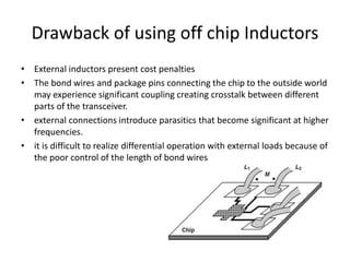
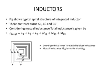
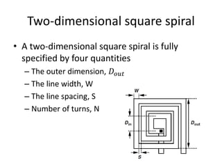
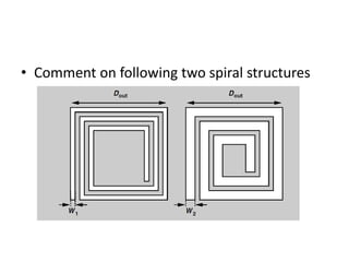
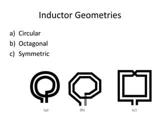
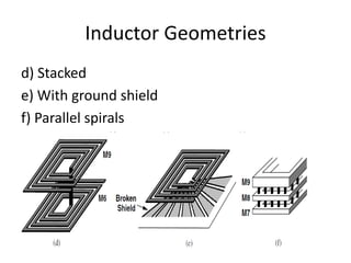
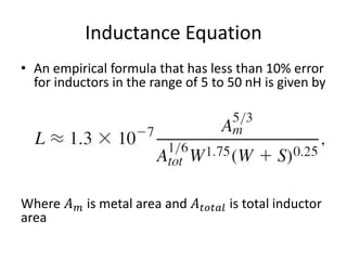
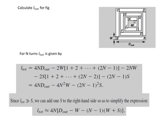
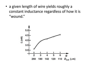
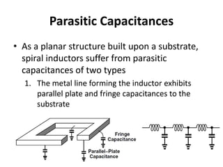
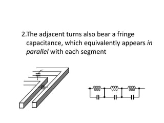
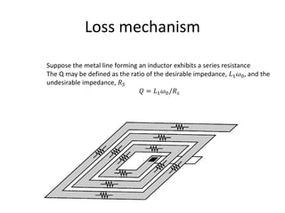
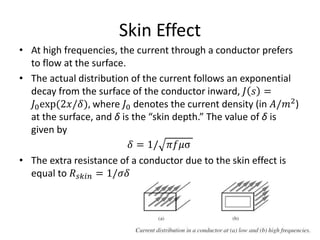
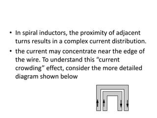
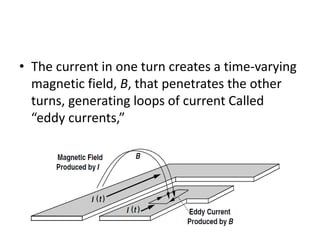
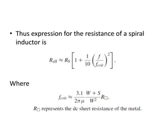
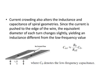
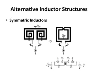
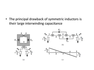
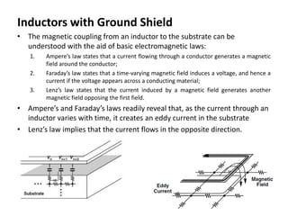
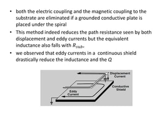
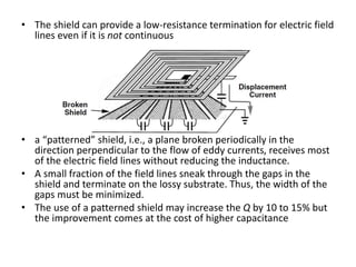
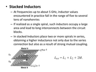
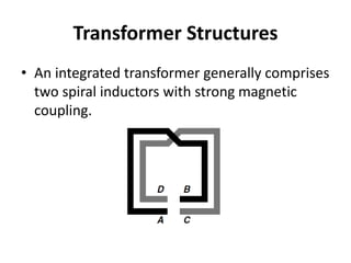
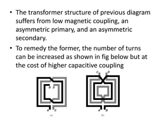
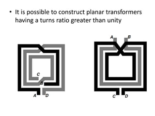
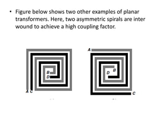
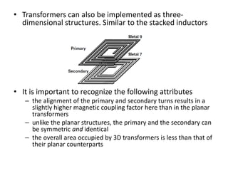
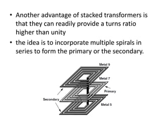
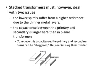
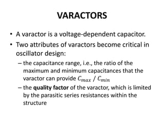
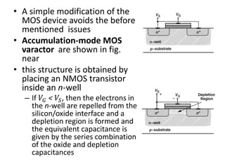
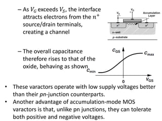
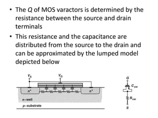
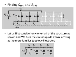
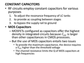
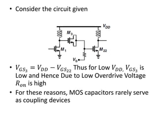
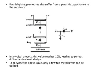
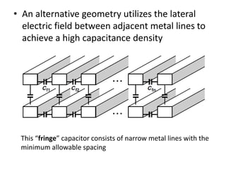
This document discusses the fabrication of passive devices in integrated circuits, including inductors, transformers, and varactors. It notes the need for on-chip inductors and transformers to avoid issues with off-chip components. Common structures for on-chip inductors include spiral geometries, which can be circular, octagonal, or stacked. Methods to reduce parasitic capacitances in inductors include using ground shields or increasing line spacing. Transformers are typically built from coupled spiral inductors and can be planar or stacked. Varactors are voltage-dependent capacitors important for oscillator design with a critical capacitance range.

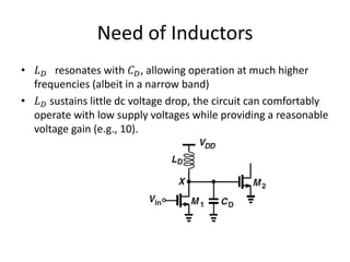
![Need of Inductors
• Modern RF design needs many inductors
• This topology suffers from two serious drawbacks
• the bandwidth at node X is limited to 1/[(𝑅 𝐷| 𝑟𝑂1
𝐶 𝐷 ]
• the voltage headroom trades with the voltage gain, g 𝑚1
(𝑅 𝐷| 𝑟𝑂1
• CMOS technology scaling tends to improve the former but at the cost of the latter
• For example, in 65-nm technology with a 1-V supply, the circuit provides a
bandwidth of several gigahertz but a voltage gain in the range of 3 to 4.](https://image.slidesharecdn.com/passivedevicefabricationinic-181114110016/85/Passive-device-fabrication-in-Integrated-circuits-3-320.jpg)