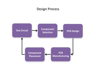
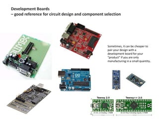
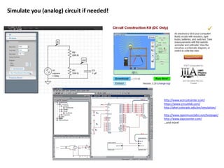
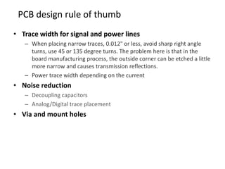
This document provides an overview of the electronic circuit design and component selection process. It discusses testing circuits, selecting components, PCB design, manufacturing, and assembly. Key steps include testing circuits using breadboards or simulations, choosing components based on specifications, laying out PCB traces with consideration for power/ground planes and signal routing, and assembling boards using soldering or pick-and-place machines. Tips are provided for design rules, decoupling, and ordering PCB fabrication and assembly services.


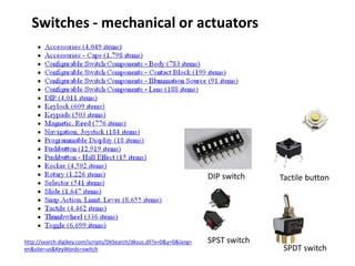
![Switches
Electronics
specification
Expansion Description Symbol
SPST Single pole, single throw
A simple on-off switch: The two terminals are either
connected together or disconnected from each other.
An example is a light switch.
SPDT Single pole, double throw
A simple changeover switch: C (COM, Common) is
connected to L1 or to L2.
SPCO
SPTT, c.o.
Single pole changeover
or
Single pole, centre off or
Single Pole, Triple Throw
Similar to SPDT. Some suppliers use SPCO/SPTT for
switches with a stable off position in the centre
and SPDT for those without.[citation needed]
DPST Double pole, single throw
Equivalent to two SPST switches controlled by a single
mechanism
DPDT Double pole, double throw
Equivalent to two SPDT switches controlled by a single
mechanism.
DPCO
Double pole changeover
or Double pole, centre off
Equivalent to DPDT. Some suppliers use DPCO for
switches with a stable off position in the centre
and DPDT for those without.
http://en.wikipedia.org/wiki/Switch](https://image.slidesharecdn.com/electroniccircuitdesignandcomponentselection-240215045723-af6e4da8/85/Electronic-circuit-design-and-component-selection-pptx-14-320.jpg)


![http://circuitcalculator.com/wordpress/2006/01/31/pcb-trace-width-calculator/
Area[mils^2] = (I[Amps]/(k*(Temp_Rise[deg. C])^b))^(1/c)
Then, the Width is calculated:
Width[mils] = Area[mils^2]/(Thickness[oz]*1.378[mils/oz])
Trace width calculation – to avoid voltage drop
(trace resistance) and over heating](https://image.slidesharecdn.com/electroniccircuitdesignandcomponentselection-240215045723-af6e4da8/85/Electronic-circuit-design-and-component-selection-pptx-26-320.jpg)


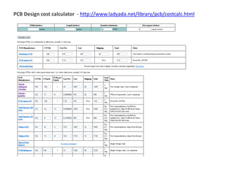


![How to order PCB assembly
• You can ask them to order the parts or you can send them the parts.
• Files needed -
– Bill of Materials(BOM)
– Centroid data
• Centroid data (aka Insertion or Pick-and-place or XY data) - This is the machine file, which should
include: X, Y, Theta, Side of Board (Top or Bottom), and Reference Designator.
• The BOM from Eagle is not the format that they like.
For generating Centroid data, see
http://www.screamingcircuits.com/services/how-it-works.aspx#eagle
Footprint Comment LibRef Designator Description Quantity Distributor Distributor part ID
1608[0603] 100nF Cap Semi
C11, C14, C17, C20,
C34, C35, C51, C62,
C63
Capacitor 9 Digi-key 490-1524-6-ND](https://image.slidesharecdn.com/electroniccircuitdesignandcomponentselection-240215045723-af6e4da8/85/Electronic-circuit-design-and-component-selection-pptx-43-320.jpg)