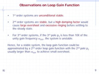
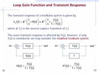
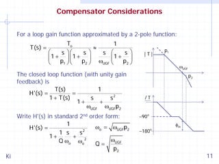
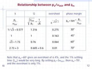
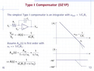
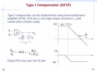
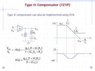
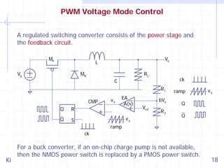
This document discusses stability and compensation techniques for switching converters. It begins by introducing feedback systems and stability criteria such as the Nyquist criterion and Bode plots. It then examines loop gain functions of different orders and their impact on stability and transient response. Several common compensation techniques are described, including type I, II, and III compensators. The document concludes by discussing stability evaluation based on line and load transients and current mode pulse width modulation with compensation ramps.


![Type II Compensator (1Z2P)
Type II compensator consists of a pole-zero pair with ωz<ωp, and a
maximum phase boosting of 90o is possible.
R2
|A|
C2
1
C2R 2
C1
ωUGF =
1 / C1R1
R1
Vin
Vref
Vout
Vout
1 + sC2R 2
=−
Vin
s(C1 + C 2 )R1 [1 + s(C1 || C 2 )R 2 ]
A(s) ≈
Ki
(1 + sC2R 2 )
sC2R1 (1 + sC1R 2 )
1
C1R 2
(C1 << C2 )
1 / C2R1
ω
/A
ω
90 o phase
boosting
−90 o
15](https://image.slidesharecdn.com/tu0403switcherki2009isic-140305063913-phpapp02/85/IC-Design-of-Power-Management-Circuits-III-15-320.jpg)
![Type III Compensator (2Z3P)
Type III compensator consists of two pole-zero pairs, and phase
boosting of 180o is possible to compensate for complex poles.
R2
R3
Vin
C3
R1
Vref
|A|
C2
1
C2R 2
C1
Vout
1
C2R1
/A
Vout
(1 + sC 2R 2 )[1 + sC3 (R1 + R 3 )]
=−
+90 o
Vin
s(C1 + C2 )R1 (1 + sC1 || C2R 2 )(1 + sC3R 3 )
(1 + sC2R 2 )(1 + sC 3R1 )
A(s) ≈
sC2R1 (1 + sC1R 2 )(1 + sC 3R 3 )
Ki
(C1 <<C2 , R1>>R 3 )
1
C3R1
1
1
C1R 2 C3R 3
ωUGF
1
=
C1R 3
180o
boosting
ω
ω
−90 o
17](https://image.slidesharecdn.com/tu0403switcherki2009isic-140305063913-phpapp02/85/IC-Design-of-Power-Management-Circuits-III-17-320.jpg)
![Loop Gains of Voltage Mode CCM Converters
The system loop gain is T(s) = A(s)×H(s), where A(s) is the frequency
response of the EA (compensator). Loop gains of voltage mode PWM
CCM converters with trailing-edge modulation are compiled. Parasitic
resistances except ESR are excluded [Ki 98].
Buck:
Boost:
T(s) = A(s) ×
bVo 1 + sCR esr
.
sL
DVm
+ s 2LC
1+
RL
bVo [1 − sL / (D '2 R L )]
T(s) = A(s) ×
.
D ' Vm
sL
s 2LC
+
1+ 2
D ' R L D '2
b | Vo | [1 − sDL / (D '2 R L )]
.
Buck-boost: T(s) = A(s) ×
DD ' Vm
sL
s 2LC
+
1+ 2
D ' R L D '2
Ki
19](https://image.slidesharecdn.com/tu0403switcherki2009isic-140305063913-phpapp02/85/IC-Design-of-Power-Management-Circuits-III-19-320.jpg)
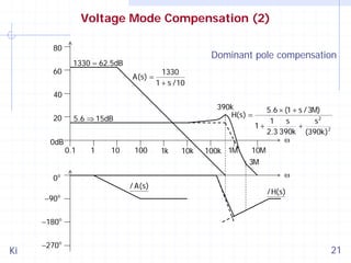
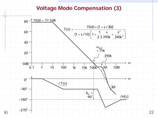
![Voltage Mode Compensation (1)
Example: Consider a buck converter with the following parameters:
Vdd=4.2V, Vo=1.8V (D=0.429), Vm=0.5V, b=0.667
L=2μH, C=3.3μF, RL=1.8Ω (Io=1A), Resr=100mΩ, fs=1MHz
The system loop gain is given by
T(s) = A(s) ⋅
5.6 × [1 + s /(3M)]
A(s) × 5.6 × [1 + s /(3M)]
=
1
s
s2
1 s
s2
+
+ 2
1+
1+
2
2.3 390k (390k)
Q ωo ωo
The system loop gain consists of a pair of complex poles, and one
strategy is to use dominant pole compensation.
For a buck converter, the complex pole frequency ωo/2π is 10 to 30
times lower than the switching frequency fs.
Ki
20](https://image.slidesharecdn.com/tu0403switcherki2009isic-140305063913-phpapp02/85/IC-Design-of-Power-Management-Circuits-III-20-320.jpg)
![Loop Gain of Current Mode Buck Converter (1)
The loop gain of a current-mode CCM buck converter with trailingedge modulation is shown below. Others can be found in [Ki 98].
Buck:
1
1
(1 + sCR esr )
CR f n1D ' T
T(s) = A(s) ×
⎛ 1
1 ⎞
1 1 ⎛ 1 (n1D '− D)T ⎞
2
+
+
+
s + s⎜
⎟
CR L n1D ' T ⎟ n1D ' T C ⎜ R L
L
⎝
⎠
⎝
⎠
b×
mc
m
2 −D
, mc > 2 ⇒ n1 >
m1
2
2D '
2L
and R L <
D' T
with n1 = 1 +
The two poles are in general real.
Ki
25](https://image.slidesharecdn.com/tu0403switcherki2009isic-140305063913-phpapp02/85/IC-Design-of-Power-Management-Circuits-III-25-320.jpg)
![References: Switching Converter Compensation
[Brown 01] M. Brown, Power Supply Cookbook, EDN, 2001.
[Ki 98]
[Ma 03a]
D. Ma, W. H. Ki, C. Y. Tsui and P. Mok, "Single-inductor multiple-output
switching converters with time-multiplexing control in discontinuous
conduction mode", IEEE J. of Solid-State Circ., pp.89-100, Jan. 2003.
[Ma 03b]
Ki
W. H. Ki, "Signal flow graph in loop gain analysis of DC-DC PWM CCM
switching converters," IEEE Trans. on Circ. and Syst. 1, pp.644-655, June
1998.
D. Ma, W. H. Ki and C. Y. Tsui, "A pseudo-CCM / DCM SIMO switching
converter with freewheel switching," IEEE J. of Solid-State Circ., pp.10071014, June 2003.
33](https://image.slidesharecdn.com/tu0403switcherki2009isic-140305063913-phpapp02/85/IC-Design-of-Power-Management-Circuits-III-33-320.jpg)

![Voltage Mode Converters: Loop Gain Function
In discussing fast-transient converters, one important parameter
is the loop bandwidth.
The loop gain function of the buck converter with voltage mode
control operating in CCM ignoring ESR is given by [Ki 98]
T(s) = A(s) ×
bVo
.
DVm
1
1+
sL
+ s 2LC
RL
The resonance frequency ωo and the pole-Q are
ωo
=
1
LC
Q
=R
C
L
The converter enters DCM at
R L(BCM) =
Ki
2L
D'T
⇒
QBCM =
2 1
D ' ωo T
35](https://image.slidesharecdn.com/tu0403switcherki2009isic-140305063913-phpapp02/85/IC-Design-of-Power-Management-Circuits-III-35-320.jpg)
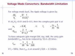
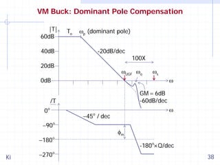
![VM Buck: Loop Gain Function with Rδ
The unity gain frequency fUGF of fs/320 is too low. Fortunately (or
unfortunately), the converter inevitably has parasitic resistors
such as RESR, Rℓ (inductor series resistor), Rs (switch resistance)
and Rd (diode resistance), and the loop gain function is [Ki 98]
T(s)
≈ A(s) ×
where
Rδ
bVo
.
DVm
1
⎛ L
⎞ 2
1+ s⎜
+ CR δ ⎟ + s LC
⎝ RL
⎠
≈ R ESR + R + DR s + D'R d
This Rδ is at least 200mΩ, thus reducing QBCM to around 3. With
GM to be 6dB, fUGF is reduced by 3×2=6 times, and
fUGF
Ki
=
1 fs
f
×
≈ s
6 16 100
If fs=1MHz, then fUGF is at around fs/100 = 10kHz.
37](https://image.slidesharecdn.com/tu0403switcherki2009isic-140305063913-phpapp02/85/IC-Design-of-Power-Management-Circuits-III-37-320.jpg)
![Current Mode Converters: Loop Gain Function
The loop gain function of the buck converter with current mode
control operating in CCM ignoring ESR is given by [Ki 98]
1
1
CR f n1D ' T
T(s) =
⎛ 1
1 ⎞
1 1 ⎛ 1 (n1D '− D)T ⎞
+
+
s2 + s ⎜
⎟ n D' T C ⎜R +
⎟
CR L n1D ' T ⎠
L
⎝
⎝ L
⎠
1
A(s)b ×
with
n1 = 1 +
and
mc
m
2−D
, mc > 2 ⇒ n1 >
m1
2
2D '
R L(BCM) = 2L
D'T
In general, the two poles are real, as discussed next.
Ki
39](https://image.slidesharecdn.com/tu0403switcherki2009isic-140305063913-phpapp02/85/IC-Design-of-Power-Management-Circuits-III-39-320.jpg)