SlideShare a Scribd company logo
1 of 15
Download to read offline
The University of New South Wales
           School of Electrical Engineering and Telecommunications

                 ELEC3017 ELECTRICAL ENGINEERING DESIGN


                    CHAPTER 13: PRINTED CIRCUIT
                          BOARD DESIGN


                                       Lecture Notes Prepared by
           Mr Leon Dearden , Mr Don Williams2 and A/Prof. W.H. Holmes
                                  1


                        (with minor edits by A/Prof. D. Taubman)
                                  1
                                      CLD Quality Services Pty Ltd
                             2
                                 Associative Measurement Pty Ltd.


ELEC3017 Electrical Engineering Design              1                Printed Circuit Board Design
PCB REQUIREMENTS SPECIFICATION

Normally when you contemplate designing a PCB for a particular project, there is the
expectation that there is a need for a number of identical items of product to meet a
customer’s requirements. The customer of course could be internal as well as external.

Whether specified formally or not, there will be a set of requirements that the PCB
assembly is expected to meet. These requirements often cover such things as:
         • Electrical/electronic performance
               ∗   Power output
               ∗   Frequency response
               ∗   Sensitivity
               ∗   Signal to noise ratio
               ∗   Etc.
         • Mechanical
               ∗   Volume, area or height constraints
               ∗   Weight constraints
               ∗   Special shapes to fit in with existing mechanical components
               ∗   Special packaging
               ∗   Etc.
         • Environmental
               ∗   Ambient temperature ranges
               ∗   Humidity
               ∗   Shock and vibration
               ∗   Altitude
               ∗   Etc.

It is important to establish the requirements before circuit design commences, because
often the choice of circuit is very dependant on the type and availability of components
which can meet all of the required performance, mechanical and environmental factors.
There may also be constraints imposed on the design process by the capability of the
available production processes. For example, there may be constraints on the number of
layers 1 , the available hole sizes, the track spacings or finishes. Every effort should be made
to identify constraints on components or processes, including possible trade-offs.


1   Thus, at UNSW only single or double sided boards without plated through holes may be made.


ELEC3017 Electrical Engineering Design                 2                      Printed Circuit Board Design
COMPUTER-AIDED PCB DESIGN PROCEDURE

With the Requirements Specification defined and component and process limitations
understood, it is now time to complete the PCB design. It is assumed in the following that
the electronic circuit design has already been carried out – i.e. the component types and
values have been selected.

PCB design was formerly done by applying opaque tape strips, representing the copper
tracks on the finished PCB, onto a polyester (‘Mylar’) film to produce the ‘artwork’ for the
copper etching. However, nowadays PCBs are almost always designed using special CAD
software packages such as Altiuml, Orcad, Daisy or Mentor, and the artwork is produced
from the resulting computer file using a photoplotter (or perhaps a laser printer or plotter in
less exacting designs).

The steps in the design using PCB design software are generally as follows.


Schematic Entry

The beginning of the design cycle that will result in a PCB is to enter the schematic circuit
design into the CAD system. This process is called “schematic entry” or “schematic
capture”. While it is possible to proceed directly to PCB design without going through the
full schematic capture stage, it is definitely not recommended except for the very simplest
of designs. It is just too easy for humans to fail to detect errors, even in simple PCB
designs.

The PCB schematic entry software has pinout libraries, schematic libraries and function
model libraries for the component parts. Also included is the ability to add your own
components into these libraries. Designs can be done in a hierarchical structure or a
horizontal structure. The hierarchical structure is the best for complicated systems,
including boundaries for VLSI, hybrids (thin and thick film) and special artwork
constructions such as stripline layouts for high frequency work.

There are two main outputs from the schematic entry part of the PCB design software:

      1. The Netlist
         The CAD system will have the necessary connectivity data at the completion of
         the schematic entry process. The most important outcome of the schematic
         capture process is the netlist, which is a file defining the conducting tracks on the
         PCB and their connections to the components. This file is used later to check the
         accuracy of the wiring layout of your PCB, and is also the input to the layout
         stage of the PCB design.

      2. The Parts List or BOM (Bill Of Materials)

         The CAD system will also output a parts list (or Bill of Materials, also known as a
         BOM) after the schematic entry has been completed. Ideally this will interface
         directly to a CAM system, but sometimes small conversion programs are needed
         to convert it into the correct part numbers for the manufacturing data base.


ELEC3017 Electrical Engineering Design          3                    Printed Circuit Board Design
Most schematic capture programs allow you to characterize each component with
         attributes such as component type, style, part number, ratings, supplier etc. This
         makes the production of an accurate parts list a straightforward matter, which is
         important in real-world production situations.


Error Checking

      1. Transcription Errors
         Error checking at this stage is a very important part of the process, as it is during
         the initial circuit entry stage that the greatest potential for human error arises.
         Any error made in transcribing your design will be present in all future stages of
         the process. So check, re-check and check again!
         If you can, get someone else to check your work at this stage to ensure that all
         circuit errors are eliminated.
      2. Other Circuit Errors
         Modern design software tools, such as the Altium tools used in Elec3017, offer
         the facility of an electrical rules check. This check will typically detect shorts,
         inputs with no driving source, unconnected pins, bus contention and a number of
         other common errors.
         Also, the netlist can usually be exported to a circuit analysis program (e.g. SPICE
         or Micro-Cap) to verify the correct electrical operation of the circuit. In fact, the
         Altium software, used in this Elec3017, incorporates its own simulation tools.
         Simulation serves as a final design check, both on the circuit design itself and on
         the schematic entry into the CAD system.
         If the netlist is correct, the final PCB design will also be correct.


Component Placement

The netlist is the input for the actual physical PCB design. The first thing is to place the
components on the PCB. This is the most critical part of the PCB design process,
especially at high frequencies or with high parts densities.


             Design engineers play a much bigger role in component placement
                than in any other aspect of the PCB manufacturing process.


The first operation is to select a basic outline shape for the PCB, and then to manually
place those components whose position is externally constrained (e.g. because of front or
back panel layouts). Other parts may also be placed manually because of design
considerations such as critical track frequencies, bus layouts, thermal geometry, power
supply voltage drop, etc. It is also common to manually place certain major parts, such as
very large ICs. Features such as cut-outs, mounting holes, edge connectors and
mechanical clearance areas are detailed at this stage of the layout.


ELEC3017 Electrical Engineering Design           4                     Printed Circuit Board Design
Many CAD systems can automatically place the remaining components using data from
the netlist to place parts on the PCB outline. The program minimizes conductor lengths,
thus being able to achieve greater parts densities by less track coverage of the available
PCB area. However, many designers prefer not to use automatic placement.


Wiring Connections (Routing)

The next operation is to position (or ‘route’) the conducting tracks between the component
pins. This can also be done automatically by most PCB design programs, but once again
some tracks may first be routed manually for the same reasons that certain components
may be manually placed. In particular, it is usually wise to place power traces and other
critical traces by hand first, especially for audio and RF circuits. Then auto-routing may be
employed if desired, though many designers prefer hand placement of circuit traces.

Be prepared to re-locate components if the trace density is too high or is badly unbalanced
across the area of the board, or if critical leads become too long. The designer should be
aware at all times, particularly with RF designs, that printed wiring has distributed
resistance, inductance and capacitance. The effects of this may have to be allowed for in
the design.

It is important that the manufacturing tolerances (line spacing, conductor width, etc.) are
satisfied – otherwise a PCB design may result that nobody can make. Hence the process
specification has to be known at the PCB layout stage. Most CAD systems differentiate
between bus, track and power conductors. There are also options for minimizing defined
track lengths and assigning connector pinouts to the rest of the system. Multi-PCB
sandwiches (including daughter boards or piggy back boards) can be autorouted and the
autorouter can ‘take over’ at any stage after manual placement and routing.


Design Rule Checks

Once you have completed your layout and interconnections, most PCB design programs
permit you to run design rule checks to ensure that the manufacturing tolerances are
satisfied (e.g. the track width and spacing requirements) and that circuit and signal
connections are correct to the original circuit diagram. This is why the checking applied
to the original circuit schematic is so crucial.

Plotting

The final task is to produce plotted artwork from which the PCBs can be manufactured.
Nowadays it is usually not necessary for a designer to produce the original artwork, as
design files can be transferred to PCB shops as disk files. The PCB shops generally prefer
to produce their own artwork directly from client disk files so that they can ensure the
standard of plotting meets their particular process requirements.

For artwork to be produced, the PCB design has to be converted for photo-tooling. This
implies that the PCB design software must interface with a photoplotter, which is done by
means of a so-called Gerber file. The layers of multilayer PCBs must be suitably defined
as to order, and the dimensions must be defined in relation to a ‘datum point’ (where the


ELEC3017 Electrical Engineering Design         5                    Printed Circuit Board Design
locator awl is later put for the ‘booking’). The details vary from plant to plant. For
example some plants may require negative photo-tooling while others require positive
photo-tooling. The designer today typically produces plots of artwork only for checking or
reference purposes, though in simple manufacturing processes the basic artwork for the
copper etching may be printed using a laser printer or a plotter.


GENERAL PCB DESIGN PRINCIPLES
Determine Your Design Standards

It is now time to determine and set down the design standards that you are going to apply
to the PCB design. More details and options are given below, but an example set of design
standards for a digital logic design may be as follows:
      a) ICs will be logically laid out in an array fashion and oriented east-west on the
         PCB.
      b) Component side traces will run generally east-west with solder-side traces
         running north-south.
      c) IC pads will be oval in shape and 0.050” wide by 0.125” long and allow for
         pin-through connections (see diagram). This will allow one 0.015” wide
         conductor between pads with 0.017” track clearance on each side.
      d) Minimum track widths will be 0.015” and traces will be spaced on a basic 0.050”
         grid.
      e) Power and ground traces shall be 0.050” wide and run east-west between the IC
         pins on the component side of the PCB. These traces shall be connected in a grid
         fashion at the board edges to minimize lead inductances.
      f) 100 nF multilayer ceramic bypass capacitors shall be provided on the basis of one
         per IC package. These capacitors will be located close to each IC package.
      g) IC sockets shall be used and ICs shall be oriented in the same direction.
      h) etc ...


Artwork Viewing Convention

The usual design convention is that layouts are always viewed from the component side of
the board. Adhering to this standard will avoid confusion and possible errors on the part of
board manufacturers.


Component Outlines

At the start of the PCB layout design, select appropriate component outlines from the
component libraries supplied with the PCB design software. Be prepared to modify these
outlines if necessary to conform to your basic design standards. For example, you may
need to adjust the size and orientation of pads to suit non-plated-through designs.


ELEC3017 Electrical Engineering Design         6                    Printed Circuit Board Design
You may also need to create your own outlines if suitable components aren’t available in
the libraries supplied.


Component Placement

Components should always be mounted on the side of the PCB with the least amount of
connecting tracks. If possible, they should be evenly distributed over the PCB. Heavy
components should be placed near board supports whenever possible. The direction of air-
flow and heat-sinking requirements will also influence component placement. The
placement of some components may be externally constrained, e.g., because of front or
back panel layouts. Placement techniques vary depending upon the nature of the circuit
and the preferences or practices of individual designers, but mostly four basic component
placement concepts are used, either independently or in combination:

      1. Schematic Placement
         This is used primarily on low density analogue boards. Where the schematic has
         been drawn with a physical sense and has a minimum of interconnection
         crossovers, components can often be placed more or less as they are physically
         drawn on the circuit diagram. This scheme works particularly well where signal
         inputs can be placed along one edge of a board and the outputs along the opposite
         edge.

      2. Peripheral Placement
         This method is appropriate when board edge connectors or other components that
         require a specific fixed location are used. These components are placed first and
         interconnecting components are placed radiating inwardly from the fixed
         component locations.

      3. Central Placement
         This concept applies to boards that have complex multiple lead devices such as
         integrated circuits, relays or modules with supporting peripheral components. In
         this system, the multi-lead components are centrally placed with the supporting
         components placed radiating outwards from them.
      4. Fixed Arrays
         This concept is typically used for straight digital logic boards comprising mainly
         integrated circuits. Here the ICs are logically placed in fixed patterns with a
         uniform space allotment relating to the number of leads per device.


Wiring and Component Orientation

In general, when locating and orienting components and tracks, strive to achieve an orderly
appearance. The orientation should be made with an eye to logical and short connections.
Components should be placed so that their major axis is parallel to a board edge and to the
flow of cooling air where that is applicable. Also, to the extent that good functional design
is not compromised, components should be placed either parallel (preferable) or at right
angles to each other, and with the same orientations for like components. In particular,


ELEC3017 Electrical Engineering Design         7                    Printed Circuit Board Design
polarized components should all be oriented in the same direction, and value codes and
polarity markings should be visible and readable from the same direction.
On two-layer digital logic boards it is common practice to route all traces on one layer in
one direction, and on the other layer to route all traces in the perpendicular direction. This
scheme requires the use of more feedthroughs or “vias”, but in exchange will provide
maximum routing flexibility, improve reliability, and usually increase circuit packing
density.


6.       SOME PCB DESIGN GUIDELINES
Board Size

There are a number of factors to consider in determining the size of a PCB. First to
consider are any mechanical constraints imposed by the Customer Requirements
Specification – e.g.
         • Dimensional
         • Environmental (heat dissipation, sealing, etc)
         • Incorporation with other mechanical components

Next to consider are any constraints imposed by the available manufacturing process – e.g.
         • Maximum blank sizes
         • Technology (single/double sided, multi-layer, plated-through or non-plated-
           through holes, etc.)

Finally, estimate the area required by the components that have to be mounted, making a
reasonable allowance for the additional area required for connections around integrated
circuits and connectors. As a rule of thumb for a double-sided design, proceed as follows:
         • Compute the square area required for each type of component (including lead
           terminations) and multiply each type by the number of like components (square
           mils is often a convenient unit 2 );
         • For integrated circuits and connectors, use the footprint area (including pins)
           + 50%;
         • Add the area required for board edges (clearances) and mounting hardware and/or
           heatsinks.

If the area required from the above calculations is 80% or less of that available, then the
layout is most likely to be achievable. Anything more than 80% would require a careful
re-assessment and possibly would need a larger board size or a different approach such as
splitting the design into two boards or going to multi-layers.


Conductor Widths and Spacings


2   1 square mil = 0.000001 in2 (i.e. 0.001 in × 0.001 in)


ELEC3017 Electrical Engineering Design                       8      Printed Circuit Board Design
There are a number of factors to be considered when specifying conductor trace widths and
spacings. If a conductor width is too small, the track may become open circuit during or
after manufacture, or there may be heat problems if it carries too much current. However,
it is advisable to avoid using conductors of larger than 0.5” width. If larger areas are
needed, such as for ground planes, then relieved areas should be incorporated to prevent
blistering and warpage during soldering.

Conductor spacing is normally determined by considering peak voltage between
conductors, the altitudes at which the circuit board will be in use, and the conformal
coatings to be applied to the board. Too narrow a spacing between conductors can give
rise to voltage “arc over” or to short circuits due to solder bridging. Generally, excessively
wide widths and spacing can result in waste of space and material and hence unwarranted
cost. The golden rule is to maintain maximum size within the available area, consistent
with maximum trace widths and minimum spacing requirements, to achieve ease of
manufacture and durability in usage.


Conductor Cross Sections

Where current carrying capacity is important, minimum conductor widths and thicknesses
should be checked. It is however often important that the inductance of power reticulation
traces be minimised, e.g., for digital circuit layouts, and this may dictate thicker traces than
those chosen on the basis of current carrying capacity alone.


Conductor Connections and Routing

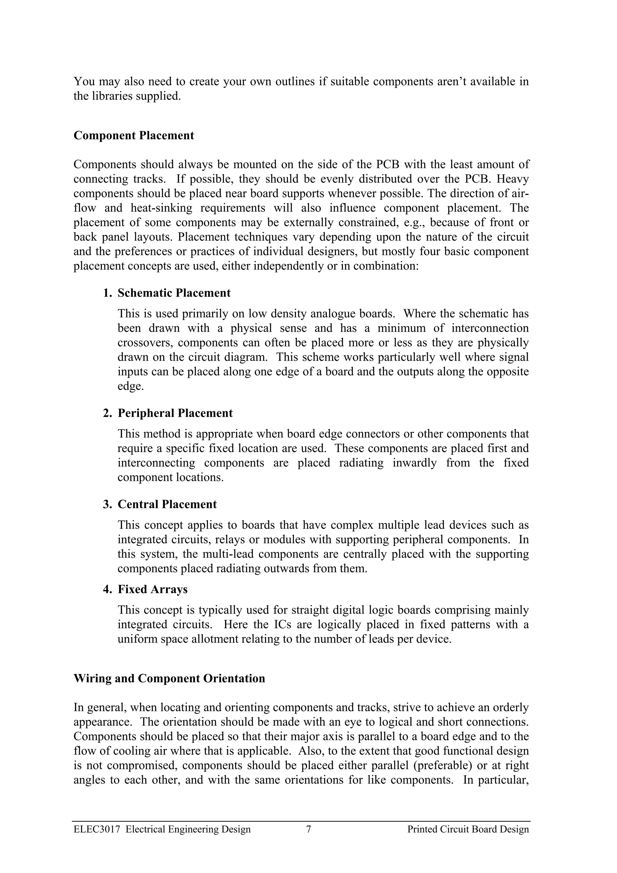
There are some “Dos” and “Don’ts” to be considered when joining traces and when joining
traces to pads. A sample of these are shown in Figure 5.


ELEC3017 Electrical Engineering Design          9                     Printed Circuit Board Design
Figure 5. Connection Dos and Don’ts.


Component Terminal Holes

A printed circuit board should have a separate mounting hole for each component lead or
terminal. The two basic types of terminal holes used are unplated holes and plated-through
holes (PTH). Un-plated or unsupported holes contain no conductive material, plating,
solder or any type of reinforcement. They are usually drilled or punched into a PCB.
Plated-through-holes begin as unsupported holes. Conductive material is then electrically
deposited or “plated” on the inside walls to form an electrical connection between the
layers of a board. The plating usually consists of tin-lead over electro-deposited copper.

For the boards that you will be designing, you will be using unplated holes.

As a guide, the following formula can be used to determine the minimum diameter of an
unplated hole:

         Min. Hole Dia. = Max. Lead Dia. + Min. Drill Tolerance
                          (adjusted to next larger standard drill size)

Typically, minimum drill tolerances are ± 0.003” for holes up to 0.0226” dia. (23 AWG)
and ± 0.004” for larger holes. Table 1 provides a convenient reference. In general,
unplated holes should be no more than 0.020” greater than the minimum lead to be
inserted.

The number of different hole sizes on a circuit board should be kept to a minimum. As the
number of different hole sizes increases, so does the cost and difficulty in manufacturing
the board.


Terminal Areas and Pads

A terminal area or pad is a portion of a printed circuit used for making electrical
connections between a component or wire and part of the conductive circuit pattern.
Generally, pads completely surround and abut the mounting holes. Exceptions are when


ELEC3017 Electrical Engineering Design         10                   Printed Circuit Board Design
“flat pack” type components are to be mounted on the board surface. Terminal area shapes
vary with designer preference, however there are specific advantages and disadvantages to
each particular shape. Square or rectangular shaped pads provide maximum adhesion of
the copper pad to the circuit board and are useful when a large component hole is required
where there is a minimum of useable terminal area space. However, these pads are more
susceptible to solder bridging when placed in close proximity to other pads or traces.
Round or elliptical pads can be placed closer to other pads or traces with less risk of solder
bridging. Terminal area size should be as large as practicable while maintaining minimum
spacing requirements. The minimum pad area is based on:
         1.   The maximum hole size
         2.   Hole location tolerance
         3.   Pad area location tolerance
         4.   Conductor width tolerance
         5.   Minimum required annular ring

Table 1 also shows suggested minimum pad area sizes for various conductor sizes for
unplated holes. Note that these recommendations may need to be modified to suit
particular design requirements, such as running one or more traces between pads or where
a manufacturing process is used that is capable of finer lines and closer tolerances.

Table 1. Hole Sizes and Terminal Areas for Unplated Holes

     Lead Size                              Rec. Hole Size             Rec. Pad Size
     AWG         Dia.           Dia.        Max.                       Pref.    Standard Minimu
                                                          Drill
                 (mm)           (mm)        Tol.                       Pad Dia. Pad Dia. m
                                            (mm)                                         Pad Dia.

     34-29       .160-.287      0.368       0.076         #79          .100”        .075”        .0625”
                                (0.7) *                   (0.7)*

     28-23       .320-.574      0.71        0.076         #70          .115”        .085”        .075”
                                (0.9)*                    (0.9)*

     22-20       .634-.813      1.02        0.102         #60          .125”        .100”        .090”
                                                          (1.0)*

     19-17       .912-1.151 1.32            0.102         #55          .140”        .110”        .100”
                                                          (1.3)*

     16-15       1.29-1.45      1.59        0.102         #52          .150”        .120”        .110”
                                                          (1.6)*


*   Note that the metric sizes shown in brackets are more practical for single and double sided boards of the
    type made at UNSW.


ELEC3017 Electrical Engineering Design                    11                       Printed Circuit Board Design
Dimensions and Tolerances


For more complete information on dimension and tolerance considerations for printed
circuit board design you are referred to the following publications:
            MIL-STD-275D
            MIL-P-13949E
            IPC-ML-910A
            IPC-D-300F
            IPC-D-320A


Ground Planes

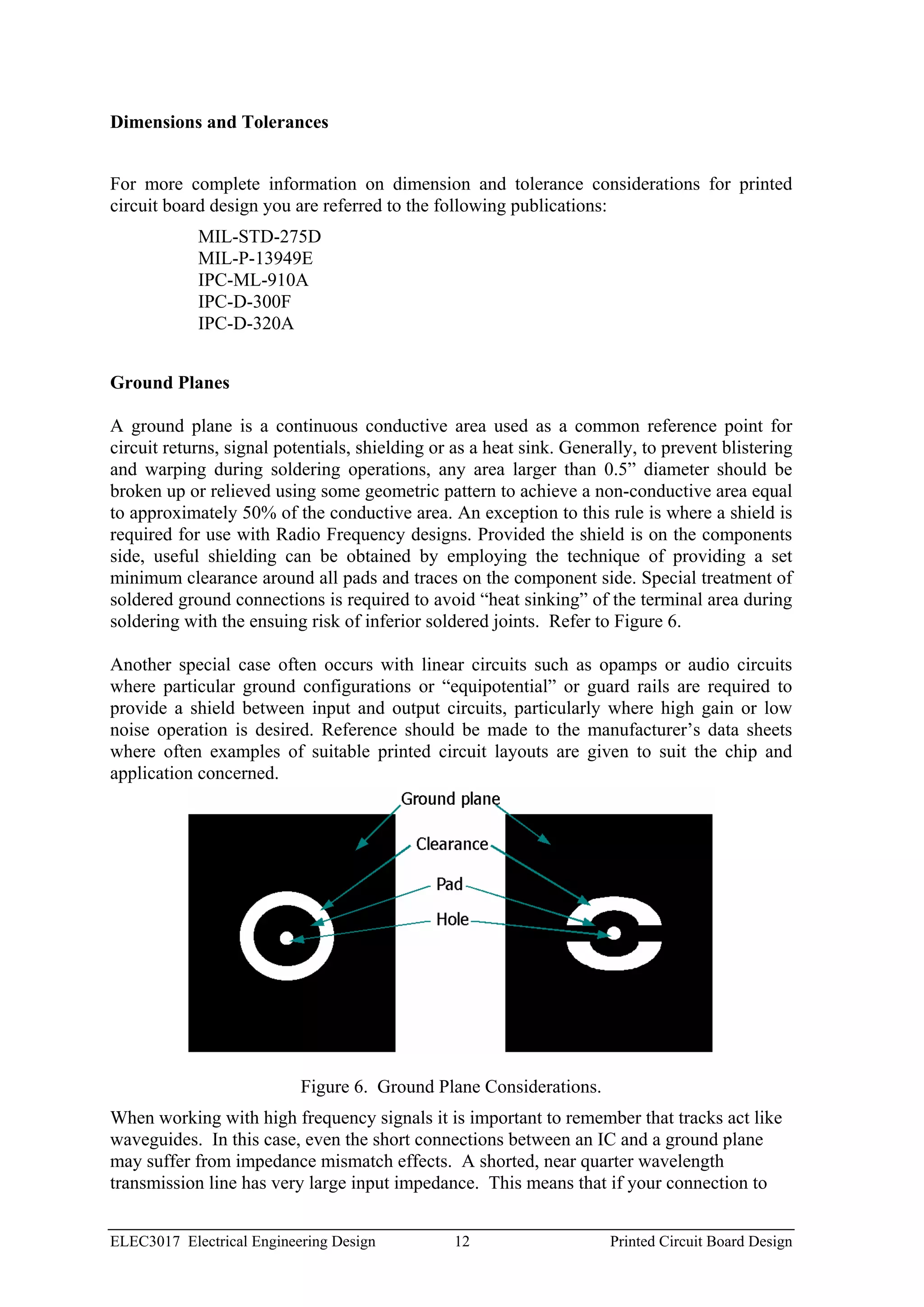
A ground plane is a continuous conductive area used as a common reference point for
circuit returns, signal potentials, shielding or as a heat sink. Generally, to prevent blistering
and warping during soldering operations, any area larger than 0.5” diameter should be
broken up or relieved using some geometric pattern to achieve a non-conductive area equal
to approximately 50% of the conductive area. An exception to this rule is where a shield is
required for use with Radio Frequency designs. Provided the shield is on the components
side, useful shielding can be obtained by employing the technique of providing a set
minimum clearance around all pads and traces on the component side. Special treatment of
soldered ground connections is required to avoid “heat sinking” of the terminal area during
soldering with the ensuing risk of inferior soldered joints. Refer to Figure 6.

Another special case often occurs with linear circuits such as opamps or audio circuits
where particular ground configurations or “equipotential” or guard rails are required to
provide a shield between input and output circuits, particularly where high gain or low
noise operation is desired. Reference should be made to the manufacturer’s data sheets
where often examples of suitable printed circuit layouts are given to suit the chip and
application concerned.


                           Figure 6. Ground Plane Considerations.
When working with high frequency signals it is important to remember that tracks act like
waveguides. In this case, even the short connections between an IC and a ground plane
may suffer from impedance mismatch effects. A shorted, near quarter wavelength
transmission line has very large input impedance. This means that if your connection to


ELEC3017 Electrical Engineering Design          12                     Printed Circuit Board Design
ground is on the order of λ/4, the connection will appear to be very poor indeed. To stay
clear of such problems, it is recommended that connections be no more than λ/20 in length.
At frequencies of 1 MHz, the wavelength is λ≈300 metres, so this is no problem. At
frequencies of 1 GHz, however, the wavelength drops to 300 mm, meaning that you should
try to keep your connections to within about 15 mm in length!!


Inter-Layer Connections in Two-Layer Boards

For two-layer boards, there may not always be the facility for plated-through holes, so that
special consideration will be needed to effect connections between the solder and
component sides of the board. In this situation, the following techniques may be used:
      1. Pin-Throughs
         Arrange opposing pads on both solder and component sides and solder together
         using a wire or special pin made for the purpose (e.g. Harwin pins).
      2. Component Leads
         With forethought many of the component mounting leads can be utilized for
         interlayer connections by soldering the component lead on both sides of the board.
      3. Links or Jumper Wires
         These are particularly useful to bridge data buses or densely populated wiring
         areas. Soldering both sides of the lead also offers interlayer connection
         possibilities.
      4. IC Sockets
         While it is possible to solder both sides of IC pins to effect interlayer connections
         and mimic plated through boards, there is very little chance of successfully
         removing such an IC without damage to the board and the IC, if removal
         subsequently becomes necessary.

For experimental or prototype boards where it is advantageous to be able to remove an IC
for testing or trouble-shooting, it is preferable to use IC sockets. To effect interconnections
between solder and component layers using sockets it is possible to use a double-pad
arrangement, with one pad connected to the socket pin and the other nearby to allow for a
pin through to the other layer. This arrangement can mimic a proper double-sided plated-
through-hole board design quite closely, with a small penalty to pay in terms of extra board
area for pin-throughs.


Component Mounting

Unless required by its function, no part of a component should protrude beyond the edge of
the PCB. Usually a minimum clearance of say 0.062” should be maintained between board
edges and card guides or any other mounting hardware. Components weighing more than 7
grams per lead should be supported by clamps or other means so that soldered joints are
not strained due to shock or vibration effects. All parts dissipating 1 watt or more should
be mounted away from the PCB so that no physical contact is made unless heat sinks are
provided. Any components with conductive cases should ideally be mounted at least
0.062” away from conductive tracks (or more at high voltages or altitudes, or in the

ELEC3017 Electrical Engineering Design         13                    Printed Circuit Board Design
absence of protective coatings). If minimal spacing must be used then some form of
additional insulation is required. Horizontally mounted axial lead components should be
mounted with the body of the part in contact with the PCB and clamped if the weight is
above that specified above. If axial components are to be mounted vertically then they
should be spaced around 0.015” (min.) to 0.125” (max.) above the PCB to allow for good
soldered joints and adequate cleaning. The highest point of the top lead should not extend
more than 0.550” above the board surface and may need to be insulated to prevent contact
with other components. The same comments regarding weight apply here.

There are a number of recommendations from both IPC and MIL-STD about lead spacing
of axial lead components. In general it is recommended that axial leads extend around
0.060” straight out from the body of the component before the bend starts and that the
minimum bend radius should be one to two times the wire diameter. To determine the
minimum lead spacing, use the following formula:

                          LSmin = CLmax + 2 × LE + 2 × BRmin + LD
where:
      LS    = Lead spacing (rounded up to the nearest standard grid increment).
      CLmax = Maximum component length (including coating meniscus or other
              excrescences).
      LE    = Lead extension (0.030” min. to 0.060” preferred).
      LD    = Lead diameter.
      BRmin = Minimum bend radius, calculated as follows:


                        Condition                   BRmin
                        LD < 0.027”                 1 × LD
                        0.028” < LD < 0.047”        1.5 × LD
                        0.047” < LD                 2 × LD


Automatic Component Insertion and Surface Mounted Components

Most of the foregoing is applicable for all types of PCBs, although the emphasis was on
through-hole technology. However, there are additional factors to be considered when a
board is being designed for automatic (NC) component insertion and/or for use with
surface mounted components. We will not go into these here, but if this is contemplated in
future, then it would be advisable to obtain advice on layout requirements from the
particular board manufacturer before commencing the layout.


ELEC3017 Electrical Engineering Design         14                   Printed Circuit Board Design
REFERENCES
[1]      K. Brindley, Newnes Electronics Assembly Handbook, Butterworth-Heinemann,
         Oxford, 1993.
[2]      Printed Circuit Drafting Technical Manual and Catalog 107A, Bishop Graphics,
         1985. This is unfortunately now out of print, but all the relevant information
         originated from the IPC and MIL references which follow.
[3]      Guide to Making Printed Circuit Boards, Dick Smith Electronics, Cat B-6005.
[4]      Definitions and Terms:
                MIL-STD-429 Printed Wiring and Printed Circuit Terms and Definitions.
                IPC-T-50 Terms and Definitions
[5]      Printed Circuit Design – Single-Sided and Two-Sided Boards:
                MIL-STD-275D, Printed Wiring.
                MIL-P-55110, Printed Wiring Boards.
                IPC-D-300, Printed Wiring Board Dimensions and Tolerances 3.
                IPC-CM-770, Guidelines for Printed Circuit Board Component Mounting.


3   IPC stands for Institute for Interconnecting & Packaging Electronic Circuits, Evanston, IL USA.


ELEC3017 Electrical Engineering Design                  15                       Printed Circuit Board Design

More Related Content

What's hot

minimisation of crosstalk in VLSI routing
minimisation of crosstalk in VLSI routingminimisation of crosstalk in VLSI routing
minimisation of crosstalk in VLSI routingChandrajit Pal
 
Printed board circuit design (Pcb) PPT
 Printed board circuit design (Pcb) PPT Printed board circuit design (Pcb) PPT
Printed board circuit design (Pcb) PPTHoneyKumar34
 
Pcb manufacturing
Pcb manufacturingPcb manufacturing
Pcb manufacturingClement Ang
 
Introduction to PCB Designing
Introduction to PCB DesigningIntroduction to PCB Designing
Introduction to PCB DesigningSharan kumar
 
pcb layers in layout
pcb layers in layoutpcb layers in layout
pcb layers in layoutAnum Mairaj
 
Design of Printed Circuit Boards
Design of Printed Circuit BoardsDesign of Printed Circuit Boards
Design of Printed Circuit BoardsChandana129742
 
Printed Circuit Board Basics
Printed Circuit Board BasicsPrinted Circuit Board Basics
Printed Circuit Board BasicsSierra Assembly
 
crosstalk minimisation using vlsi
crosstalk minimisation using vlsicrosstalk minimisation using vlsi
crosstalk minimisation using vlsisubhradeep mitra
 
PCB DESIGNING & MANUFACTURING
PCB DESIGNING & MANUFACTURING PCB DESIGNING & MANUFACTURING
PCB DESIGNING & MANUFACTURING prasanna kumar
 
Nanometer layout handbook at high speed design
Nanometer layout handbook at high speed designNanometer layout handbook at high speed design
Nanometer layout handbook at high speed designMinho Park
 
Packaging of vlsi devices
Packaging of vlsi devicesPackaging of vlsi devices
Packaging of vlsi devicesAshu0711
 
Surface mount Devices(SMD)
Surface mount Devices(SMD)Surface mount Devices(SMD)
Surface mount Devices(SMD)shyamaliamale
 

What's hot (20)

PCB Layout Fundamentals
PCB Layout FundamentalsPCB Layout Fundamentals
PCB Layout Fundamentals
 
minimisation of crosstalk in VLSI routing
minimisation of crosstalk in VLSI routingminimisation of crosstalk in VLSI routing
minimisation of crosstalk in VLSI routing
 
Printed board circuit design (Pcb) PPT
 Printed board circuit design (Pcb) PPT Printed board circuit design (Pcb) PPT
Printed board circuit design (Pcb) PPT
 
WelcomePCB
WelcomePCBWelcomePCB
WelcomePCB
 
Pcb design powerpoint
Pcb design powerpointPcb design powerpoint
Pcb design powerpoint
 
Pcb designing
Pcb designingPcb designing
Pcb designing
 
Pcb manufacturing
Pcb manufacturingPcb manufacturing
Pcb manufacturing
 
Introduction to PCB Designing
Introduction to PCB DesigningIntroduction to PCB Designing
Introduction to PCB Designing
 
PCB Designing
PCB Designing PCB Designing
PCB Designing
 
pcb layers in layout
pcb layers in layoutpcb layers in layout
pcb layers in layout
 
Pcb layout
Pcb layoutPcb layout
Pcb layout
 
Design of Printed Circuit Boards
Design of Printed Circuit BoardsDesign of Printed Circuit Boards
Design of Printed Circuit Boards
 
Printed Circuit Board Basics
Printed Circuit Board BasicsPrinted Circuit Board Basics
Printed Circuit Board Basics
 
crosstalk minimisation using vlsi
crosstalk minimisation using vlsicrosstalk minimisation using vlsi
crosstalk minimisation using vlsi
 
PCB DESIGNING & MANUFACTURING
PCB DESIGNING & MANUFACTURING PCB DESIGNING & MANUFACTURING
PCB DESIGNING & MANUFACTURING
 
Nanometer layout handbook at high speed design
Nanometer layout handbook at high speed designNanometer layout handbook at high speed design
Nanometer layout handbook at high speed design
 
Packaging of vlsi devices
Packaging of vlsi devicesPackaging of vlsi devices
Packaging of vlsi devices
 
Surface mount Devices(SMD)
Surface mount Devices(SMD)Surface mount Devices(SMD)
Surface mount Devices(SMD)
 
PCB DESIGN - Introduction to PCB Design Manufacturing
PCB DESIGN - Introduction to PCB Design ManufacturingPCB DESIGN - Introduction to PCB Design Manufacturing
PCB DESIGN - Introduction to PCB Design Manufacturing
 
Pcb designing
Pcb designingPcb designing
Pcb designing
 

Viewers also liked

Puppet modules: An Holistic Approach
Puppet modules: An Holistic ApproachPuppet modules: An Holistic Approach
Puppet modules: An Holistic ApproachAlessandro Franceschi
 
Hardware 1 pandhu
Hardware 1 pandhu Hardware 1 pandhu
Hardware 1 pandhu pandhuputra
 
Panduan mesin cnc hurco vmx 24
Panduan mesin cnc hurco vmx 24Panduan mesin cnc hurco vmx 24
Panduan mesin cnc hurco vmx 24Zul Abidin
 
080930 Ipc 2152 Standard For Determining Current Carrying Capacity
080930 Ipc 2152 Standard For Determining Current Carrying Capacity080930 Ipc 2152 Standard For Determining Current Carrying Capacity
080930 Ipc 2152 Standard For Determining Current Carrying Capacityljh1680
 
Programming embedded system_ii_keil_8051(1)
Programming embedded system_ii_keil_8051(1)Programming embedded system_ii_keil_8051(1)
Programming embedded system_ii_keil_8051(1)Fendie Mimpi
 
C presentation book
C presentation bookC presentation book
C presentation bookkrunal1210
 
Automotive Circuit Boards
Automotive Circuit BoardsAutomotive Circuit Boards
Automotive Circuit BoardsArt Wood
 
RoHS Compliant Lead Free PCB Fabrication
RoHS Compliant Lead Free PCB FabricationRoHS Compliant Lead Free PCB Fabrication
RoHS Compliant Lead Free PCB FabricationArt Wood
 
Pcb Production and Prototype Manufacturing Capabilities for Saturn Electronic...
Pcb Production and Prototype Manufacturing Capabilities for Saturn Electronic...Pcb Production and Prototype Manufacturing Capabilities for Saturn Electronic...
Pcb Production and Prototype Manufacturing Capabilities for Saturn Electronic...Art Wood
 
training_presentation
training_presentationtraining_presentation
training_presentationAniket Pawar
 
Epoxy flux a low cost high reliability approach for pop assembly-imaps 2011
Epoxy flux  a low cost high reliability approach for pop assembly-imaps 2011Epoxy flux  a low cost high reliability approach for pop assembly-imaps 2011
Epoxy flux a low cost high reliability approach for pop assembly-imaps 2011nclee715
 
New Algorithms to Improve X-Ray Inspection
New Algorithms to Improve X-Ray InspectionNew Algorithms to Improve X-Ray Inspection
New Algorithms to Improve X-Ray InspectionBill Cardoso
 
A solder joint reliability model for the philips lumileds luxeon rebel led c...
A solder joint reliability model for the philips lumileds luxeon rebel led  c...A solder joint reliability model for the philips lumileds luxeon rebel led  c...
A solder joint reliability model for the philips lumileds luxeon rebel led c...Greg Caswell
 
Managing input and output operation in c
Managing input and output operation in cManaging input and output operation in c
Managing input and output operation in cyazad dumasia
 

Viewers also liked (20)

Puppet modules: An Holistic Approach
Puppet modules: An Holistic ApproachPuppet modules: An Holistic Approach
Puppet modules: An Holistic Approach
 
Hardware 1 pandhu
Hardware 1 pandhu Hardware 1 pandhu
Hardware 1 pandhu
 
Design 2
Design 2Design 2
Design 2
 
Panduan mesin cnc hurco vmx 24
Panduan mesin cnc hurco vmx 24Panduan mesin cnc hurco vmx 24
Panduan mesin cnc hurco vmx 24
 
080930 Ipc 2152 Standard For Determining Current Carrying Capacity
080930 Ipc 2152 Standard For Determining Current Carrying Capacity080930 Ipc 2152 Standard For Determining Current Carrying Capacity
080930 Ipc 2152 Standard For Determining Current Carrying Capacity
 
PCB DESIGN - Introduction to PCB Design Library Creation
PCB DESIGN -  Introduction to PCB Design Library Creation PCB DESIGN -  Introduction to PCB Design Library Creation
PCB DESIGN - Introduction to PCB Design Library Creation
 
Programming embedded system_ii_keil_8051(1)
Programming embedded system_ii_keil_8051(1)Programming embedded system_ii_keil_8051(1)
Programming embedded system_ii_keil_8051(1)
 
C presentation book
C presentation bookC presentation book
C presentation book
 
Automotive Circuit Boards
Automotive Circuit BoardsAutomotive Circuit Boards
Automotive Circuit Boards
 
RoHS Compliant Lead Free PCB Fabrication
RoHS Compliant Lead Free PCB FabricationRoHS Compliant Lead Free PCB Fabrication
RoHS Compliant Lead Free PCB Fabrication
 
How To Design PCB
How To Design PCBHow To Design PCB
How To Design PCB
 
SMT machine Training Manual for FUJI CP6 Series Level 3
SMT machine Training Manual for FUJI  CP6 Series Level 3SMT machine Training Manual for FUJI  CP6 Series Level 3
SMT machine Training Manual for FUJI CP6 Series Level 3
 
Pcb Production and Prototype Manufacturing Capabilities for Saturn Electronic...
Pcb Production and Prototype Manufacturing Capabilities for Saturn Electronic...Pcb Production and Prototype Manufacturing Capabilities for Saturn Electronic...
Pcb Production and Prototype Manufacturing Capabilities for Saturn Electronic...
 
Reflow oven
Reflow ovenReflow oven
Reflow oven
 
training_presentation
training_presentationtraining_presentation
training_presentation
 
Epoxy flux a low cost high reliability approach for pop assembly-imaps 2011
Epoxy flux  a low cost high reliability approach for pop assembly-imaps 2011Epoxy flux  a low cost high reliability approach for pop assembly-imaps 2011
Epoxy flux a low cost high reliability approach for pop assembly-imaps 2011
 
New Algorithms to Improve X-Ray Inspection
New Algorithms to Improve X-Ray InspectionNew Algorithms to Improve X-Ray Inspection
New Algorithms to Improve X-Ray Inspection
 
PIC_ARM_AVR
PIC_ARM_AVRPIC_ARM_AVR
PIC_ARM_AVR
 
A solder joint reliability model for the philips lumileds luxeon rebel led c...
A solder joint reliability model for the philips lumileds luxeon rebel led  c...A solder joint reliability model for the philips lumileds luxeon rebel led  c...
A solder joint reliability model for the philips lumileds luxeon rebel led c...
 
Managing input and output operation in c
Managing input and output operation in cManaging input and output operation in c
Managing input and output operation in c
 

Similar to Chapter13 pcb design

Implementing the latest embedded component technology from concept-to-manufac...
Implementing the latest embedded component technology from concept-to-manufac...Implementing the latest embedded component technology from concept-to-manufac...
Implementing the latest embedded component technology from concept-to-manufac...Zuken
 
Electronic circuit design and component selection.pptx
Electronic circuit design and component selection.pptxElectronic circuit design and component selection.pptx
Electronic circuit design and component selection.pptxmaheshmp16
 
Pcb design using_eagle
Pcb design using_eaglePcb design using_eagle
Pcb design using_eagleABDUL MUNAFF
 
Complete overview of the circuit board fabrication procedure
Complete overview of the circuit board fabrication procedureComplete overview of the circuit board fabrication procedure
Complete overview of the circuit board fabrication procedureShax Engineering, Inc.
 
PCB Fabrication, China PCB Circuit Board Manufacturing from China
PCB Fabrication, China PCB Circuit Board Manufacturing from ChinaPCB Fabrication, China PCB Circuit Board Manufacturing from China
PCB Fabrication, China PCB Circuit Board Manufacturing from ChinaLeah-Hitech PCB
 
IC reverse engineering
IC reverse engineeringIC reverse engineering
IC reverse engineeringhelloseo1
 
EELE 5331 Digital ASIC DesignLab ManualDr. Yushi Zhou.docx
EELE 5331 Digital ASIC DesignLab ManualDr. Yushi Zhou.docxEELE 5331 Digital ASIC DesignLab ManualDr. Yushi Zhou.docx
EELE 5331 Digital ASIC DesignLab ManualDr. Yushi Zhou.docxtoltonkendal
 
Design & simulation capability
Design & simulation capabilityDesign & simulation capability
Design & simulation capabilityrogercooke
 
Chandan Kumar_3+_Years _EXP
Chandan Kumar_3+_Years _EXPChandan Kumar_3+_Years _EXP
Chandan Kumar_3+_Years _EXPChandan kumar
 
Chapter12 manufacturing-processes
Chapter12 manufacturing-processesChapter12 manufacturing-processes
Chapter12 manufacturing-processesVin Voro
 
PCB Terminologies in PCB designing
PCB Terminologies in PCB designingPCB Terminologies in PCB designing
PCB Terminologies in PCB designingMSHOAIBASLAM1
 
Analysis Guide for Electronics / Electrical Product Designers
Analysis Guide for Electronics / Electrical Product DesignersAnalysis Guide for Electronics / Electrical Product Designers
Analysis Guide for Electronics / Electrical Product DesignersSOLIDWORKS
 

Similar to Chapter13 pcb design (20)

Implementing the latest embedded component technology from concept-to-manufac...
Implementing the latest embedded component technology from concept-to-manufac...Implementing the latest embedded component technology from concept-to-manufac...
Implementing the latest embedded component technology from concept-to-manufac...
 
Electronic circuit design and component selection.pptx
Electronic circuit design and component selection.pptxElectronic circuit design and component selection.pptx
Electronic circuit design and component selection.pptx
 
Pcb design using_eagle
Pcb design using_eaglePcb design using_eagle
Pcb design using_eagle
 
Complete overview of the circuit board fabrication procedure
Complete overview of the circuit board fabrication procedureComplete overview of the circuit board fabrication procedure
Complete overview of the circuit board fabrication procedure
 
PCB Fabrication, China PCB Circuit Board Manufacturing from China
PCB Fabrication, China PCB Circuit Board Manufacturing from ChinaPCB Fabrication, China PCB Circuit Board Manufacturing from China
PCB Fabrication, China PCB Circuit Board Manufacturing from China
 
PCB Assembly Manufacturer Hitech circuits
PCB Assembly Manufacturer Hitech circuitsPCB Assembly Manufacturer Hitech circuits
PCB Assembly Manufacturer Hitech circuits
 
ORCAD pcb design
ORCAD pcb designORCAD pcb design
ORCAD pcb design
 
PCB desine final.pdf
PCB desine final.pdfPCB desine final.pdf
PCB desine final.pdf
 
IC reverse engineering
IC reverse engineeringIC reverse engineering
IC reverse engineering
 
EELE 5331 Digital ASIC DesignLab ManualDr. Yushi Zhou.docx
EELE 5331 Digital ASIC DesignLab ManualDr. Yushi Zhou.docxEELE 5331 Digital ASIC DesignLab ManualDr. Yushi Zhou.docx
EELE 5331 Digital ASIC DesignLab ManualDr. Yushi Zhou.docx
 
PCB fabrication.pptx
PCB fabrication.pptxPCB fabrication.pptx
PCB fabrication.pptx
 
Digital_system_design_A (1).ppt
Digital_system_design_A (1).pptDigital_system_design_A (1).ppt
Digital_system_design_A (1).ppt
 
Design & simulation capability
Design & simulation capabilityDesign & simulation capability
Design & simulation capability
 
Lvs
LvsLvs
Lvs
 
Chandan Kumar_3+_Years _EXP
Chandan Kumar_3+_Years _EXPChandan Kumar_3+_Years _EXP
Chandan Kumar_3+_Years _EXP
 
Chapter1.slides
Chapter1.slidesChapter1.slides
Chapter1.slides
 
Chapter12.pdf
Chapter12.pdfChapter12.pdf
Chapter12.pdf
 
Chapter12 manufacturing-processes
Chapter12 manufacturing-processesChapter12 manufacturing-processes
Chapter12 manufacturing-processes
 
PCB Terminologies in PCB designing
PCB Terminologies in PCB designingPCB Terminologies in PCB designing
PCB Terminologies in PCB designing
 
Analysis Guide for Electronics / Electrical Product Designers
Analysis Guide for Electronics / Electrical Product DesignersAnalysis Guide for Electronics / Electrical Product Designers
Analysis Guide for Electronics / Electrical Product Designers
 

More from Vin Voro

Tele3113 tut6
Tele3113 tut6Tele3113 tut6
Tele3113 tut6Vin Voro
 
Tele3113 tut5
Tele3113 tut5Tele3113 tut5
Tele3113 tut5Vin Voro
 
Tele3113 tut4
Tele3113 tut4Tele3113 tut4
Tele3113 tut4Vin Voro
 
Tele3113 tut1
Tele3113 tut1Tele3113 tut1
Tele3113 tut1Vin Voro
 
Tele3113 tut3
Tele3113 tut3Tele3113 tut3
Tele3113 tut3Vin Voro
 
Tele3113 tut2
Tele3113 tut2Tele3113 tut2
Tele3113 tut2Vin Voro
 
Tele3113 wk11tue
Tele3113 wk11tueTele3113 wk11tue
Tele3113 wk11tueVin Voro
 
Tele3113 wk10wed
Tele3113 wk10wedTele3113 wk10wed
Tele3113 wk10wedVin Voro
 
Tele3113 wk10tue
Tele3113 wk10tueTele3113 wk10tue
Tele3113 wk10tueVin Voro
 
Tele3113 wk11wed
Tele3113 wk11wedTele3113 wk11wed
Tele3113 wk11wedVin Voro
 
Tele3113 wk7wed
Tele3113 wk7wedTele3113 wk7wed
Tele3113 wk7wedVin Voro
 
Tele3113 wk9tue
Tele3113 wk9tueTele3113 wk9tue
Tele3113 wk9tueVin Voro
 
Tele3113 wk8wed
Tele3113 wk8wedTele3113 wk8wed
Tele3113 wk8wedVin Voro
 
Tele3113 wk9wed
Tele3113 wk9wedTele3113 wk9wed
Tele3113 wk9wedVin Voro
 
Tele3113 wk7wed
Tele3113 wk7wedTele3113 wk7wed
Tele3113 wk7wedVin Voro
 
Tele3113 wk7wed
Tele3113 wk7wedTele3113 wk7wed
Tele3113 wk7wedVin Voro
 
Tele3113 wk7tue
Tele3113 wk7tueTele3113 wk7tue
Tele3113 wk7tueVin Voro
 
Tele3113 wk6wed
Tele3113 wk6wedTele3113 wk6wed
Tele3113 wk6wedVin Voro
 
Tele3113 wk6tue
Tele3113 wk6tueTele3113 wk6tue
Tele3113 wk6tueVin Voro
 
Tele3113 wk5tue
Tele3113 wk5tueTele3113 wk5tue
Tele3113 wk5tueVin Voro
 

More from Vin Voro (20)

Tele3113 tut6
Tele3113 tut6Tele3113 tut6
Tele3113 tut6
 
Tele3113 tut5
Tele3113 tut5Tele3113 tut5
Tele3113 tut5
 
Tele3113 tut4
Tele3113 tut4Tele3113 tut4
Tele3113 tut4
 
Tele3113 tut1
Tele3113 tut1Tele3113 tut1
Tele3113 tut1
 
Tele3113 tut3
Tele3113 tut3Tele3113 tut3
Tele3113 tut3
 
Tele3113 tut2
Tele3113 tut2Tele3113 tut2
Tele3113 tut2
 
Tele3113 wk11tue
Tele3113 wk11tueTele3113 wk11tue
Tele3113 wk11tue
 
Tele3113 wk10wed
Tele3113 wk10wedTele3113 wk10wed
Tele3113 wk10wed
 
Tele3113 wk10tue
Tele3113 wk10tueTele3113 wk10tue
Tele3113 wk10tue
 
Tele3113 wk11wed
Tele3113 wk11wedTele3113 wk11wed
Tele3113 wk11wed
 
Tele3113 wk7wed
Tele3113 wk7wedTele3113 wk7wed
Tele3113 wk7wed
 
Tele3113 wk9tue
Tele3113 wk9tueTele3113 wk9tue
Tele3113 wk9tue
 
Tele3113 wk8wed
Tele3113 wk8wedTele3113 wk8wed
Tele3113 wk8wed
 
Tele3113 wk9wed
Tele3113 wk9wedTele3113 wk9wed
Tele3113 wk9wed
 
Tele3113 wk7wed
Tele3113 wk7wedTele3113 wk7wed
Tele3113 wk7wed
 
Tele3113 wk7wed
Tele3113 wk7wedTele3113 wk7wed
Tele3113 wk7wed
 
Tele3113 wk7tue
Tele3113 wk7tueTele3113 wk7tue
Tele3113 wk7tue
 
Tele3113 wk6wed
Tele3113 wk6wedTele3113 wk6wed
Tele3113 wk6wed
 
Tele3113 wk6tue
Tele3113 wk6tueTele3113 wk6tue
Tele3113 wk6tue
 
Tele3113 wk5tue
Tele3113 wk5tueTele3113 wk5tue
Tele3113 wk5tue
 

Recently uploaded

Contemporary philippine arts from the regions_PPT_Module_12 [Autosaved] (1).pptx
Contemporary philippine arts from the regions_PPT_Module_12 [Autosaved] (1).pptxContemporary philippine arts from the regions_PPT_Module_12 [Autosaved] (1).pptx
Contemporary philippine arts from the regions_PPT_Module_12 [Autosaved] (1).pptxRoyAbrique
 
call girls in Kamla Market (DELHI) 🔝 >༒9953330565🔝 genuine Escort Service 🔝✔️✔️
call girls in Kamla Market (DELHI) 🔝 >༒9953330565🔝 genuine Escort Service 🔝✔️✔️call girls in Kamla Market (DELHI) 🔝 >༒9953330565🔝 genuine Escort Service 🔝✔️✔️
call girls in Kamla Market (DELHI) 🔝 >༒9953330565🔝 genuine Escort Service 🔝✔️✔️9953056974 Low Rate Call Girls In Saket, Delhi NCR
 
The basics of sentences session 2pptx copy.pptx
The basics of sentences session 2pptx copy.pptxThe basics of sentences session 2pptx copy.pptx
The basics of sentences session 2pptx copy.pptxheathfieldcps1
 
Introduction to AI in Higher Education_draft.pptx
Introduction to AI in Higher Education_draft.pptxIntroduction to AI in Higher Education_draft.pptx
Introduction to AI in Higher Education_draft.pptxpboyjonauth
 
Science 7 - LAND and SEA BREEZE and its Characteristics
Science 7 - LAND and SEA BREEZE and its CharacteristicsScience 7 - LAND and SEA BREEZE and its Characteristics
Science 7 - LAND and SEA BREEZE and its CharacteristicsKarinaGenton
 
Solving Puzzles Benefits Everyone (English).pptx
Solving Puzzles Benefits Everyone (English).pptxSolving Puzzles Benefits Everyone (English).pptx
Solving Puzzles Benefits Everyone (English).pptxOH TEIK BIN
 
Call Girls in Dwarka Mor Delhi Contact Us 9654467111
Call Girls in Dwarka Mor Delhi Contact Us 9654467111Call Girls in Dwarka Mor Delhi Contact Us 9654467111
Call Girls in Dwarka Mor Delhi Contact Us 9654467111Sapana Sha
 
Interactive Powerpoint_How to Master effective communication
Interactive Powerpoint_How to Master effective communicationInteractive Powerpoint_How to Master effective communication
Interactive Powerpoint_How to Master effective communicationnomboosow
 
Alper Gobel In Media Res Media Component
Alper Gobel In Media Res Media ComponentAlper Gobel In Media Res Media Component
Alper Gobel In Media Res Media ComponentInMediaRes1
 
How to Configure Email Server in Odoo 17
How to Configure Email Server in Odoo 17How to Configure Email Server in Odoo 17
How to Configure Email Server in Odoo 17Celine George
 
POINT- BIOCHEMISTRY SEM 2 ENZYMES UNIT 5.pptx
POINT- BIOCHEMISTRY SEM 2 ENZYMES UNIT 5.pptxPOINT- BIOCHEMISTRY SEM 2 ENZYMES UNIT 5.pptx
POINT- BIOCHEMISTRY SEM 2 ENZYMES UNIT 5.pptxSayali Powar
 
Hybridoma Technology ( Production , Purification , and Application )
Hybridoma Technology  ( Production , Purification , and Application  ) Hybridoma Technology  ( Production , Purification , and Application  )
Hybridoma Technology ( Production , Purification , and Application ) Sakshi Ghasle
 
Organic Name Reactions for the students and aspirants of Chemistry12th.pptx
Organic Name Reactions  for the students and aspirants of Chemistry12th.pptxOrganic Name Reactions  for the students and aspirants of Chemistry12th.pptx
Organic Name Reactions for the students and aspirants of Chemistry12th.pptxVS Mahajan Coaching Centre
 
Software Engineering Methodologies (overview)
Software Engineering Methodologies (overview)Software Engineering Methodologies (overview)
Software Engineering Methodologies (overview)eniolaolutunde
 
ECONOMIC CONTEXT - LONG FORM TV DRAMA - PPT
ECONOMIC CONTEXT - LONG FORM TV DRAMA - PPTECONOMIC CONTEXT - LONG FORM TV DRAMA - PPT
ECONOMIC CONTEXT - LONG FORM TV DRAMA - PPTiammrhaywood
 
BASLIQ CURRENT LOOKBOOK LOOKBOOK(1) (1).pdf
BASLIQ CURRENT LOOKBOOK  LOOKBOOK(1) (1).pdfBASLIQ CURRENT LOOKBOOK  LOOKBOOK(1) (1).pdf
BASLIQ CURRENT LOOKBOOK LOOKBOOK(1) (1).pdfSoniaTolstoy
 
The Most Excellent Way | 1 Corinthians 13
The Most Excellent Way | 1 Corinthians 13The Most Excellent Way | 1 Corinthians 13
The Most Excellent Way | 1 Corinthians 13Steve Thomason
 
How to Make a Pirate ship Primary Education.pptx
How to Make a Pirate ship Primary Education.pptxHow to Make a Pirate ship Primary Education.pptx
How to Make a Pirate ship Primary Education.pptxmanuelaromero2013
 

Recently uploaded (20)

Contemporary philippine arts from the regions_PPT_Module_12 [Autosaved] (1).pptx
Contemporary philippine arts from the regions_PPT_Module_12 [Autosaved] (1).pptxContemporary philippine arts from the regions_PPT_Module_12 [Autosaved] (1).pptx
Contemporary philippine arts from the regions_PPT_Module_12 [Autosaved] (1).pptx
 
call girls in Kamla Market (DELHI) 🔝 >༒9953330565🔝 genuine Escort Service 🔝✔️✔️
call girls in Kamla Market (DELHI) 🔝 >༒9953330565🔝 genuine Escort Service 🔝✔️✔️call girls in Kamla Market (DELHI) 🔝 >༒9953330565🔝 genuine Escort Service 🔝✔️✔️
call girls in Kamla Market (DELHI) 🔝 >༒9953330565🔝 genuine Escort Service 🔝✔️✔️
 
The basics of sentences session 2pptx copy.pptx
The basics of sentences session 2pptx copy.pptxThe basics of sentences session 2pptx copy.pptx
The basics of sentences session 2pptx copy.pptx
 
Introduction to AI in Higher Education_draft.pptx
Introduction to AI in Higher Education_draft.pptxIntroduction to AI in Higher Education_draft.pptx
Introduction to AI in Higher Education_draft.pptx
 
Science 7 - LAND and SEA BREEZE and its Characteristics
Science 7 - LAND and SEA BREEZE and its CharacteristicsScience 7 - LAND and SEA BREEZE and its Characteristics
Science 7 - LAND and SEA BREEZE and its Characteristics
 
Solving Puzzles Benefits Everyone (English).pptx
Solving Puzzles Benefits Everyone (English).pptxSolving Puzzles Benefits Everyone (English).pptx
Solving Puzzles Benefits Everyone (English).pptx
 
Call Girls in Dwarka Mor Delhi Contact Us 9654467111
Call Girls in Dwarka Mor Delhi Contact Us 9654467111Call Girls in Dwarka Mor Delhi Contact Us 9654467111
Call Girls in Dwarka Mor Delhi Contact Us 9654467111
 
Interactive Powerpoint_How to Master effective communication
Interactive Powerpoint_How to Master effective communicationInteractive Powerpoint_How to Master effective communication
Interactive Powerpoint_How to Master effective communication
 
Alper Gobel In Media Res Media Component
Alper Gobel In Media Res Media ComponentAlper Gobel In Media Res Media Component
Alper Gobel In Media Res Media Component
 
How to Configure Email Server in Odoo 17
How to Configure Email Server in Odoo 17How to Configure Email Server in Odoo 17
How to Configure Email Server in Odoo 17
 
POINT- BIOCHEMISTRY SEM 2 ENZYMES UNIT 5.pptx
POINT- BIOCHEMISTRY SEM 2 ENZYMES UNIT 5.pptxPOINT- BIOCHEMISTRY SEM 2 ENZYMES UNIT 5.pptx
POINT- BIOCHEMISTRY SEM 2 ENZYMES UNIT 5.pptx
 
Hybridoma Technology ( Production , Purification , and Application )
Hybridoma Technology  ( Production , Purification , and Application  ) Hybridoma Technology  ( Production , Purification , and Application  )
Hybridoma Technology ( Production , Purification , and Application )
 
Organic Name Reactions for the students and aspirants of Chemistry12th.pptx
Organic Name Reactions  for the students and aspirants of Chemistry12th.pptxOrganic Name Reactions  for the students and aspirants of Chemistry12th.pptx
Organic Name Reactions for the students and aspirants of Chemistry12th.pptx
 
Software Engineering Methodologies (overview)
Software Engineering Methodologies (overview)Software Engineering Methodologies (overview)
Software Engineering Methodologies (overview)
 
Model Call Girl in Tilak Nagar Delhi reach out to us at 🔝9953056974🔝
Model Call Girl in Tilak Nagar Delhi reach out to us at 🔝9953056974🔝Model Call Girl in Tilak Nagar Delhi reach out to us at 🔝9953056974🔝
Model Call Girl in Tilak Nagar Delhi reach out to us at 🔝9953056974🔝
 
ECONOMIC CONTEXT - LONG FORM TV DRAMA - PPT
ECONOMIC CONTEXT - LONG FORM TV DRAMA - PPTECONOMIC CONTEXT - LONG FORM TV DRAMA - PPT
ECONOMIC CONTEXT - LONG FORM TV DRAMA - PPT
 
BASLIQ CURRENT LOOKBOOK LOOKBOOK(1) (1).pdf
BASLIQ CURRENT LOOKBOOK  LOOKBOOK(1) (1).pdfBASLIQ CURRENT LOOKBOOK  LOOKBOOK(1) (1).pdf
BASLIQ CURRENT LOOKBOOK LOOKBOOK(1) (1).pdf
 
Model Call Girl in Bikash Puri Delhi reach out to us at 🔝9953056974🔝
Model Call Girl in Bikash Puri  Delhi reach out to us at 🔝9953056974🔝Model Call Girl in Bikash Puri  Delhi reach out to us at 🔝9953056974🔝
Model Call Girl in Bikash Puri Delhi reach out to us at 🔝9953056974🔝
 
The Most Excellent Way | 1 Corinthians 13
The Most Excellent Way | 1 Corinthians 13The Most Excellent Way | 1 Corinthians 13
The Most Excellent Way | 1 Corinthians 13
 
How to Make a Pirate ship Primary Education.pptx
How to Make a Pirate ship Primary Education.pptxHow to Make a Pirate ship Primary Education.pptx
How to Make a Pirate ship Primary Education.pptx
 

Chapter13 pcb design

  • 1. The University of New South Wales School of Electrical Engineering and Telecommunications ELEC3017 ELECTRICAL ENGINEERING DESIGN CHAPTER 13: PRINTED CIRCUIT BOARD DESIGN Lecture Notes Prepared by Mr Leon Dearden , Mr Don Williams2 and A/Prof. W.H. Holmes 1 (with minor edits by A/Prof. D. Taubman) 1 CLD Quality Services Pty Ltd 2 Associative Measurement Pty Ltd. ELEC3017 Electrical Engineering Design 1 Printed Circuit Board Design
  • 2. PCB REQUIREMENTS SPECIFICATION Normally when you contemplate designing a PCB for a particular project, there is the expectation that there is a need for a number of identical items of product to meet a customer’s requirements. The customer of course could be internal as well as external. Whether specified formally or not, there will be a set of requirements that the PCB assembly is expected to meet. These requirements often cover such things as: • Electrical/electronic performance ∗ Power output ∗ Frequency response ∗ Sensitivity ∗ Signal to noise ratio ∗ Etc. • Mechanical ∗ Volume, area or height constraints ∗ Weight constraints ∗ Special shapes to fit in with existing mechanical components ∗ Special packaging ∗ Etc. • Environmental ∗ Ambient temperature ranges ∗ Humidity ∗ Shock and vibration ∗ Altitude ∗ Etc. It is important to establish the requirements before circuit design commences, because often the choice of circuit is very dependant on the type and availability of components which can meet all of the required performance, mechanical and environmental factors. There may also be constraints imposed on the design process by the capability of the available production processes. For example, there may be constraints on the number of layers 1 , the available hole sizes, the track spacings or finishes. Every effort should be made to identify constraints on components or processes, including possible trade-offs. 1 Thus, at UNSW only single or double sided boards without plated through holes may be made. ELEC3017 Electrical Engineering Design 2 Printed Circuit Board Design
  • 3. COMPUTER-AIDED PCB DESIGN PROCEDURE With the Requirements Specification defined and component and process limitations understood, it is now time to complete the PCB design. It is assumed in the following that the electronic circuit design has already been carried out – i.e. the component types and values have been selected. PCB design was formerly done by applying opaque tape strips, representing the copper tracks on the finished PCB, onto a polyester (‘Mylar’) film to produce the ‘artwork’ for the copper etching. However, nowadays PCBs are almost always designed using special CAD software packages such as Altiuml, Orcad, Daisy or Mentor, and the artwork is produced from the resulting computer file using a photoplotter (or perhaps a laser printer or plotter in less exacting designs). The steps in the design using PCB design software are generally as follows. Schematic Entry The beginning of the design cycle that will result in a PCB is to enter the schematic circuit design into the CAD system. This process is called “schematic entry” or “schematic capture”. While it is possible to proceed directly to PCB design without going through the full schematic capture stage, it is definitely not recommended except for the very simplest of designs. It is just too easy for humans to fail to detect errors, even in simple PCB designs. The PCB schematic entry software has pinout libraries, schematic libraries and function model libraries for the component parts. Also included is the ability to add your own components into these libraries. Designs can be done in a hierarchical structure or a horizontal structure. The hierarchical structure is the best for complicated systems, including boundaries for VLSI, hybrids (thin and thick film) and special artwork constructions such as stripline layouts for high frequency work. There are two main outputs from the schematic entry part of the PCB design software: 1. The Netlist The CAD system will have the necessary connectivity data at the completion of the schematic entry process. The most important outcome of the schematic capture process is the netlist, which is a file defining the conducting tracks on the PCB and their connections to the components. This file is used later to check the accuracy of the wiring layout of your PCB, and is also the input to the layout stage of the PCB design. 2. The Parts List or BOM (Bill Of Materials) The CAD system will also output a parts list (or Bill of Materials, also known as a BOM) after the schematic entry has been completed. Ideally this will interface directly to a CAM system, but sometimes small conversion programs are needed to convert it into the correct part numbers for the manufacturing data base. ELEC3017 Electrical Engineering Design 3 Printed Circuit Board Design
  • 4. Most schematic capture programs allow you to characterize each component with attributes such as component type, style, part number, ratings, supplier etc. This makes the production of an accurate parts list a straightforward matter, which is important in real-world production situations. Error Checking 1. Transcription Errors Error checking at this stage is a very important part of the process, as it is during the initial circuit entry stage that the greatest potential for human error arises. Any error made in transcribing your design will be present in all future stages of the process. So check, re-check and check again! If you can, get someone else to check your work at this stage to ensure that all circuit errors are eliminated. 2. Other Circuit Errors Modern design software tools, such as the Altium tools used in Elec3017, offer the facility of an electrical rules check. This check will typically detect shorts, inputs with no driving source, unconnected pins, bus contention and a number of other common errors. Also, the netlist can usually be exported to a circuit analysis program (e.g. SPICE or Micro-Cap) to verify the correct electrical operation of the circuit. In fact, the Altium software, used in this Elec3017, incorporates its own simulation tools. Simulation serves as a final design check, both on the circuit design itself and on the schematic entry into the CAD system. If the netlist is correct, the final PCB design will also be correct. Component Placement The netlist is the input for the actual physical PCB design. The first thing is to place the components on the PCB. This is the most critical part of the PCB design process, especially at high frequencies or with high parts densities. Design engineers play a much bigger role in component placement than in any other aspect of the PCB manufacturing process. The first operation is to select a basic outline shape for the PCB, and then to manually place those components whose position is externally constrained (e.g. because of front or back panel layouts). Other parts may also be placed manually because of design considerations such as critical track frequencies, bus layouts, thermal geometry, power supply voltage drop, etc. It is also common to manually place certain major parts, such as very large ICs. Features such as cut-outs, mounting holes, edge connectors and mechanical clearance areas are detailed at this stage of the layout. ELEC3017 Electrical Engineering Design 4 Printed Circuit Board Design
  • 5. Many CAD systems can automatically place the remaining components using data from the netlist to place parts on the PCB outline. The program minimizes conductor lengths, thus being able to achieve greater parts densities by less track coverage of the available PCB area. However, many designers prefer not to use automatic placement. Wiring Connections (Routing) The next operation is to position (or ‘route’) the conducting tracks between the component pins. This can also be done automatically by most PCB design programs, but once again some tracks may first be routed manually for the same reasons that certain components may be manually placed. In particular, it is usually wise to place power traces and other critical traces by hand first, especially for audio and RF circuits. Then auto-routing may be employed if desired, though many designers prefer hand placement of circuit traces. Be prepared to re-locate components if the trace density is too high or is badly unbalanced across the area of the board, or if critical leads become too long. The designer should be aware at all times, particularly with RF designs, that printed wiring has distributed resistance, inductance and capacitance. The effects of this may have to be allowed for in the design. It is important that the manufacturing tolerances (line spacing, conductor width, etc.) are satisfied – otherwise a PCB design may result that nobody can make. Hence the process specification has to be known at the PCB layout stage. Most CAD systems differentiate between bus, track and power conductors. There are also options for minimizing defined track lengths and assigning connector pinouts to the rest of the system. Multi-PCB sandwiches (including daughter boards or piggy back boards) can be autorouted and the autorouter can ‘take over’ at any stage after manual placement and routing. Design Rule Checks Once you have completed your layout and interconnections, most PCB design programs permit you to run design rule checks to ensure that the manufacturing tolerances are satisfied (e.g. the track width and spacing requirements) and that circuit and signal connections are correct to the original circuit diagram. This is why the checking applied to the original circuit schematic is so crucial. Plotting The final task is to produce plotted artwork from which the PCBs can be manufactured. Nowadays it is usually not necessary for a designer to produce the original artwork, as design files can be transferred to PCB shops as disk files. The PCB shops generally prefer to produce their own artwork directly from client disk files so that they can ensure the standard of plotting meets their particular process requirements. For artwork to be produced, the PCB design has to be converted for photo-tooling. This implies that the PCB design software must interface with a photoplotter, which is done by means of a so-called Gerber file. The layers of multilayer PCBs must be suitably defined as to order, and the dimensions must be defined in relation to a ‘datum point’ (where the ELEC3017 Electrical Engineering Design 5 Printed Circuit Board Design
  • 6. locator awl is later put for the ‘booking’). The details vary from plant to plant. For example some plants may require negative photo-tooling while others require positive photo-tooling. The designer today typically produces plots of artwork only for checking or reference purposes, though in simple manufacturing processes the basic artwork for the copper etching may be printed using a laser printer or a plotter. GENERAL PCB DESIGN PRINCIPLES Determine Your Design Standards It is now time to determine and set down the design standards that you are going to apply to the PCB design. More details and options are given below, but an example set of design standards for a digital logic design may be as follows: a) ICs will be logically laid out in an array fashion and oriented east-west on the PCB. b) Component side traces will run generally east-west with solder-side traces running north-south. c) IC pads will be oval in shape and 0.050” wide by 0.125” long and allow for pin-through connections (see diagram). This will allow one 0.015” wide conductor between pads with 0.017” track clearance on each side. d) Minimum track widths will be 0.015” and traces will be spaced on a basic 0.050” grid. e) Power and ground traces shall be 0.050” wide and run east-west between the IC pins on the component side of the PCB. These traces shall be connected in a grid fashion at the board edges to minimize lead inductances. f) 100 nF multilayer ceramic bypass capacitors shall be provided on the basis of one per IC package. These capacitors will be located close to each IC package. g) IC sockets shall be used and ICs shall be oriented in the same direction. h) etc ... Artwork Viewing Convention The usual design convention is that layouts are always viewed from the component side of the board. Adhering to this standard will avoid confusion and possible errors on the part of board manufacturers. Component Outlines At the start of the PCB layout design, select appropriate component outlines from the component libraries supplied with the PCB design software. Be prepared to modify these outlines if necessary to conform to your basic design standards. For example, you may need to adjust the size and orientation of pads to suit non-plated-through designs. ELEC3017 Electrical Engineering Design 6 Printed Circuit Board Design
  • 7. You may also need to create your own outlines if suitable components aren’t available in the libraries supplied. Component Placement Components should always be mounted on the side of the PCB with the least amount of connecting tracks. If possible, they should be evenly distributed over the PCB. Heavy components should be placed near board supports whenever possible. The direction of air- flow and heat-sinking requirements will also influence component placement. The placement of some components may be externally constrained, e.g., because of front or back panel layouts. Placement techniques vary depending upon the nature of the circuit and the preferences or practices of individual designers, but mostly four basic component placement concepts are used, either independently or in combination: 1. Schematic Placement This is used primarily on low density analogue boards. Where the schematic has been drawn with a physical sense and has a minimum of interconnection crossovers, components can often be placed more or less as they are physically drawn on the circuit diagram. This scheme works particularly well where signal inputs can be placed along one edge of a board and the outputs along the opposite edge. 2. Peripheral Placement This method is appropriate when board edge connectors or other components that require a specific fixed location are used. These components are placed first and interconnecting components are placed radiating inwardly from the fixed component locations. 3. Central Placement This concept applies to boards that have complex multiple lead devices such as integrated circuits, relays or modules with supporting peripheral components. In this system, the multi-lead components are centrally placed with the supporting components placed radiating outwards from them. 4. Fixed Arrays This concept is typically used for straight digital logic boards comprising mainly integrated circuits. Here the ICs are logically placed in fixed patterns with a uniform space allotment relating to the number of leads per device. Wiring and Component Orientation In general, when locating and orienting components and tracks, strive to achieve an orderly appearance. The orientation should be made with an eye to logical and short connections. Components should be placed so that their major axis is parallel to a board edge and to the flow of cooling air where that is applicable. Also, to the extent that good functional design is not compromised, components should be placed either parallel (preferable) or at right angles to each other, and with the same orientations for like components. In particular, ELEC3017 Electrical Engineering Design 7 Printed Circuit Board Design
  • 8. polarized components should all be oriented in the same direction, and value codes and polarity markings should be visible and readable from the same direction. On two-layer digital logic boards it is common practice to route all traces on one layer in one direction, and on the other layer to route all traces in the perpendicular direction. This scheme requires the use of more feedthroughs or “vias”, but in exchange will provide maximum routing flexibility, improve reliability, and usually increase circuit packing density. 6. SOME PCB DESIGN GUIDELINES Board Size There are a number of factors to consider in determining the size of a PCB. First to consider are any mechanical constraints imposed by the Customer Requirements Specification – e.g. • Dimensional • Environmental (heat dissipation, sealing, etc) • Incorporation with other mechanical components Next to consider are any constraints imposed by the available manufacturing process – e.g. • Maximum blank sizes • Technology (single/double sided, multi-layer, plated-through or non-plated- through holes, etc.) Finally, estimate the area required by the components that have to be mounted, making a reasonable allowance for the additional area required for connections around integrated circuits and connectors. As a rule of thumb for a double-sided design, proceed as follows: • Compute the square area required for each type of component (including lead terminations) and multiply each type by the number of like components (square mils is often a convenient unit 2 ); • For integrated circuits and connectors, use the footprint area (including pins) + 50%; • Add the area required for board edges (clearances) and mounting hardware and/or heatsinks. If the area required from the above calculations is 80% or less of that available, then the layout is most likely to be achievable. Anything more than 80% would require a careful re-assessment and possibly would need a larger board size or a different approach such as splitting the design into two boards or going to multi-layers. Conductor Widths and Spacings 2 1 square mil = 0.000001 in2 (i.e. 0.001 in × 0.001 in) ELEC3017 Electrical Engineering Design 8 Printed Circuit Board Design
  • 9. There are a number of factors to be considered when specifying conductor trace widths and spacings. If a conductor width is too small, the track may become open circuit during or after manufacture, or there may be heat problems if it carries too much current. However, it is advisable to avoid using conductors of larger than 0.5” width. If larger areas are needed, such as for ground planes, then relieved areas should be incorporated to prevent blistering and warpage during soldering. Conductor spacing is normally determined by considering peak voltage between conductors, the altitudes at which the circuit board will be in use, and the conformal coatings to be applied to the board. Too narrow a spacing between conductors can give rise to voltage “arc over” or to short circuits due to solder bridging. Generally, excessively wide widths and spacing can result in waste of space and material and hence unwarranted cost. The golden rule is to maintain maximum size within the available area, consistent with maximum trace widths and minimum spacing requirements, to achieve ease of manufacture and durability in usage. Conductor Cross Sections Where current carrying capacity is important, minimum conductor widths and thicknesses should be checked. It is however often important that the inductance of power reticulation traces be minimised, e.g., for digital circuit layouts, and this may dictate thicker traces than those chosen on the basis of current carrying capacity alone. Conductor Connections and Routing There are some “Dos” and “Don’ts” to be considered when joining traces and when joining traces to pads. A sample of these are shown in Figure 5. ELEC3017 Electrical Engineering Design 9 Printed Circuit Board Design
  • 10. Figure 5. Connection Dos and Don’ts. Component Terminal Holes A printed circuit board should have a separate mounting hole for each component lead or terminal. The two basic types of terminal holes used are unplated holes and plated-through holes (PTH). Un-plated or unsupported holes contain no conductive material, plating, solder or any type of reinforcement. They are usually drilled or punched into a PCB. Plated-through-holes begin as unsupported holes. Conductive material is then electrically deposited or “plated” on the inside walls to form an electrical connection between the layers of a board. The plating usually consists of tin-lead over electro-deposited copper. For the boards that you will be designing, you will be using unplated holes. As a guide, the following formula can be used to determine the minimum diameter of an unplated hole: Min. Hole Dia. = Max. Lead Dia. + Min. Drill Tolerance (adjusted to next larger standard drill size) Typically, minimum drill tolerances are ± 0.003” for holes up to 0.0226” dia. (23 AWG) and ± 0.004” for larger holes. Table 1 provides a convenient reference. In general, unplated holes should be no more than 0.020” greater than the minimum lead to be inserted. The number of different hole sizes on a circuit board should be kept to a minimum. As the number of different hole sizes increases, so does the cost and difficulty in manufacturing the board. Terminal Areas and Pads A terminal area or pad is a portion of a printed circuit used for making electrical connections between a component or wire and part of the conductive circuit pattern. Generally, pads completely surround and abut the mounting holes. Exceptions are when ELEC3017 Electrical Engineering Design 10 Printed Circuit Board Design
  • 11. “flat pack” type components are to be mounted on the board surface. Terminal area shapes vary with designer preference, however there are specific advantages and disadvantages to each particular shape. Square or rectangular shaped pads provide maximum adhesion of the copper pad to the circuit board and are useful when a large component hole is required where there is a minimum of useable terminal area space. However, these pads are more susceptible to solder bridging when placed in close proximity to other pads or traces. Round or elliptical pads can be placed closer to other pads or traces with less risk of solder bridging. Terminal area size should be as large as practicable while maintaining minimum spacing requirements. The minimum pad area is based on: 1. The maximum hole size 2. Hole location tolerance 3. Pad area location tolerance 4. Conductor width tolerance 5. Minimum required annular ring Table 1 also shows suggested minimum pad area sizes for various conductor sizes for unplated holes. Note that these recommendations may need to be modified to suit particular design requirements, such as running one or more traces between pads or where a manufacturing process is used that is capable of finer lines and closer tolerances. Table 1. Hole Sizes and Terminal Areas for Unplated Holes Lead Size Rec. Hole Size Rec. Pad Size AWG Dia. Dia. Max. Pref. Standard Minimu Drill (mm) (mm) Tol. Pad Dia. Pad Dia. m (mm) Pad Dia. 34-29 .160-.287 0.368 0.076 #79 .100” .075” .0625” (0.7) * (0.7)* 28-23 .320-.574 0.71 0.076 #70 .115” .085” .075” (0.9)* (0.9)* 22-20 .634-.813 1.02 0.102 #60 .125” .100” .090” (1.0)* 19-17 .912-1.151 1.32 0.102 #55 .140” .110” .100” (1.3)* 16-15 1.29-1.45 1.59 0.102 #52 .150” .120” .110” (1.6)* * Note that the metric sizes shown in brackets are more practical for single and double sided boards of the type made at UNSW. ELEC3017 Electrical Engineering Design 11 Printed Circuit Board Design
  • 12. Dimensions and Tolerances For more complete information on dimension and tolerance considerations for printed circuit board design you are referred to the following publications: MIL-STD-275D MIL-P-13949E IPC-ML-910A IPC-D-300F IPC-D-320A Ground Planes A ground plane is a continuous conductive area used as a common reference point for circuit returns, signal potentials, shielding or as a heat sink. Generally, to prevent blistering and warping during soldering operations, any area larger than 0.5” diameter should be broken up or relieved using some geometric pattern to achieve a non-conductive area equal to approximately 50% of the conductive area. An exception to this rule is where a shield is required for use with Radio Frequency designs. Provided the shield is on the components side, useful shielding can be obtained by employing the technique of providing a set minimum clearance around all pads and traces on the component side. Special treatment of soldered ground connections is required to avoid “heat sinking” of the terminal area during soldering with the ensuing risk of inferior soldered joints. Refer to Figure 6. Another special case often occurs with linear circuits such as opamps or audio circuits where particular ground configurations or “equipotential” or guard rails are required to provide a shield between input and output circuits, particularly where high gain or low noise operation is desired. Reference should be made to the manufacturer’s data sheets where often examples of suitable printed circuit layouts are given to suit the chip and application concerned. Figure 6. Ground Plane Considerations. When working with high frequency signals it is important to remember that tracks act like waveguides. In this case, even the short connections between an IC and a ground plane may suffer from impedance mismatch effects. A shorted, near quarter wavelength transmission line has very large input impedance. This means that if your connection to ELEC3017 Electrical Engineering Design 12 Printed Circuit Board Design
  • 13. ground is on the order of λ/4, the connection will appear to be very poor indeed. To stay clear of such problems, it is recommended that connections be no more than λ/20 in length. At frequencies of 1 MHz, the wavelength is λ≈300 metres, so this is no problem. At frequencies of 1 GHz, however, the wavelength drops to 300 mm, meaning that you should try to keep your connections to within about 15 mm in length!! Inter-Layer Connections in Two-Layer Boards For two-layer boards, there may not always be the facility for plated-through holes, so that special consideration will be needed to effect connections between the solder and component sides of the board. In this situation, the following techniques may be used: 1. Pin-Throughs Arrange opposing pads on both solder and component sides and solder together using a wire or special pin made for the purpose (e.g. Harwin pins). 2. Component Leads With forethought many of the component mounting leads can be utilized for interlayer connections by soldering the component lead on both sides of the board. 3. Links or Jumper Wires These are particularly useful to bridge data buses or densely populated wiring areas. Soldering both sides of the lead also offers interlayer connection possibilities. 4. IC Sockets While it is possible to solder both sides of IC pins to effect interlayer connections and mimic plated through boards, there is very little chance of successfully removing such an IC without damage to the board and the IC, if removal subsequently becomes necessary. For experimental or prototype boards where it is advantageous to be able to remove an IC for testing or trouble-shooting, it is preferable to use IC sockets. To effect interconnections between solder and component layers using sockets it is possible to use a double-pad arrangement, with one pad connected to the socket pin and the other nearby to allow for a pin through to the other layer. This arrangement can mimic a proper double-sided plated- through-hole board design quite closely, with a small penalty to pay in terms of extra board area for pin-throughs. Component Mounting Unless required by its function, no part of a component should protrude beyond the edge of the PCB. Usually a minimum clearance of say 0.062” should be maintained between board edges and card guides or any other mounting hardware. Components weighing more than 7 grams per lead should be supported by clamps or other means so that soldered joints are not strained due to shock or vibration effects. All parts dissipating 1 watt or more should be mounted away from the PCB so that no physical contact is made unless heat sinks are provided. Any components with conductive cases should ideally be mounted at least 0.062” away from conductive tracks (or more at high voltages or altitudes, or in the ELEC3017 Electrical Engineering Design 13 Printed Circuit Board Design
  • 14. absence of protective coatings). If minimal spacing must be used then some form of additional insulation is required. Horizontally mounted axial lead components should be mounted with the body of the part in contact with the PCB and clamped if the weight is above that specified above. If axial components are to be mounted vertically then they should be spaced around 0.015” (min.) to 0.125” (max.) above the PCB to allow for good soldered joints and adequate cleaning. The highest point of the top lead should not extend more than 0.550” above the board surface and may need to be insulated to prevent contact with other components. The same comments regarding weight apply here. There are a number of recommendations from both IPC and MIL-STD about lead spacing of axial lead components. In general it is recommended that axial leads extend around 0.060” straight out from the body of the component before the bend starts and that the minimum bend radius should be one to two times the wire diameter. To determine the minimum lead spacing, use the following formula: LSmin = CLmax + 2 × LE + 2 × BRmin + LD where: LS = Lead spacing (rounded up to the nearest standard grid increment). CLmax = Maximum component length (including coating meniscus or other excrescences). LE = Lead extension (0.030” min. to 0.060” preferred). LD = Lead diameter. BRmin = Minimum bend radius, calculated as follows: Condition BRmin LD < 0.027” 1 × LD 0.028” < LD < 0.047” 1.5 × LD 0.047” < LD 2 × LD Automatic Component Insertion and Surface Mounted Components Most of the foregoing is applicable for all types of PCBs, although the emphasis was on through-hole technology. However, there are additional factors to be considered when a board is being designed for automatic (NC) component insertion and/or for use with surface mounted components. We will not go into these here, but if this is contemplated in future, then it would be advisable to obtain advice on layout requirements from the particular board manufacturer before commencing the layout. ELEC3017 Electrical Engineering Design 14 Printed Circuit Board Design
  • 15. REFERENCES [1] K. Brindley, Newnes Electronics Assembly Handbook, Butterworth-Heinemann, Oxford, 1993. [2] Printed Circuit Drafting Technical Manual and Catalog 107A, Bishop Graphics, 1985. This is unfortunately now out of print, but all the relevant information originated from the IPC and MIL references which follow. [3] Guide to Making Printed Circuit Boards, Dick Smith Electronics, Cat B-6005. [4] Definitions and Terms: MIL-STD-429 Printed Wiring and Printed Circuit Terms and Definitions. IPC-T-50 Terms and Definitions [5] Printed Circuit Design – Single-Sided and Two-Sided Boards: MIL-STD-275D, Printed Wiring. MIL-P-55110, Printed Wiring Boards. IPC-D-300, Printed Wiring Board Dimensions and Tolerances 3. IPC-CM-770, Guidelines for Printed Circuit Board Component Mounting. 3 IPC stands for Institute for Interconnecting & Packaging Electronic Circuits, Evanston, IL USA. ELEC3017 Electrical Engineering Design 15 Printed Circuit Board Design