What is an Integrated Circuit?
Specifications to tapeout
By Tanaya Katakkar
FacebookTwitterLinkedInRedditPinterestShare
An integrated circuit, or an IC, is a miniature circuit made up of thousands or even
billions of transistors. It can be described as a set of electronic circuits fabricated on a
semiconductor material. Usually, this material is silicon. The integration of MOS
transistors leads to chips being faster, smaller in size, and less expensive than
conventional circuits created with discrete components.
Why is silicon used to make ICs?
Silicon is primarily used because it is found abundantly in nature. It forms 28 percent
of the earth’s crust and is readily available as silica and quartz. Silica is another name
for sand. It is a semiconductor – meaning it behaves as a conductor under some
conditions, and it behaves as an insulator under some others. Materials that act as an
insulator in pure form but act as a conductor when added with impurities are called
semiconductors. Silicon can be skillfully engineered by a process called doping. In
doping, impurities called dopants are added to pure silicon to alter its properties. The
ability to modify a pure silicon crystal makes it possible to manufacture devices like
p-n junction diodes, transistors, and other such devices. Other elements, such as
Gallium Nitride (GaAn), are used for wireless applications where high-speed
transistors are required. The bonds in GaAn are very tight, and the electrons move
very fast. Other popular semiconductor materials include Germanium and Gallium-
Arsenide.
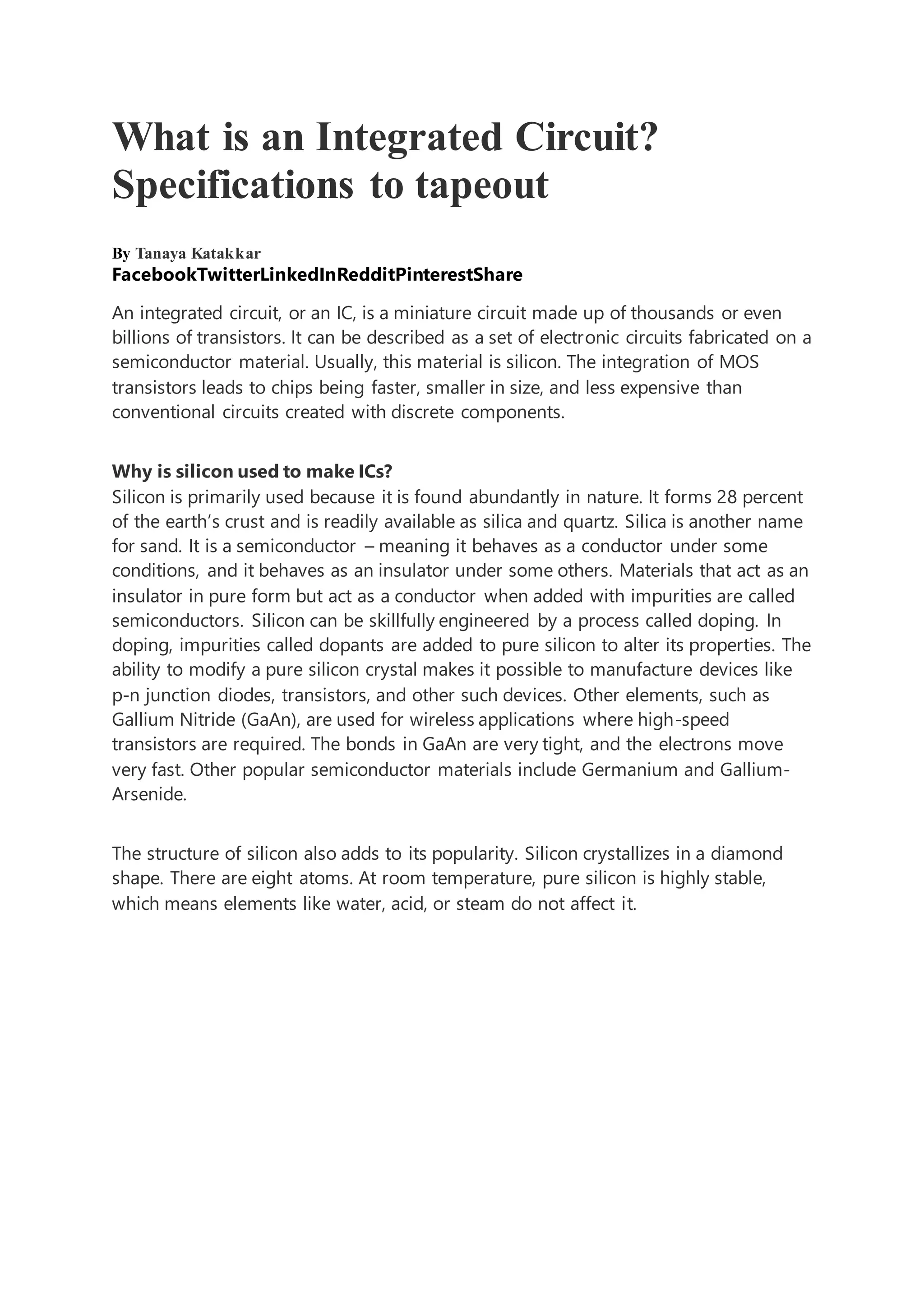
The structure of silicon also adds to its popularity. Silicon crystallizes in a diamond
shape. There are eight atoms. At room temperature, pure silicon is highly stable,
which means elements like water, acid, or steam do not affect it.
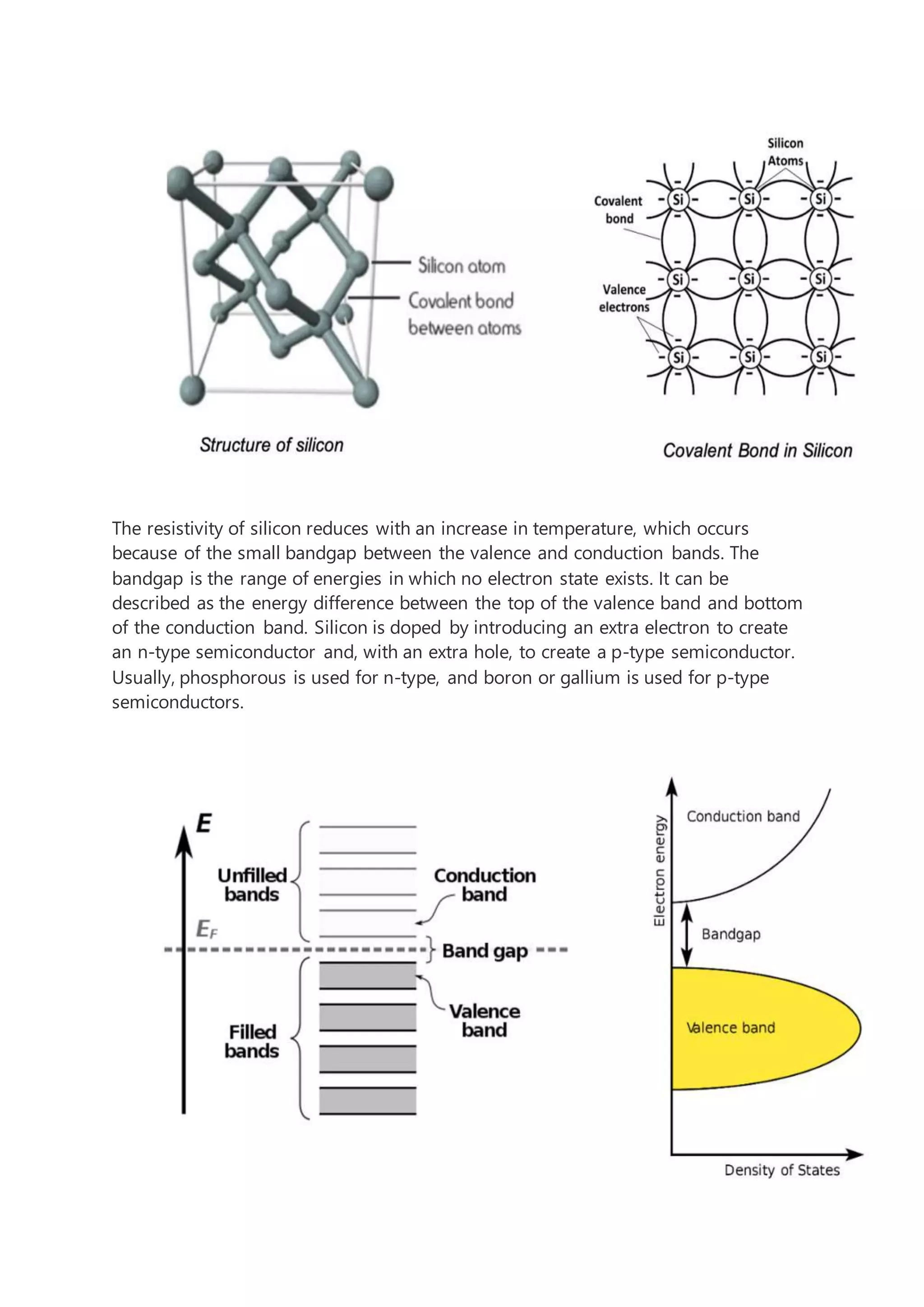
The resistivity of silicon reduces with an increase in temperature, which occurs
because of the small bandgap between the valence and conduction bands. The
bandgap is the range of energies in which no electron state exists. It can be
described as the energy difference between the top of the valence band and bottom
of the conduction band. Silicon is doped by introducing an extra electron to create
an n-type semiconductor and, with an extra hole, to create a p-type semiconductor.
Usually, phosphorous is used for n-type, and boron or gallium is used for p-type
semiconductors.
Semiconductor band structure
Energy bands are formed because of the valence electrons, which are the outermost
electrons of an atom. The bands are involved in electrical conductivity and bonding
and are composed of nearly placed orbitals. Band gaps can be described as energy
ranges that are uncovered by any band. This occurs because energy bands have finite
widths. Silicon has a bandgap of 5.5eV at 302K, where eV stands for electron volts.
IC design flow
IC design can be categorized into digital and analog chip design. Analog chips
include the design and manufacturing of operational amplifiers, oscillators, PLLs, etc.,
whereas digital chips include FPGAs, SoCs, ASICs, etc. Due to the complexity of
modern ICs, which has around a billion transistors on one chip, EDA tools are used
for design, verification, and test. EDA stands for Electronic Design Automation and is
used for the design of electronic systems, including Printed Circuit Boards (PCBs).
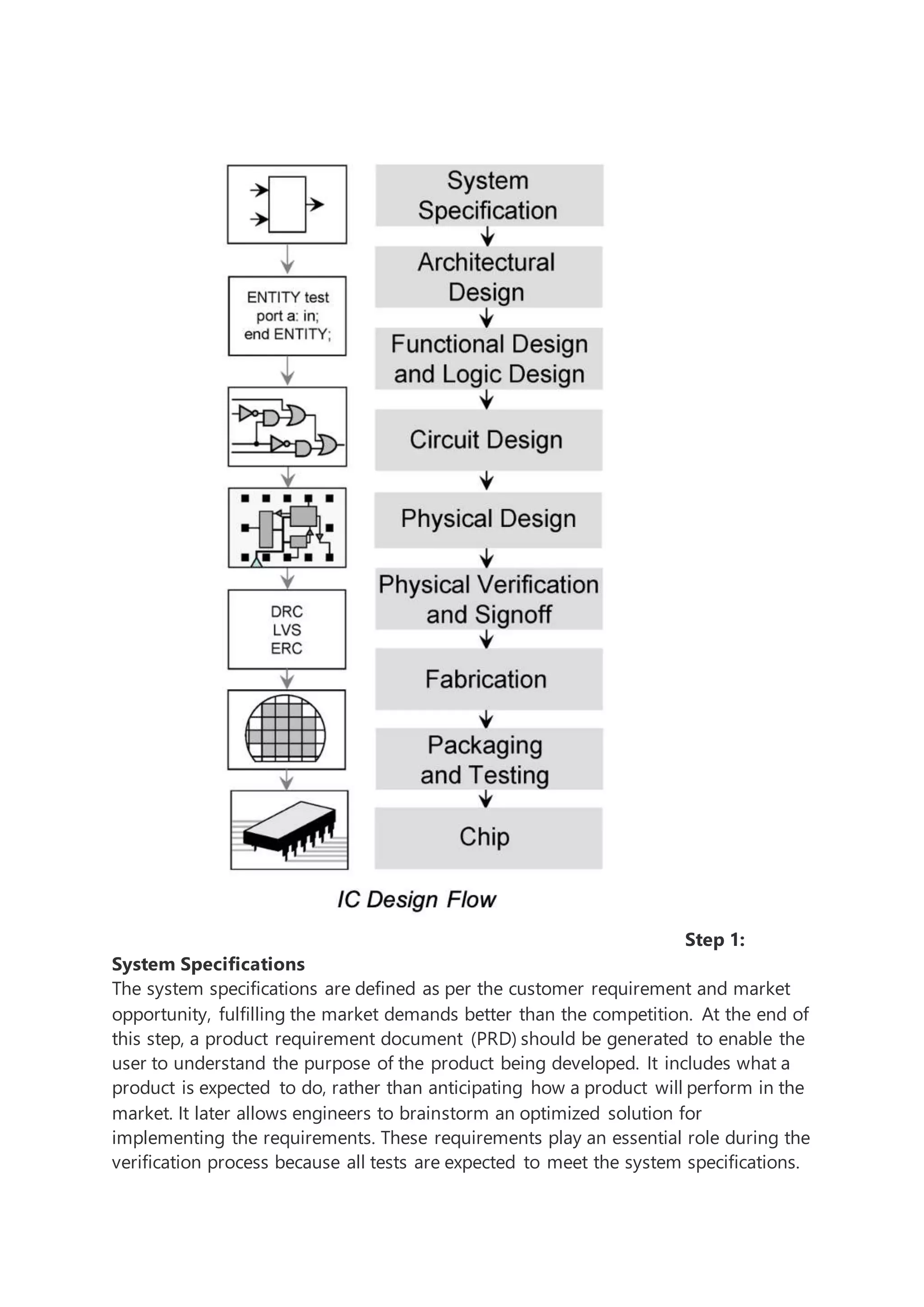
Each step of the design flow has a dedicated EDA tool to perform the required
functionality. EDA tools add flexibility to the chip design. The flowchart below
illustrates the steps involved in manufacturing a chip, from system specifications to
tape-out.
Step 1:
System Specifications
The system specifications are defined as per the customer requirement and market
opportunity, fulfilling the market demands better than the competition. At the end of
this step, a product requirement document (PRD) should be generated to enable the
user to understand the purpose of the product being developed. It includes what a
product is expected to do, rather than anticipating how a product will perform in the
market. It later allows engineers to brainstorm an optimized solution for
implementing the requirements. These requirements play an essential role during the
verification process because all tests are expected to meet the system specifications.
Step 2: Architecture
The design architecture of a product is similar to the block diagram of the product.
The design architect develops the architecture. Microarchitecture functionalities such
as hardware/software interfacing are defined at this stage.
Step 3: Functional design and Logical design
Once the design is agreed upon, the next step is to design the sub-blocks as per the
functionality. RTL (Register Transfer Logic) designers use Hardware Descriptive
Languages like Verilog, SystemVerilog, and VHDL to implement functional and
logical models. This is achieved using digital design components and computer
architecture concepts. The entire model is designed at a higher level of abstraction
using mixed modeling styles.
The verification team works in parallel with the design team to ensure the functional
correctness of design using test vectors for code coverage. Verification of the RTL
code using test benches at this stage is called behavioral simulation. There are two
types of simulation tools, namely functional simulation and timing simulation tools.
Timing simulation is used to verify that the design meets the timing requirements,
and there are no timing delays. A small error at the verification stage can render the
entire chip useless and cost the company millions of dollars for replacement.
Step 4: Circuit Design (Logical Synthesis)
After the RTL code and testbench is generated, the next step is to translate the code
to a gate-level netlist. This is performed using a logic synthesis tool. The netlist
consists of a list of ports, standard cells, their pins, and their interconnections. If any
previously designed macros are present, they are added at this stage.
Once the timing constraints are met, the design proceeds to the Design for
Testability (DFT) stage. DFT techniques improve quality and reduce the cost of testing
while simplifying test, debug, and diagnosis processes. Several scan techniques can
be implemented towards performing DFT.
After DFT, the RTL code and gate-level netlist are compared for equality by reducing
Boolean equations for verification of the netlist. This is called logical equivalency
checking.
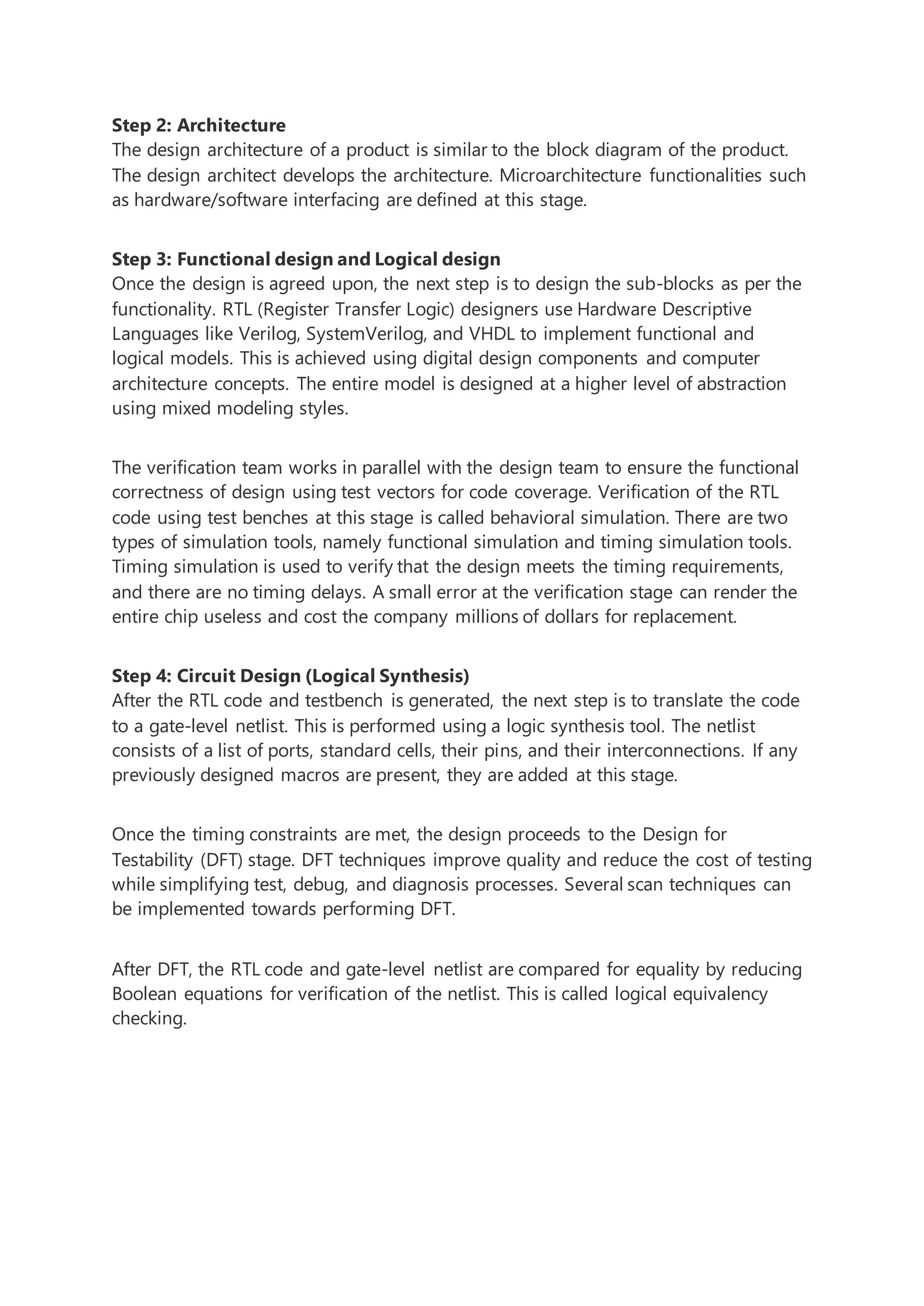
RTL block synthesis process
Step 5: Physical Design
Physical design is the process of representing the RTL in the form of actual geometric
representation. The RTL designed is simply a behavioral model which shows how a
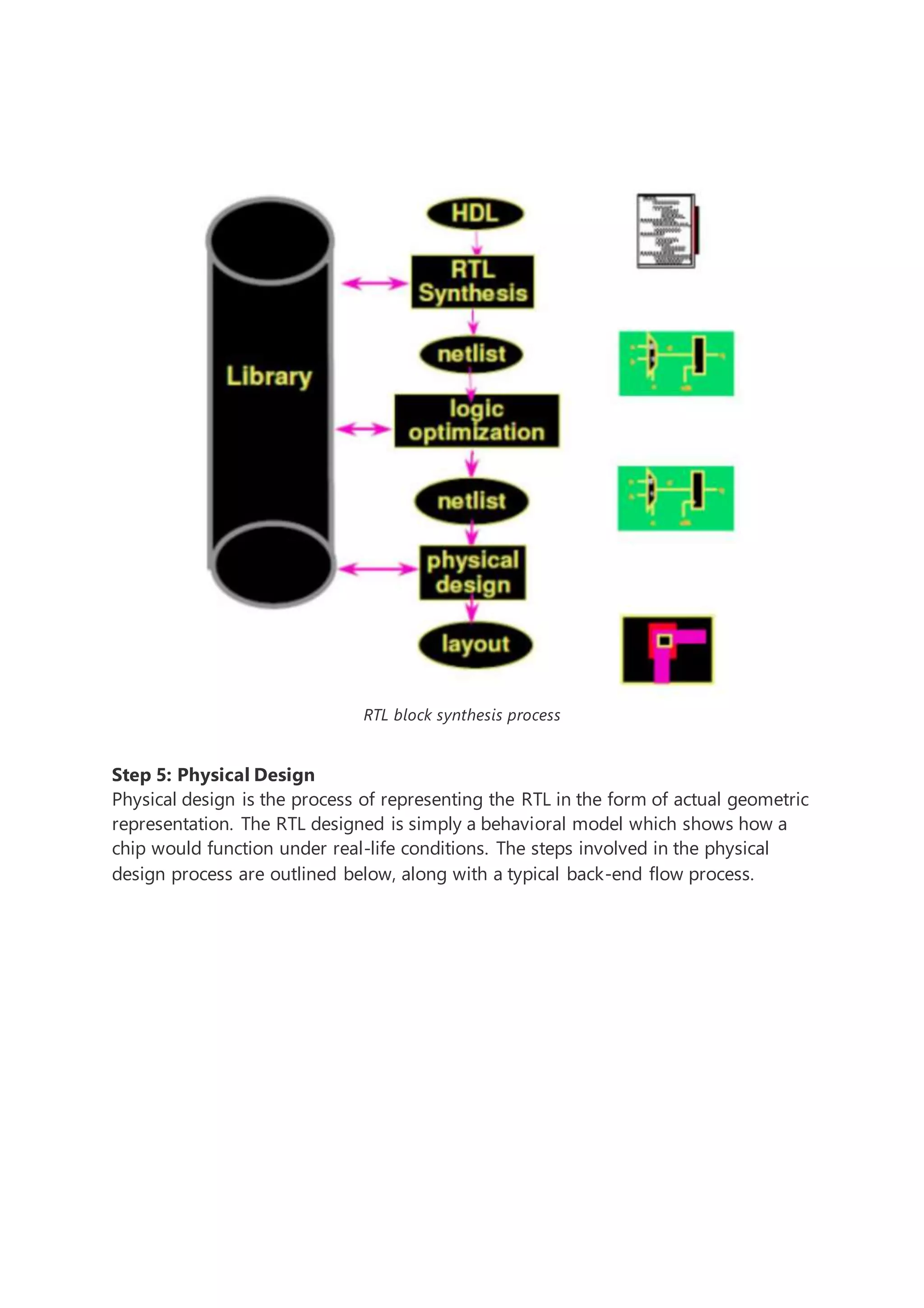
chip would function under real-life conditions. The steps involved in the physical
design process are outlined below, along with a typical back-end flow process.
5.1 Partitioning
The physical design process starts with creating the netlist. The next step is called
partitioning. Partitioning involves dividing the chip into smaller blocks. It can be
described as decomposing a complex system into smaller sub-modules to satisfy the
packaging constraints. It is done to simplify the placement and routing process. The
output at the end of this step will be a set of sub-circuits having the functionality of
the original circuit.
Partitioning helps in minimizing the length of global wires, which in turn decreases
the size of the chip. Partitioning can be done at three levels, namely system-level,
board-level, and chip level.
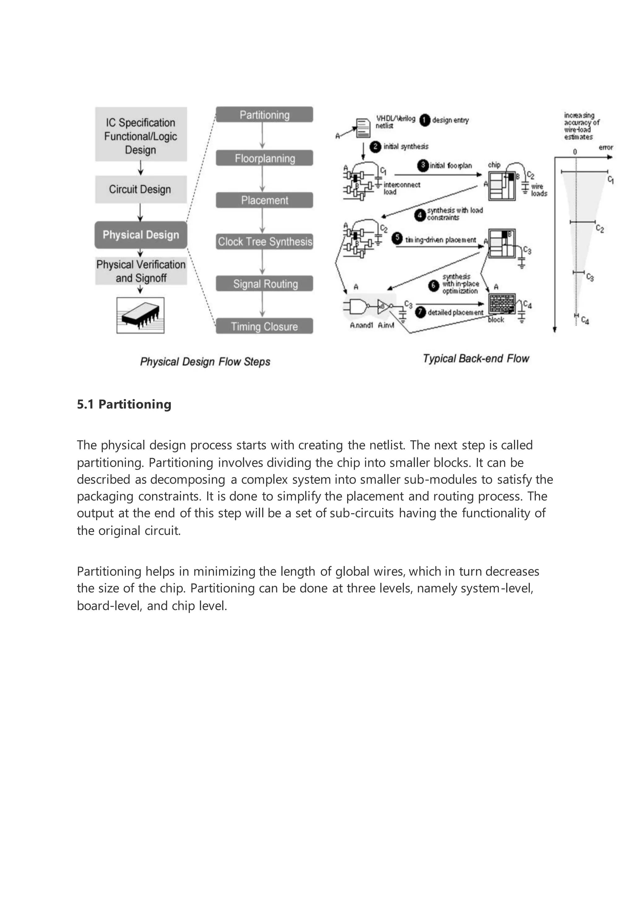
Example of partitioning
Incorrect partitioning can lead to an increase in delay. Partitioning can be done in
two ways: Constructive or iterative and deterministic or probabilistic.
5.2 Floorplanning
As the name suggests, floorplanning is the process of determining structures that
should be placed near each other. Space should be allocated to meet the space
availability, performance expectations. It should not increase the area of the chip, as
this increases the cost. It also takes into account the design IP cores’ placement
needs. IO pins are also placed on the physical chip at this step.
The trade-off between speed and area is the most challenging aspect. This occurs
due to the limited availability of routing resources. An increase in resources used
leads to a decrease in the speed of operation. The data path section is given priority
over non-structured logic. Data path includes modules like adders, subtractors,
counters, and multiplexers.
If a floorplan is not executed correctly, it can lead to congestion in routing and
wastage of die.
5.3 Placement
In placement, gates in the netlist are assigned non-overlapping spaces on the die.
Incorrect placement can affect the performance of the chip and even render it not fit
for manufacturing. Placement uses RC values to calculate delay. All the wire load
modules are removed in this step.
Placement is performed in the following steps:
1. Pre-placement: This step can downsize the cells being placed by collapsing
the high-fanout cells. Fan-out refers to the number of outputs one cell can
have. In short, optimization of the netlist is done at this step.
Insertion of spare cells, adding of special cells, and insertion of decoupling capacitors
is done at this stage.
1. Optimization during placement: The Placement & Routing (PnR) tool is used
for determining an approximate location for all of the cells. The tools optimize
placement as per the timing constraints and congestion.
2. Post Placement optimization before Clock Tree Synthesis: In this step, the
netlist is optimized with ideal clocks. It fixes critical timing violations like setup
time and hold time violations. These violations can lead to a condition called
metastability in which the flip-flop is at an unknown state. If these violations are
not cleared, the chip does not function as desired. Global routing is used for
placement optimization.
3. Post Placement optimization after Clock Tree Synthesis: It attempts to
preserve clock skew. Clock skew occurs in synchronous (clock-based) circuits
wherein the source clock reaches different flops at different times. Clock skew is
classified as positive and negative skew, depending on if the clock is received
before or after the expected time.
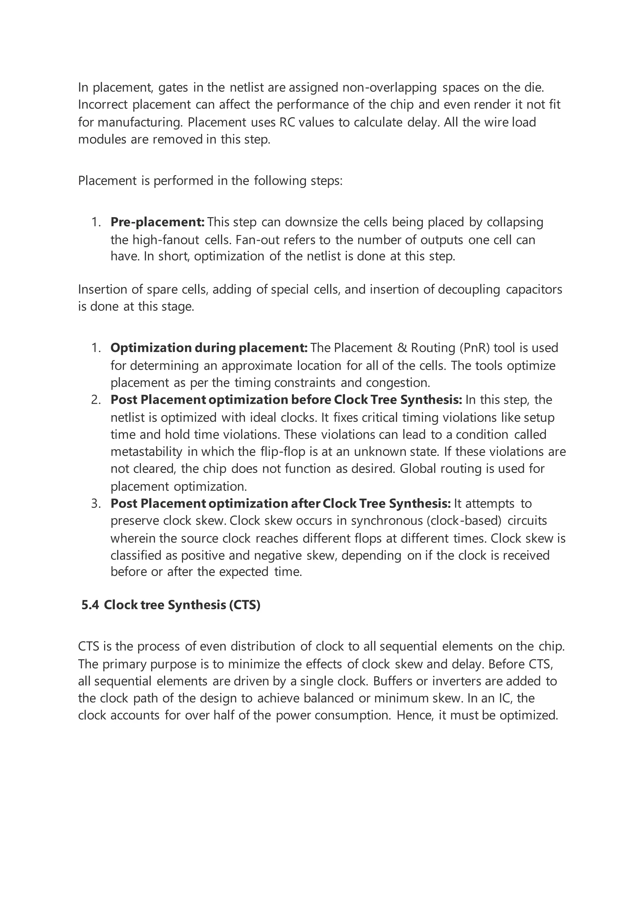
5.4 Clock tree Synthesis (CTS)
CTS is the process of even distribution of clock to all sequential elements on the chip.
The primary purpose is to minimize the effects of clock skew and delay. Before CTS,
all sequential elements are driven by a single clock. Buffers or inverters are added to
the clock path of the design to achieve balanced or minimum skew. In an IC, the
clock accounts for over half of the power consumption. Hence, it must be optimized.
5.5 Signal Routing
In signal routing, interconnections are made for each net by determining a precise
path for every net. It creates wires to connect the properly placed components while
obeying the design rules. Routing is done using EDA tools called routers. Routers aim
to connect every pin to its associated terminals without leaving any pin open or
creating a short. The router needs to ensure that the design meets the timing
constraints. It cannot cross the area of design.
5.6 Timing Closure
Violations related to timing (performance), noise (signal integrity), and design for
manufacturability (yield) are removed.
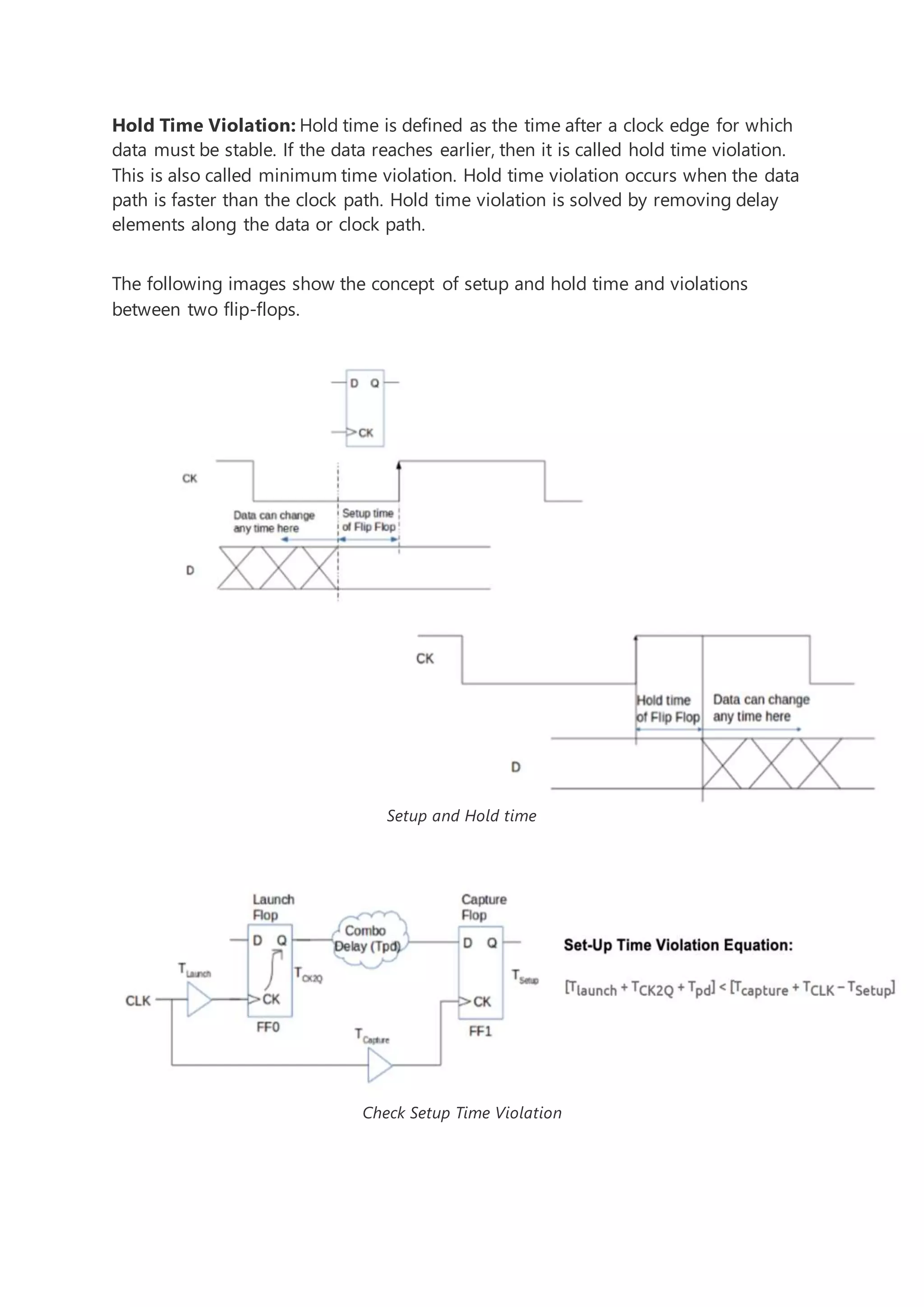
Timing analysis can be done using either Static Timing Analysis (STA) or Dynamic
Timing Analysis. STA checks whether a chip meets the timing constraints without
simulating the design; it does not check the asynchronous part of the design. The
basic timing violations are setup time and hold time violations. STA is performed
using EDA tools built explicitly for this purpose.
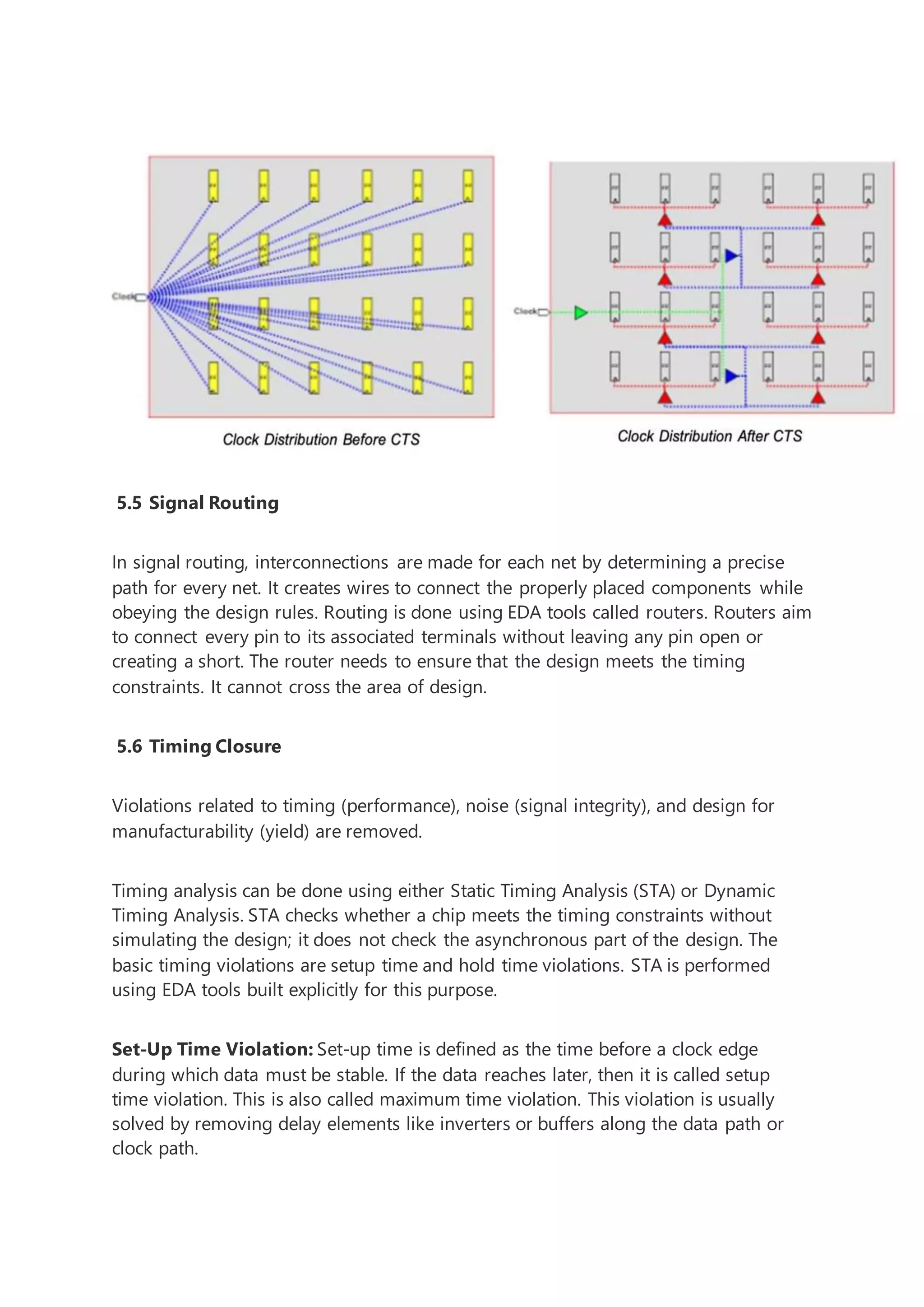
Set-Up Time Violation: Set-up time is defined as the time before a clock edge
during which data must be stable. If the data reaches later, then it is called setup
time violation. This is also called maximum time violation. This violation is usually
solved by removing delay elements like inverters or buffers along the data path or
clock path.
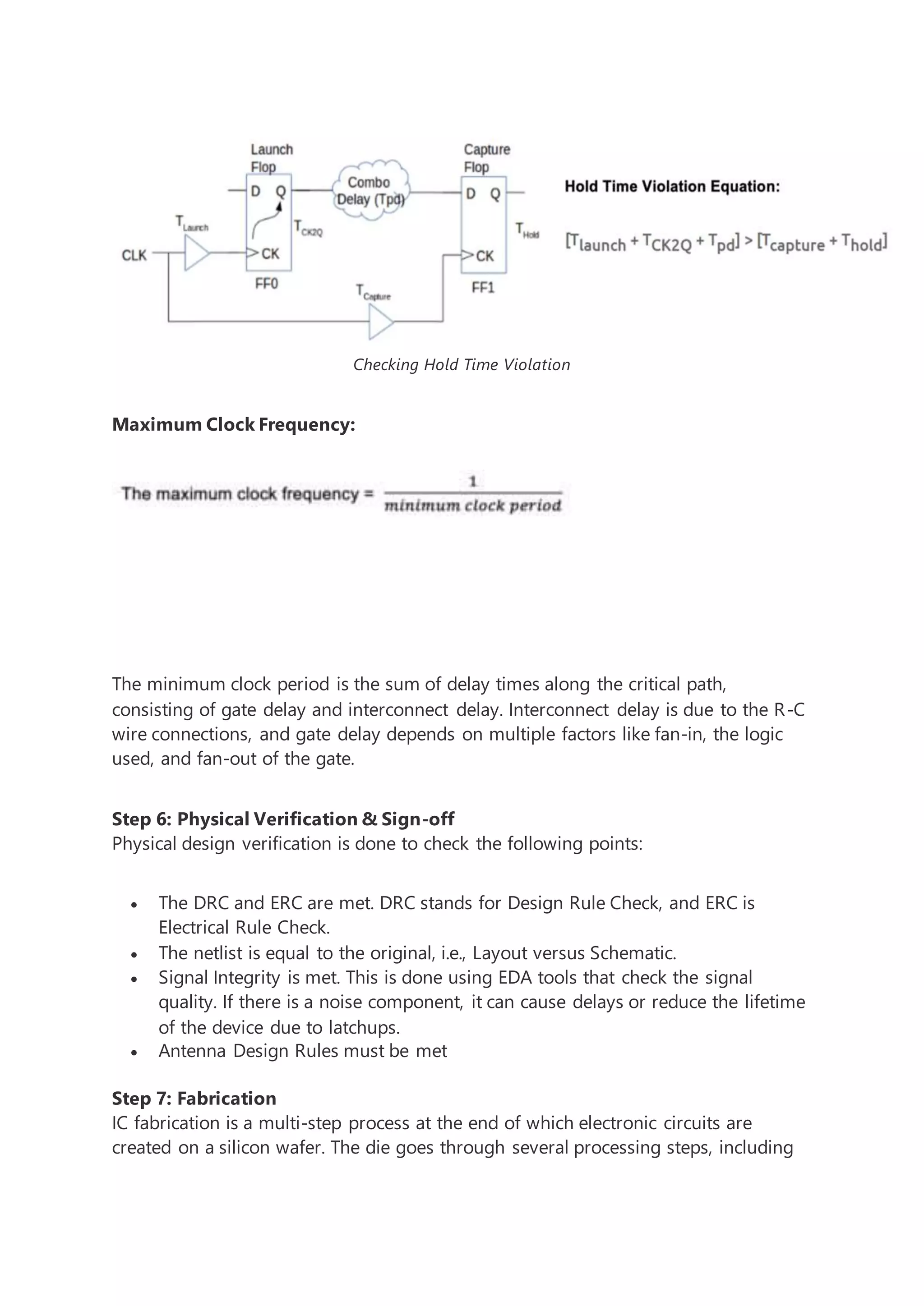
Hold Time Violation: Hold time is defined as the time after a clock edge for which
data must be stable. If the data reaches earlier, then it is called hold time violation.
This is also called minimum time violation. Hold time violation occurs when the data
path is faster than the clock path. Hold time violation is solved by removing delay
elements along the data or clock path.
The following images show the concept of setup and hold time and violations
between two flip-flops.
Setup and Hold time
Check Setup Time Violation
Checking Hold Time Violation
Maximum Clock Frequency:
The minimum clock period is the sum of delay times along the critical path,
consisting of gate delay and interconnect delay. Interconnect delay is due to the R-C
wire connections, and gate delay depends on multiple factors like fan-in, the logic
used, and fan-out of the gate.
Step 6: Physical Verification & Sign-off
Physical design verification is done to check the following points:
 The DRC and ERC are met. DRC stands for Design Rule Check, and ERC is
Electrical Rule Check.
 The netlist is equal to the original, i.e., Layout versus Schematic.
 Signal Integrity is met. This is done using EDA tools that check the signal
quality. If there is a noise component, it can cause delays or reduce the lifetime
of the device due to latchups.
 Antenna Design Rules must be met
Step 7: Fabrication
IC fabrication is a multi-step process at the end of which electronic circuits are
created on a silicon wafer. The die goes through several processing steps, including
photolithography, chemical processing steps like thermal oxidation, and junction
isolation. The entire process can take up to eight weeks.
Step 8: Packaging & Die Test
The package is the block of material that holds the electrical contacts and pins
together. Several IC packages differ as per the customer requirement. The ones most
commonly used today are DIP (Dual-In- Line Package), which may require an IC base.
It is called DIP because there are two rows of pins on either side. Packages such as
ball grid array and thin small-outline packages became popular as the pin count
started exceeding the limit for DIP. The die is prepared as per the package. This is the
final stage of the IC fabrication method.
Step 9: Chip Deployment
At this stage, the chip is wholly verified for functionality. The next step is to create a
datasheet of the IC, outlining the functioning and applications. Each pin is described
in detail along with the basic circuit inside the chip. The chip is deployed and then
analyzed for failures. Failure analysis is the process of gathering data to determine
the causes for failure, if any, which can be fixed in the next iteration of the product.
Before deploying the chip, it goes through bringup. This is the process of testing,
powering, and troubleshooting the first piece of actual hardware. It is subjected to
numerous tests to characterize its performance under various conditions.
Reference: https://www.engineersgarage.com/what-is-an-integrated-circuit-
specifications-to-tapeout/

Full IC Flow.docx

  • 1.
    What is anIntegrated Circuit? Specifications to tapeout By Tanaya Katakkar FacebookTwitterLinkedInRedditPinterestShare An integrated circuit, or an IC, is a miniature circuit made up of thousands or even billions of transistors. It can be described as a set of electronic circuits fabricated on a semiconductor material. Usually, this material is silicon. The integration of MOS transistors leads to chips being faster, smaller in size, and less expensive than conventional circuits created with discrete components. Why is silicon used to make ICs? Silicon is primarily used because it is found abundantly in nature. It forms 28 percent of the earth’s crust and is readily available as silica and quartz. Silica is another name for sand. It is a semiconductor – meaning it behaves as a conductor under some conditions, and it behaves as an insulator under some others. Materials that act as an insulator in pure form but act as a conductor when added with impurities are called semiconductors. Silicon can be skillfully engineered by a process called doping. In doping, impurities called dopants are added to pure silicon to alter its properties. The ability to modify a pure silicon crystal makes it possible to manufacture devices like p-n junction diodes, transistors, and other such devices. Other elements, such as Gallium Nitride (GaAn), are used for wireless applications where high-speed transistors are required. The bonds in GaAn are very tight, and the electrons move very fast. Other popular semiconductor materials include Germanium and Gallium- Arsenide. The structure of silicon also adds to its popularity. Silicon crystallizes in a diamond shape. There are eight atoms. At room temperature, pure silicon is highly stable, which means elements like water, acid, or steam do not affect it.
  • 2.
    The resistivity ofsilicon reduces with an increase in temperature, which occurs because of the small bandgap between the valence and conduction bands. The bandgap is the range of energies in which no electron state exists. It can be described as the energy difference between the top of the valence band and bottom of the conduction band. Silicon is doped by introducing an extra electron to create an n-type semiconductor and, with an extra hole, to create a p-type semiconductor. Usually, phosphorous is used for n-type, and boron or gallium is used for p-type semiconductors.
  • 3.
    Semiconductor band structure Energybands are formed because of the valence electrons, which are the outermost electrons of an atom. The bands are involved in electrical conductivity and bonding and are composed of nearly placed orbitals. Band gaps can be described as energy ranges that are uncovered by any band. This occurs because energy bands have finite widths. Silicon has a bandgap of 5.5eV at 302K, where eV stands for electron volts. IC design flow IC design can be categorized into digital and analog chip design. Analog chips include the design and manufacturing of operational amplifiers, oscillators, PLLs, etc., whereas digital chips include FPGAs, SoCs, ASICs, etc. Due to the complexity of modern ICs, which has around a billion transistors on one chip, EDA tools are used for design, verification, and test. EDA stands for Electronic Design Automation and is used for the design of electronic systems, including Printed Circuit Boards (PCBs). Each step of the design flow has a dedicated EDA tool to perform the required functionality. EDA tools add flexibility to the chip design. The flowchart below illustrates the steps involved in manufacturing a chip, from system specifications to tape-out.
  • 4.
    Step 1: System Specifications Thesystem specifications are defined as per the customer requirement and market opportunity, fulfilling the market demands better than the competition. At the end of this step, a product requirement document (PRD) should be generated to enable the user to understand the purpose of the product being developed. It includes what a product is expected to do, rather than anticipating how a product will perform in the market. It later allows engineers to brainstorm an optimized solution for implementing the requirements. These requirements play an essential role during the verification process because all tests are expected to meet the system specifications.
  • 5.
    Step 2: Architecture Thedesign architecture of a product is similar to the block diagram of the product. The design architect develops the architecture. Microarchitecture functionalities such as hardware/software interfacing are defined at this stage. Step 3: Functional design and Logical design Once the design is agreed upon, the next step is to design the sub-blocks as per the functionality. RTL (Register Transfer Logic) designers use Hardware Descriptive Languages like Verilog, SystemVerilog, and VHDL to implement functional and logical models. This is achieved using digital design components and computer architecture concepts. The entire model is designed at a higher level of abstraction using mixed modeling styles. The verification team works in parallel with the design team to ensure the functional correctness of design using test vectors for code coverage. Verification of the RTL code using test benches at this stage is called behavioral simulation. There are two types of simulation tools, namely functional simulation and timing simulation tools. Timing simulation is used to verify that the design meets the timing requirements, and there are no timing delays. A small error at the verification stage can render the entire chip useless and cost the company millions of dollars for replacement. Step 4: Circuit Design (Logical Synthesis) After the RTL code and testbench is generated, the next step is to translate the code to a gate-level netlist. This is performed using a logic synthesis tool. The netlist consists of a list of ports, standard cells, their pins, and their interconnections. If any previously designed macros are present, they are added at this stage. Once the timing constraints are met, the design proceeds to the Design for Testability (DFT) stage. DFT techniques improve quality and reduce the cost of testing while simplifying test, debug, and diagnosis processes. Several scan techniques can be implemented towards performing DFT. After DFT, the RTL code and gate-level netlist are compared for equality by reducing Boolean equations for verification of the netlist. This is called logical equivalency checking.
  • 6.
    RTL block synthesisprocess Step 5: Physical Design Physical design is the process of representing the RTL in the form of actual geometric representation. The RTL designed is simply a behavioral model which shows how a chip would function under real-life conditions. The steps involved in the physical design process are outlined below, along with a typical back-end flow process.
  • 7.
    5.1 Partitioning The physicaldesign process starts with creating the netlist. The next step is called partitioning. Partitioning involves dividing the chip into smaller blocks. It can be described as decomposing a complex system into smaller sub-modules to satisfy the packaging constraints. It is done to simplify the placement and routing process. The output at the end of this step will be a set of sub-circuits having the functionality of the original circuit. Partitioning helps in minimizing the length of global wires, which in turn decreases the size of the chip. Partitioning can be done at three levels, namely system-level, board-level, and chip level.
  • 8.
    Example of partitioning Incorrectpartitioning can lead to an increase in delay. Partitioning can be done in two ways: Constructive or iterative and deterministic or probabilistic. 5.2 Floorplanning As the name suggests, floorplanning is the process of determining structures that should be placed near each other. Space should be allocated to meet the space availability, performance expectations. It should not increase the area of the chip, as this increases the cost. It also takes into account the design IP cores’ placement needs. IO pins are also placed on the physical chip at this step. The trade-off between speed and area is the most challenging aspect. This occurs due to the limited availability of routing resources. An increase in resources used leads to a decrease in the speed of operation. The data path section is given priority over non-structured logic. Data path includes modules like adders, subtractors, counters, and multiplexers. If a floorplan is not executed correctly, it can lead to congestion in routing and wastage of die. 5.3 Placement
  • 9.
    In placement, gatesin the netlist are assigned non-overlapping spaces on the die. Incorrect placement can affect the performance of the chip and even render it not fit for manufacturing. Placement uses RC values to calculate delay. All the wire load modules are removed in this step. Placement is performed in the following steps: 1. Pre-placement: This step can downsize the cells being placed by collapsing the high-fanout cells. Fan-out refers to the number of outputs one cell can have. In short, optimization of the netlist is done at this step. Insertion of spare cells, adding of special cells, and insertion of decoupling capacitors is done at this stage. 1. Optimization during placement: The Placement & Routing (PnR) tool is used for determining an approximate location for all of the cells. The tools optimize placement as per the timing constraints and congestion. 2. Post Placement optimization before Clock Tree Synthesis: In this step, the netlist is optimized with ideal clocks. It fixes critical timing violations like setup time and hold time violations. These violations can lead to a condition called metastability in which the flip-flop is at an unknown state. If these violations are not cleared, the chip does not function as desired. Global routing is used for placement optimization. 3. Post Placement optimization after Clock Tree Synthesis: It attempts to preserve clock skew. Clock skew occurs in synchronous (clock-based) circuits wherein the source clock reaches different flops at different times. Clock skew is classified as positive and negative skew, depending on if the clock is received before or after the expected time. 5.4 Clock tree Synthesis (CTS) CTS is the process of even distribution of clock to all sequential elements on the chip. The primary purpose is to minimize the effects of clock skew and delay. Before CTS, all sequential elements are driven by a single clock. Buffers or inverters are added to the clock path of the design to achieve balanced or minimum skew. In an IC, the clock accounts for over half of the power consumption. Hence, it must be optimized.
  • 10.
    5.5 Signal Routing Insignal routing, interconnections are made for each net by determining a precise path for every net. It creates wires to connect the properly placed components while obeying the design rules. Routing is done using EDA tools called routers. Routers aim to connect every pin to its associated terminals without leaving any pin open or creating a short. The router needs to ensure that the design meets the timing constraints. It cannot cross the area of design. 5.6 Timing Closure Violations related to timing (performance), noise (signal integrity), and design for manufacturability (yield) are removed. Timing analysis can be done using either Static Timing Analysis (STA) or Dynamic Timing Analysis. STA checks whether a chip meets the timing constraints without simulating the design; it does not check the asynchronous part of the design. The basic timing violations are setup time and hold time violations. STA is performed using EDA tools built explicitly for this purpose. Set-Up Time Violation: Set-up time is defined as the time before a clock edge during which data must be stable. If the data reaches later, then it is called setup time violation. This is also called maximum time violation. This violation is usually solved by removing delay elements like inverters or buffers along the data path or clock path.
  • 11.
    Hold Time Violation:Hold time is defined as the time after a clock edge for which data must be stable. If the data reaches earlier, then it is called hold time violation. This is also called minimum time violation. Hold time violation occurs when the data path is faster than the clock path. Hold time violation is solved by removing delay elements along the data or clock path. The following images show the concept of setup and hold time and violations between two flip-flops. Setup and Hold time Check Setup Time Violation
  • 12.
    Checking Hold TimeViolation Maximum Clock Frequency: The minimum clock period is the sum of delay times along the critical path, consisting of gate delay and interconnect delay. Interconnect delay is due to the R-C wire connections, and gate delay depends on multiple factors like fan-in, the logic used, and fan-out of the gate. Step 6: Physical Verification & Sign-off Physical design verification is done to check the following points:  The DRC and ERC are met. DRC stands for Design Rule Check, and ERC is Electrical Rule Check.  The netlist is equal to the original, i.e., Layout versus Schematic.  Signal Integrity is met. This is done using EDA tools that check the signal quality. If there is a noise component, it can cause delays or reduce the lifetime of the device due to latchups.  Antenna Design Rules must be met Step 7: Fabrication IC fabrication is a multi-step process at the end of which electronic circuits are created on a silicon wafer. The die goes through several processing steps, including
  • 13.
    photolithography, chemical processingsteps like thermal oxidation, and junction isolation. The entire process can take up to eight weeks. Step 8: Packaging & Die Test The package is the block of material that holds the electrical contacts and pins together. Several IC packages differ as per the customer requirement. The ones most commonly used today are DIP (Dual-In- Line Package), which may require an IC base. It is called DIP because there are two rows of pins on either side. Packages such as ball grid array and thin small-outline packages became popular as the pin count started exceeding the limit for DIP. The die is prepared as per the package. This is the final stage of the IC fabrication method. Step 9: Chip Deployment At this stage, the chip is wholly verified for functionality. The next step is to create a datasheet of the IC, outlining the functioning and applications. Each pin is described in detail along with the basic circuit inside the chip. The chip is deployed and then analyzed for failures. Failure analysis is the process of gathering data to determine the causes for failure, if any, which can be fixed in the next iteration of the product. Before deploying the chip, it goes through bringup. This is the process of testing, powering, and troubleshooting the first piece of actual hardware. It is subjected to numerous tests to characterize its performance under various conditions. Reference: https://www.engineersgarage.com/what-is-an-integrated-circuit- specifications-to-tapeout/