SlideShare a Scribd company logo
PACKAGING
OF VLSI
DEVICES
Package Types,
Packaging Design
Consideration
ASHUTOSH SINGH
B Tech 4th year (ECE)
Hindustan Institute of
Technology
0821331024
TABLE OF CONTENTS
1. INTRODUCTION
2. PACKAGE DESIGN CONSIDERATIONS
Number of terminals
Electrical design considerations
Thermal design consideration
Reliability
Testability
3. PACKAGE TYPES
Through hole packages
Surface mounted packages
Flip chip packages
Chip size packages
Multi chip modules
3-D VLSI packaging
INTRODUCTION
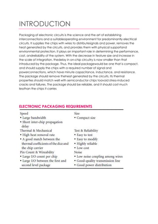
Packaging of electronic circuits is the science and the art of establishing
interconnections and a suitableoperating environment for predominantly electrical
circuits. It supplies the chips with wires to distributesignals and power, removes the
heat generated by the circuits, and provides them with physical supportand
environmental protection. It plays an important role in determining the performance,
cost, andreliability of the system. With the decrease in feature size and increase in
the scale of integration, thedelay in on-chip circuitry is now smaller than that
introduced by the package. Thus, the ideal packagewould be one that is compact,
and should supply the chips with a required number of signal and
powerconnections, which have minute capacitance, inductance, and resistance.
The package should remove theheat generated by the circuits. Its thermal
properties should match well with semiconductor chips toavoid stress-induced
cracks and failures. The package should be reliable, and it should cost much
lessthan the chips it carries
ELECTRONIC PACKAGING REQUIREMENTS
PACKAGE DESIGN
CONSIDERATIONS: PACKAGE
PARAMETERS
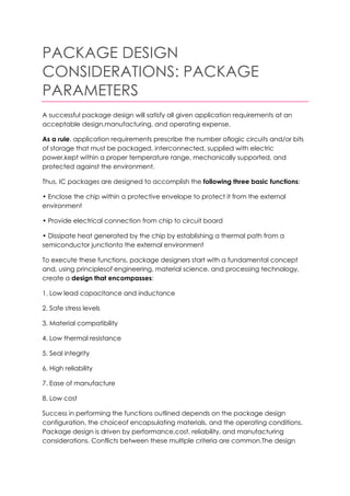
A successful package design will satisfy all given application requirements at an
acceptable design,manufacturing, and operating expense.
As a rule, application requirements prescribe the number oflogic circuits and/or bits
of storage that must be packaged, interconnected, supplied with electric
power,kept within a proper temperature range, mechanically supported, and
protected against the environment.
Thus, IC packages are designed to accomplish the following three basic functions:
• Enclose the chip within a protective envelope to protect it from the external
environment
• Provide electrical connection from chip to circuit board
• Dissipate heat generated by the chip by establishing a thermal path from a
semiconductor junctionto the external environment
To execute these functions, package designers start with a fundamental concept
and, using principlesof engineering, material science, and processing technology,
create a design that encompasses:
1. Low lead capacitance and inductance
2. Safe stress levels
3. Material compatibility
4. Low thermal resistance
5. Seal integrity
6. High reliability
7. Ease of manufacture
8. Low cost
Success in performing the functions outlined depends on the package design
configuration, the choiceof encapsulating materials, and the operating conditions.
Package design is driven by performance,cost, reliability, and manufacturing
considerations. Conflicts between these multiple criteria are common.The design
process involves many trade-off analyses and the optimization of conflicting
requirements.
While designing the package for an application, the following parameters are
considered:
Number of Terminals
The total number of terminals at packaging interfaces is a major cost factor. Signal
interconnections andterminals constitute the majority of conducting elements. Other
conductors supply power and provideground or other reference voltages.The
number of terminals supporting a group of circuits is strongly dependent on the
function of thisgroup. The smallest pin-out can be obtained with memory ICs
because the stream of data can be limitedto a single bit. Exactly the opposite is the
case with groups of logic circuits which result from a randompartitioning of a
computer. The pin-out requirement is one of the key driving parameters for all levels
ofpackaging: chips, chip carriers, cards, modules, cables, and cable connectors.
Electrical Design Considerations
Electrical performance at the IC package level is of great importance for
microwave designs and hasgained considerable attention recently for silicon digital
devices due to ever-increasing speed of today’scircuits and their potentially
reduced noise margins.As a signal propagates through the package, it isdegraded
due to reflections and line resistance. Controlling the resistance and the inductance
associatedwith the power and ground distribution paths to combat ground bounce
and the simultaneous switchingnoise has now become essential. Controlling the
impedance environment of the signal distribution pathin the package to mitigate
the reflection-related noise is becoming important. Reflections, in addition,cause an
increase in the transition time, and may split the signal into two or more pulses with
the potentialof causing erroneous switching in the subsequent circuit and thus
malfunction of the system. Controllingthe capacitive coupling between signal traces
in the signal distribution path to reduce crosstalk is gainingimportance. Increased
speed of the devices demands that package bandwidth be increased to
reduceundue distortion of the signal. All these criteria are related through geometric
variables, such as conductorcross-section and length, dielectric thickness, and the
dielectric constant of the packaging body. Theseproblems are usually handled with
transmission line theory.
Thermal Design Considerations
The thermal design objective is to keep the operating junction temperature of a
silicon chip low enoughto prevent triggering the temperature-activated failure
mechanisms. Thus, the package should provide agood medium for heat transfer
from junction to the ambient/heat sink. It is generally recommended tokeep the
junction temperature below 150°C to ensure proper electrical performance and to
contain thepropensity to fail.Thermal expansion caused by heating up the
packaging structure is not uniform — it varies inaccordance with the temperature
gradient at any point in time and with the mismatches in the thermalcoefficient of
expansion. Mechanical stresses result from these differences and are one of the
contributorsto the finite lifetime and the failure rate of any packaging structure.In a
simplistic heat transfer model of a packaged chip, the heat is transferred from the
chip to thesurface of the package by conduction and from the package surface to
the ambient by convection andradiation.Typically, the temperature difference
between the case and ambient is small, and henceradiation can be neglected. This
model also neglects conduction heat transfer out of the package terminals,which
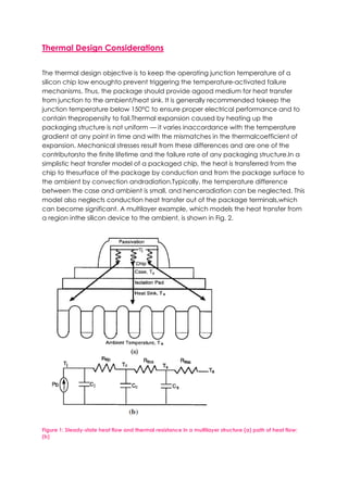
can become significant. A multilayer example, which models the heat transfer from
a region inthe silicon device to the ambient, is shown in Fig. 2.
Figure 1: Steady-state heat flow and thermal resistance in a multilayer structure (a) path of heat flow;
(b)
The total thermal resistance from the junctionto the ambient is given by:
The resulting junction temperature, assuming a power dissipation of Pd, is
in analogy with electric circuits. If there are parallel paths for heat flow, the thermal
resistances arecombined in exactly the same manner as electrical resistors in
parallel.
Rθcs, the conductive thermal resistance, is mainly a function of package materials
and geometry. Withthe higher power requirements, one must consider the
temperature dependence of materials selected indesign.
Tj depends on package geometry, package orientation in the application, and the
conditions ofthe ambient in the operating environment. The heat sink is responsible
for getting rid of the heat of theenvironment by convection and radiation. Because
of all the many heat transfer modes occurring in afinned heat sink, the accurate
way to obtain the exact thermal resistance of the heat sink would be tomeasure it.
However, most heat sink manufacturers today provide information about their
extrusionsconcerning the thermal resistance per unit length.
Reliability
The package should have good thermo-mechanical performance for better
reliability. A variety of materialsof widely differing coefficients of thermal expansion
(CTEs) are joined to create interfaces. These interfacesare subject to relatively high
process temperatures and undergo many temperature cycles in theiruseful life as
the device is powered on and off. As a result, residual stresses are created in the
interfaces.These stresses cause reliability problems in the packages.
Testability
Implicit in reliability considerations is the assumption of a flawless product function
after its initialassembly — a zero defect manufacturing. Although feasible in
principle, it is rarely practiced because ofthe high costs and possible loss of
competitive edge due to conservative dimensions, tolerances, materials,and
process choices. So, several tests are employed to assess the reliability of the
packages.
PACKAGE TYPES
IC packages have been developed over time to meet the requirements of high
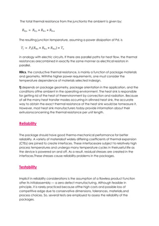
speed and density. Thehistory of IC package development has been the continuous
battle to miniaturize.Figure 3 illustratesthe size and weight reduction of IC packages
over time.
Figure 2: Packaging trends
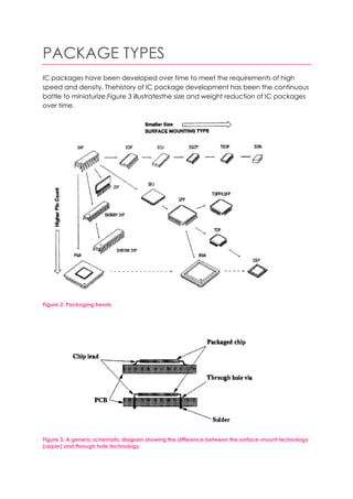
Figure 3: A generic schematic diagram showing the difference between the surface-mount technology
(upper) and through hole technology
Several packages can be classified as follows:
Through Hole Packages
Through-the-board hole mounting technology uses precision holes drilled through
the board and platedwith copper. This copper plating forms the connections
between separate layers. These layers consist ofthin copper sheets stacked together
and insulated by epoxy fiber-glass. There are no dedicated via structuresto make
connections between wiring levels; through holes serve that purpose. Through holes
form asturdy support for the chip carrier and resist thermal and mechanical stresses
caused by the variationsin the expansions of components at raised temperatures.
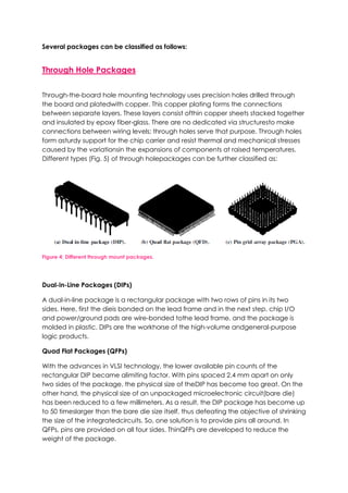
Different types (Fig. 5) of through holepackages can be further classified as:
Figure 4: Different through mount packages.
Dual-in-Line Packages (DIPs)
A dual-in-line package is a rectangular package with two rows of pins in its two
sides. Here, first the dieis bonded on the lead frame and in the next step, chip I/O
and power/ground pads are wire-bonded tothe lead frame, and the package is
molded in plastic. DIPs are the workhorse of the high-volume andgeneral-purpose
logic products.
Quad Flat Packages (QFPs)
With the advances in VLSI technology, the lower available pin counts of the
rectangular DIP became alimiting factor. With pins spaced 2.4 mm apart on only
two sides of the package, the physical size of theDIP has become too great. On the
other hand, the physical size of an unpackaged microelectronic circuit(bare die)
has been reduced to a few millimeters. As a result, the DIP package has become up
to 50 timeslarger than the bare die size itself, thus defeating the objective of shrinking
the size of the integratedcircuits. So, one solution is to provide pins all around. In
QFPs, pins are provided on all four sides. ThinQFPs are developed to reduce the
weight of the package.
Pin Grid Arrays (PGA)
A pin grid array has leads on its entire bottom surface rather than only at its
periphery. This way it can offera much larger pin count. It has cavity-up and cavity-
down versions. In a cavity-down version, a die is mountedon the same side as the
pins facing toward the PC board, and a heat sink can be mounted on its backside
toimprove the heat flow. When the cavity and the pins are on the same side, the
total number of pins is reducedbecause the area occupied by the cavity is not
available for brazed pins. The mounting and wire bonding ofthe dice are also more
difficult because of the existence of the pins next to the cavity. High pin count
andlarger power dissipation capability of PGAs make them attractive for different
types of packaging.
Surface-Mounted Packages
Surface mounting solves many of the shortcomings of through-the-board mounting.
In this technology,a chip carrier is soldered to the pads on the surface of a board
without requiring any through holes. Thesmaller component sizes, lack of through
holes, and the possibility of mounting chips on both sides ofthe PC board improve
the board density. This reduces package parasitic capacitances and
inductancesassociated with the package pins and board wiring. Various types of
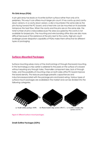
surface-mount packages are availableon the market and can be divided into the
following categories.
Figure 5: Different surface-mount packages.
Small-Outline Packages (SOPs)
The small-outline package has gull-wing shaped leads. It requires less pin spacing
than through-holemountedDIPs and PGAs. SOP packages usually have small lead
counts and are used for discrete, analog,and SSI/MSI logic parts.
Plastic-leaded Chip Carriers (PLCCs)
Plastic-leaded chip carriers, such as gull-wing and J-leaded chip carriers, offer higher
pin counts thanSOP. J-leaded chip carriers pack denser and are more suitable for
automation than gull-wing leadedcarriers because their leads do not extend
beyond the package.
Leadless Ceramic Chip Carriers (LCCCs)
Leadless ceramic chip carriers take advantage of multilayer ceramic technology.
The conductors are leftexposed around the package periphery to provide contacts
for surface mounting. Dice in leadless chipcarriers are mounted in cavity-down
position, and the back side of the chip faces away from the board,providing a good
heat removal path. The ceramic substrate also has a high thermal conductivity.
LCCCsare hermetically sealed.
Flip-Chip Packages
The length of the electrical connections between the chip and the substrate can be
minimized by placingsolder bumps on the dice, flipping the chips over, aligning
them with the contacts pads on the substrate,and reflowing the solder balls in a
furnace to establish the bonding between the chips and the package.
This method provides electrical connections with minute parasitic inductance and
capacitance. In addition,contact pads are distributed over the entire chip surface.
This saves silicon area, increases themaximum I/O and power/ground terminals
available with a given die size, and provides more efficientlyrouted signal and
power/ground interconnections on the chips.
Figure 6: Flip chip packaging and its interconnections.
Chip Size Packages (CSPs)
To combine the advantages of both packaged chip and bare chip in one solution,
a variety of CSPs havebeen developed. CSPs can be divided into two categories:
the fan-in type and the fan-out type.
Fan-in type CSPs are suitable for memory applications that have relatively low pin
counts. This typeis further divided into two types, depending on the location of
bonding pads on the chip surface; theseare the center pad type and the peripheral
pad type. This type of CSP keeps all the solder bumps withinthe chip area by
arranging bumps in area array format on the chip surface.
The fan-out CSPs are used mainly for logic applications: because of the die size to
pin count ratio,the solder bumps cannot be designed within the chip area.
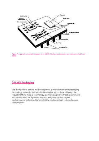
Multi-Chip Modules (MCMs)
In a multi-chip module, several chips are supported on a single package. Most multi-
chip packages aremade of ceramic. By eliminating one level of packaging, the
inductance and capacitance of the electricalconnections among the dice are
reduced. Usually, the dice are mounted on a multilayer ceramic substratevia solder
bumps, and the ceramic substrate offers a dense interconnection network. There
are several advantages of multi-chip modules over single-chip carriers. The multi-
chip moduleminimizes the chip-to-chip spacing and reduces the inductive and
capacitive discontinuities between thechips mounted on the substrate by replacing
the die-bump-interconnect-bump-die path. In addition,narrower and shorter wires
on the ceramic substrate have much less capacitance and inductance thanthe PC
board interconnections.
Figure 7: A generic schematic diagram of an MCM, showing how bare dice are interconnected to an
MCM
3-D VLSI Packaging
The driving forces behind the development of three-dimensional packaging
technology are similar to themulti-chip module technology, although the
requirements for the 3-D technology are more aggressive.These requirements
include the need for significant size and weight reductions, higher
performance,small delay, higher reliability, and potentially reduced power
consumption.

More Related Content

Similar to types of packages.pdf

A 2D MODELLING OF THERMAL HEAT SINK FOR IMPATT AT HIGH POWER MMW FREQUENCY
A 2D MODELLING OF THERMAL HEAT SINK FOR IMPATT AT HIGH POWER MMW FREQUENCYA 2D MODELLING OF THERMAL HEAT SINK FOR IMPATT AT HIGH POWER MMW FREQUENCY
A 2D MODELLING OF THERMAL HEAT SINK FOR IMPATT AT HIGH POWER MMW FREQUENCY
cscpconf
 
A Novel Methodlogy For Thermal Ananalysis & 3-Dimensional Memory Integration
A Novel Methodlogy For Thermal Ananalysis & 3-Dimensional Memory IntegrationA Novel Methodlogy For Thermal Ananalysis & 3-Dimensional Memory Integration
A Novel Methodlogy For Thermal Ananalysis & 3-Dimensional Memory Integration
ijait
 
A NOVEL METHODLOGY FOR THERMAL ANANALYSIS & 3-DIMENSIONAL MEMORY INTEGRATION
A NOVEL METHODLOGY FOR THERMAL ANANALYSIS & 3-DIMENSIONAL MEMORY INTEGRATION A NOVEL METHODLOGY FOR THERMAL ANANALYSIS & 3-DIMENSIONAL MEMORY INTEGRATION
A NOVEL METHODLOGY FOR THERMAL ANANALYSIS & 3-DIMENSIONAL MEMORY INTEGRATION
ijait
 
Active cooling technique using peltier element for efficient heat mitigation ...
Active cooling technique using peltier element for efficient heat mitigation ...Active cooling technique using peltier element for efficient heat mitigation ...
Active cooling technique using peltier element for efficient heat mitigation ...
IAEME Publication
 
Mems capacitor
Mems capacitorMems capacitor
Mems capacitor
Engr Syed Absar Kazmi
 
IEEE Research Article - Polymeric Packaging of High Power Semi-Conductors
IEEE Research Article - Polymeric Packaging of High Power Semi-ConductorsIEEE Research Article - Polymeric Packaging of High Power Semi-Conductors
IEEE Research Article - Polymeric Packaging of High Power Semi-Conductors
Kashif Kamran Ahmad
 
Analysis of polymer polymethyl metha-acralyte and single-wall cnt composites
Analysis of polymer polymethyl metha-acralyte and single-wall cnt compositesAnalysis of polymer polymethyl metha-acralyte and single-wall cnt composites
Analysis of polymer polymethyl metha-acralyte and single-wall cnt composites
IAEME Publication
 
IRJET- Development of MGO-EPOXY Composites with Enhanced Thermal Conductivity
IRJET- Development of MGO-EPOXY Composites with Enhanced Thermal ConductivityIRJET- Development of MGO-EPOXY Composites with Enhanced Thermal Conductivity
IRJET- Development of MGO-EPOXY Composites with Enhanced Thermal Conductivity
IRJET Journal
 
Package fabrication technolog ynew
Package fabrication technolog ynewPackage fabrication technolog ynew
Package fabrication technolog ynew
prashant singh
 
Thermal monitoring of cable circuits and grid operators' use of dynamic ratin...
Thermal monitoring of cable circuits and grid operators' use of dynamic ratin...Thermal monitoring of cable circuits and grid operators' use of dynamic ratin...
Thermal monitoring of cable circuits and grid operators' use of dynamic ratin...
Power System Operation
 
If2414451450
If2414451450If2414451450
If2414451450
IJERA Editor
 
Undergrounding high voltage_electricity_transmission_lines_the_technical_issu...
Undergrounding high voltage_electricity_transmission_lines_the_technical_issu...Undergrounding high voltage_electricity_transmission_lines_the_technical_issu...
Undergrounding high voltage_electricity_transmission_lines_the_technical_issu...
Ivan Rojas Soliz
 
Vishwakarma-MicroEng2015
Vishwakarma-MicroEng2015Vishwakarma-MicroEng2015
Vishwakarma-MicroEng2015
Chirag Waghela
 
Electrical signal interference minimization using appropriate core material f...
Electrical signal interference minimization using appropriate core material f...Electrical signal interference minimization using appropriate core material f...
Electrical signal interference minimization using appropriate core material f...
IJECEIAES
 
Effects of backfilling on cable ampacity analyzed with the finite element method
Effects of backfilling on cable ampacity analyzed with the finite element methodEffects of backfilling on cable ampacity analyzed with the finite element method
Effects of backfilling on cable ampacity analyzed with the finite element method
thinknice
 
Probe Card Manufacturing Paving the Way for Semiconductor Testing Excellence
Probe Card Manufacturing Paving the Way for Semiconductor Testing ExcellenceProbe Card Manufacturing Paving the Way for Semiconductor Testing Excellence
Probe Card Manufacturing Paving the Way for Semiconductor Testing Excellence
Semi Probes Inc
 
Technical Bulletin 1128A Mechanical Insulation In Typical Refrigeration Appli...
Technical Bulletin 1128A Mechanical Insulation In Typical Refrigeration Appli...Technical Bulletin 1128A Mechanical Insulation In Typical Refrigeration Appli...
Technical Bulletin 1128A Mechanical Insulation In Typical Refrigeration Appli...
Dyplast Products
 
OVERVIEW OF IC PACKAGING
OVERVIEW OF IC PACKAGINGOVERVIEW OF IC PACKAGING
OVERVIEW OF IC PACKAGING
Basavaraj Gangur
 
On-chip ESD protection for LNA
On-chip ESD protection for LNAOn-chip ESD protection for LNA
On-chip ESD protection for LNA
Sofics
 
IRJET- Geometrical Optimization of Fins for Effective Heat Transfer using CFD...
IRJET- Geometrical Optimization of Fins for Effective Heat Transfer using CFD...IRJET- Geometrical Optimization of Fins for Effective Heat Transfer using CFD...
IRJET- Geometrical Optimization of Fins for Effective Heat Transfer using CFD...
IRJET Journal
 

Similar to types of packages.pdf (20)

A 2D MODELLING OF THERMAL HEAT SINK FOR IMPATT AT HIGH POWER MMW FREQUENCY
A 2D MODELLING OF THERMAL HEAT SINK FOR IMPATT AT HIGH POWER MMW FREQUENCYA 2D MODELLING OF THERMAL HEAT SINK FOR IMPATT AT HIGH POWER MMW FREQUENCY
A 2D MODELLING OF THERMAL HEAT SINK FOR IMPATT AT HIGH POWER MMW FREQUENCY
 
A Novel Methodlogy For Thermal Ananalysis & 3-Dimensional Memory Integration
A Novel Methodlogy For Thermal Ananalysis & 3-Dimensional Memory IntegrationA Novel Methodlogy For Thermal Ananalysis & 3-Dimensional Memory Integration
A Novel Methodlogy For Thermal Ananalysis & 3-Dimensional Memory Integration
 
A NOVEL METHODLOGY FOR THERMAL ANANALYSIS & 3-DIMENSIONAL MEMORY INTEGRATION
A NOVEL METHODLOGY FOR THERMAL ANANALYSIS & 3-DIMENSIONAL MEMORY INTEGRATION A NOVEL METHODLOGY FOR THERMAL ANANALYSIS & 3-DIMENSIONAL MEMORY INTEGRATION
A NOVEL METHODLOGY FOR THERMAL ANANALYSIS & 3-DIMENSIONAL MEMORY INTEGRATION
 
Active cooling technique using peltier element for efficient heat mitigation ...
Active cooling technique using peltier element for efficient heat mitigation ...Active cooling technique using peltier element for efficient heat mitigation ...
Active cooling technique using peltier element for efficient heat mitigation ...
 
Mems capacitor
Mems capacitorMems capacitor
Mems capacitor
 
IEEE Research Article - Polymeric Packaging of High Power Semi-Conductors
IEEE Research Article - Polymeric Packaging of High Power Semi-ConductorsIEEE Research Article - Polymeric Packaging of High Power Semi-Conductors
IEEE Research Article - Polymeric Packaging of High Power Semi-Conductors
 
Analysis of polymer polymethyl metha-acralyte and single-wall cnt composites
Analysis of polymer polymethyl metha-acralyte and single-wall cnt compositesAnalysis of polymer polymethyl metha-acralyte and single-wall cnt composites
Analysis of polymer polymethyl metha-acralyte and single-wall cnt composites
 
IRJET- Development of MGO-EPOXY Composites with Enhanced Thermal Conductivity
IRJET- Development of MGO-EPOXY Composites with Enhanced Thermal ConductivityIRJET- Development of MGO-EPOXY Composites with Enhanced Thermal Conductivity
IRJET- Development of MGO-EPOXY Composites with Enhanced Thermal Conductivity
 
Package fabrication technolog ynew
Package fabrication technolog ynewPackage fabrication technolog ynew
Package fabrication technolog ynew
 
Thermal monitoring of cable circuits and grid operators' use of dynamic ratin...
Thermal monitoring of cable circuits and grid operators' use of dynamic ratin...Thermal monitoring of cable circuits and grid operators' use of dynamic ratin...
Thermal monitoring of cable circuits and grid operators' use of dynamic ratin...
 
If2414451450
If2414451450If2414451450
If2414451450
 
Undergrounding high voltage_electricity_transmission_lines_the_technical_issu...
Undergrounding high voltage_electricity_transmission_lines_the_technical_issu...Undergrounding high voltage_electricity_transmission_lines_the_technical_issu...
Undergrounding high voltage_electricity_transmission_lines_the_technical_issu...
 
Vishwakarma-MicroEng2015
Vishwakarma-MicroEng2015Vishwakarma-MicroEng2015
Vishwakarma-MicroEng2015
 
Electrical signal interference minimization using appropriate core material f...
Electrical signal interference minimization using appropriate core material f...Electrical signal interference minimization using appropriate core material f...
Electrical signal interference minimization using appropriate core material f...
 
Effects of backfilling on cable ampacity analyzed with the finite element method
Effects of backfilling on cable ampacity analyzed with the finite element methodEffects of backfilling on cable ampacity analyzed with the finite element method
Effects of backfilling on cable ampacity analyzed with the finite element method
 
Probe Card Manufacturing Paving the Way for Semiconductor Testing Excellence
Probe Card Manufacturing Paving the Way for Semiconductor Testing ExcellenceProbe Card Manufacturing Paving the Way for Semiconductor Testing Excellence
Probe Card Manufacturing Paving the Way for Semiconductor Testing Excellence
 
Technical Bulletin 1128A Mechanical Insulation In Typical Refrigeration Appli...
Technical Bulletin 1128A Mechanical Insulation In Typical Refrigeration Appli...Technical Bulletin 1128A Mechanical Insulation In Typical Refrigeration Appli...
Technical Bulletin 1128A Mechanical Insulation In Typical Refrigeration Appli...
 
OVERVIEW OF IC PACKAGING
OVERVIEW OF IC PACKAGINGOVERVIEW OF IC PACKAGING
OVERVIEW OF IC PACKAGING
 
On-chip ESD protection for LNA
On-chip ESD protection for LNAOn-chip ESD protection for LNA
On-chip ESD protection for LNA
 
IRJET- Geometrical Optimization of Fins for Effective Heat Transfer using CFD...
IRJET- Geometrical Optimization of Fins for Effective Heat Transfer using CFD...IRJET- Geometrical Optimization of Fins for Effective Heat Transfer using CFD...
IRJET- Geometrical Optimization of Fins for Effective Heat Transfer using CFD...
 

Recently uploaded

Assessment and Planning in Educational technology.pptx
Assessment and Planning in Educational technology.pptxAssessment and Planning in Educational technology.pptx
Assessment and Planning in Educational technology.pptx
Kavitha Krishnan
 
South African Journal of Science: Writing with integrity workshop (2024)
South African Journal of Science: Writing with integrity workshop (2024)South African Journal of Science: Writing with integrity workshop (2024)
South African Journal of Science: Writing with integrity workshop (2024)
Academy of Science of South Africa
 
ISO/IEC 27001, ISO/IEC 42001, and GDPR: Best Practices for Implementation and...
ISO/IEC 27001, ISO/IEC 42001, and GDPR: Best Practices for Implementation and...ISO/IEC 27001, ISO/IEC 42001, and GDPR: Best Practices for Implementation and...
ISO/IEC 27001, ISO/IEC 42001, and GDPR: Best Practices for Implementation and...
PECB
 
BÀI TẬP BỔ TRỢ TIẾNG ANH 8 CẢ NĂM - GLOBAL SUCCESS - NĂM HỌC 2023-2024 (CÓ FI...
BÀI TẬP BỔ TRỢ TIẾNG ANH 8 CẢ NĂM - GLOBAL SUCCESS - NĂM HỌC 2023-2024 (CÓ FI...BÀI TẬP BỔ TRỢ TIẾNG ANH 8 CẢ NĂM - GLOBAL SUCCESS - NĂM HỌC 2023-2024 (CÓ FI...
BÀI TẬP BỔ TRỢ TIẾNG ANH 8 CẢ NĂM - GLOBAL SUCCESS - NĂM HỌC 2023-2024 (CÓ FI...
Nguyen Thanh Tu Collection
 
ANATOMY AND BIOMECHANICS OF HIP JOINT.pdf
ANATOMY AND BIOMECHANICS OF HIP JOINT.pdfANATOMY AND BIOMECHANICS OF HIP JOINT.pdf
ANATOMY AND BIOMECHANICS OF HIP JOINT.pdf
Priyankaranawat4
 
PIMS Job Advertisement 2024.pdf Islamabad
PIMS Job Advertisement 2024.pdf IslamabadPIMS Job Advertisement 2024.pdf Islamabad
PIMS Job Advertisement 2024.pdf Islamabad
AyyanKhan40
 
The basics of sentences session 5pptx.pptx
The basics of sentences session 5pptx.pptxThe basics of sentences session 5pptx.pptx
The basics of sentences session 5pptx.pptx
heathfieldcps1
 
Lapbook sobre os Regimes Totalitários.pdf
Lapbook sobre os Regimes Totalitários.pdfLapbook sobre os Regimes Totalitários.pdf
Lapbook sobre os Regimes Totalitários.pdf
Jean Carlos Nunes Paixão
 
DRUGS AND ITS classification slide share
DRUGS AND ITS classification slide shareDRUGS AND ITS classification slide share
DRUGS AND ITS classification slide share
taiba qazi
 
How to Fix the Import Error in the Odoo 17
How to Fix the Import Error in the Odoo 17How to Fix the Import Error in the Odoo 17
How to Fix the Import Error in the Odoo 17
Celine George
 
Pollock and Snow "DEIA in the Scholarly Landscape, Session One: Setting Expec...
Pollock and Snow "DEIA in the Scholarly Landscape, Session One: Setting Expec...Pollock and Snow "DEIA in the Scholarly Landscape, Session One: Setting Expec...
Pollock and Snow "DEIA in the Scholarly Landscape, Session One: Setting Expec...
National Information Standards Organization (NISO)
 
World environment day ppt For 5 June 2024
World environment day ppt For 5 June 2024World environment day ppt For 5 June 2024
World environment day ppt For 5 June 2024
ak6969907
 
How to Add Chatter in the odoo 17 ERP Module
How to Add Chatter in the odoo 17 ERP ModuleHow to Add Chatter in the odoo 17 ERP Module
How to Add Chatter in the odoo 17 ERP Module
Celine George
 
Chapter 4 - Islamic Financial Institutions in Malaysia.pptx
Chapter 4 - Islamic Financial Institutions in Malaysia.pptxChapter 4 - Islamic Financial Institutions in Malaysia.pptx
Chapter 4 - Islamic Financial Institutions in Malaysia.pptx
Mohd Adib Abd Muin, Senior Lecturer at Universiti Utara Malaysia
 
Types of Herbal Cosmetics its standardization.
Types of Herbal Cosmetics its standardization.Types of Herbal Cosmetics its standardization.
Types of Herbal Cosmetics its standardization.
Ashokrao Mane college of Pharmacy Peth-Vadgaon
 
The basics of sentences session 6pptx.pptx
The basics of sentences session 6pptx.pptxThe basics of sentences session 6pptx.pptx
The basics of sentences session 6pptx.pptx
heathfieldcps1
 
The Diamonds of 2023-2024 in the IGRA collection
The Diamonds of 2023-2024 in the IGRA collectionThe Diamonds of 2023-2024 in the IGRA collection
The Diamonds of 2023-2024 in the IGRA collection
Israel Genealogy Research Association
 
Advanced Java[Extra Concepts, Not Difficult].docx
Advanced Java[Extra Concepts, Not Difficult].docxAdvanced Java[Extra Concepts, Not Difficult].docx
Advanced Java[Extra Concepts, Not Difficult].docx
adhitya5119
 
Top five deadliest dog breeds in America
Top five deadliest dog breeds in AmericaTop five deadliest dog breeds in America
Top five deadliest dog breeds in America
Bisnar Chase Personal Injury Attorneys
 
RPMS TEMPLATE FOR SCHOOL YEAR 2023-2024 FOR TEACHER 1 TO TEACHER 3
RPMS TEMPLATE FOR SCHOOL YEAR 2023-2024 FOR TEACHER 1 TO TEACHER 3RPMS TEMPLATE FOR SCHOOL YEAR 2023-2024 FOR TEACHER 1 TO TEACHER 3
RPMS TEMPLATE FOR SCHOOL YEAR 2023-2024 FOR TEACHER 1 TO TEACHER 3
IreneSebastianRueco1
 

Recently uploaded (20)

Assessment and Planning in Educational technology.pptx
Assessment and Planning in Educational technology.pptxAssessment and Planning in Educational technology.pptx
Assessment and Planning in Educational technology.pptx
 
South African Journal of Science: Writing with integrity workshop (2024)
South African Journal of Science: Writing with integrity workshop (2024)South African Journal of Science: Writing with integrity workshop (2024)
South African Journal of Science: Writing with integrity workshop (2024)
 
ISO/IEC 27001, ISO/IEC 42001, and GDPR: Best Practices for Implementation and...
ISO/IEC 27001, ISO/IEC 42001, and GDPR: Best Practices for Implementation and...ISO/IEC 27001, ISO/IEC 42001, and GDPR: Best Practices for Implementation and...
ISO/IEC 27001, ISO/IEC 42001, and GDPR: Best Practices for Implementation and...
 
BÀI TẬP BỔ TRỢ TIẾNG ANH 8 CẢ NĂM - GLOBAL SUCCESS - NĂM HỌC 2023-2024 (CÓ FI...
BÀI TẬP BỔ TRỢ TIẾNG ANH 8 CẢ NĂM - GLOBAL SUCCESS - NĂM HỌC 2023-2024 (CÓ FI...BÀI TẬP BỔ TRỢ TIẾNG ANH 8 CẢ NĂM - GLOBAL SUCCESS - NĂM HỌC 2023-2024 (CÓ FI...
BÀI TẬP BỔ TRỢ TIẾNG ANH 8 CẢ NĂM - GLOBAL SUCCESS - NĂM HỌC 2023-2024 (CÓ FI...
 
ANATOMY AND BIOMECHANICS OF HIP JOINT.pdf
ANATOMY AND BIOMECHANICS OF HIP JOINT.pdfANATOMY AND BIOMECHANICS OF HIP JOINT.pdf
ANATOMY AND BIOMECHANICS OF HIP JOINT.pdf
 
PIMS Job Advertisement 2024.pdf Islamabad
PIMS Job Advertisement 2024.pdf IslamabadPIMS Job Advertisement 2024.pdf Islamabad
PIMS Job Advertisement 2024.pdf Islamabad
 
The basics of sentences session 5pptx.pptx
The basics of sentences session 5pptx.pptxThe basics of sentences session 5pptx.pptx
The basics of sentences session 5pptx.pptx
 
Lapbook sobre os Regimes Totalitários.pdf
Lapbook sobre os Regimes Totalitários.pdfLapbook sobre os Regimes Totalitários.pdf
Lapbook sobre os Regimes Totalitários.pdf
 
DRUGS AND ITS classification slide share
DRUGS AND ITS classification slide shareDRUGS AND ITS classification slide share
DRUGS AND ITS classification slide share
 
How to Fix the Import Error in the Odoo 17
How to Fix the Import Error in the Odoo 17How to Fix the Import Error in the Odoo 17
How to Fix the Import Error in the Odoo 17
 
Pollock and Snow "DEIA in the Scholarly Landscape, Session One: Setting Expec...
Pollock and Snow "DEIA in the Scholarly Landscape, Session One: Setting Expec...Pollock and Snow "DEIA in the Scholarly Landscape, Session One: Setting Expec...
Pollock and Snow "DEIA in the Scholarly Landscape, Session One: Setting Expec...
 
World environment day ppt For 5 June 2024
World environment day ppt For 5 June 2024World environment day ppt For 5 June 2024
World environment day ppt For 5 June 2024
 
How to Add Chatter in the odoo 17 ERP Module
How to Add Chatter in the odoo 17 ERP ModuleHow to Add Chatter in the odoo 17 ERP Module
How to Add Chatter in the odoo 17 ERP Module
 
Chapter 4 - Islamic Financial Institutions in Malaysia.pptx
Chapter 4 - Islamic Financial Institutions in Malaysia.pptxChapter 4 - Islamic Financial Institutions in Malaysia.pptx
Chapter 4 - Islamic Financial Institutions in Malaysia.pptx
 
Types of Herbal Cosmetics its standardization.
Types of Herbal Cosmetics its standardization.Types of Herbal Cosmetics its standardization.
Types of Herbal Cosmetics its standardization.
 
The basics of sentences session 6pptx.pptx
The basics of sentences session 6pptx.pptxThe basics of sentences session 6pptx.pptx
The basics of sentences session 6pptx.pptx
 
The Diamonds of 2023-2024 in the IGRA collection
The Diamonds of 2023-2024 in the IGRA collectionThe Diamonds of 2023-2024 in the IGRA collection
The Diamonds of 2023-2024 in the IGRA collection
 
Advanced Java[Extra Concepts, Not Difficult].docx
Advanced Java[Extra Concepts, Not Difficult].docxAdvanced Java[Extra Concepts, Not Difficult].docx
Advanced Java[Extra Concepts, Not Difficult].docx
 
Top five deadliest dog breeds in America
Top five deadliest dog breeds in AmericaTop five deadliest dog breeds in America
Top five deadliest dog breeds in America
 
RPMS TEMPLATE FOR SCHOOL YEAR 2023-2024 FOR TEACHER 1 TO TEACHER 3
RPMS TEMPLATE FOR SCHOOL YEAR 2023-2024 FOR TEACHER 1 TO TEACHER 3RPMS TEMPLATE FOR SCHOOL YEAR 2023-2024 FOR TEACHER 1 TO TEACHER 3
RPMS TEMPLATE FOR SCHOOL YEAR 2023-2024 FOR TEACHER 1 TO TEACHER 3
 

types of packages.pdf

  • 1. PACKAGING OF VLSI DEVICES Package Types, Packaging Design Consideration ASHUTOSH SINGH B Tech 4th year (ECE) Hindustan Institute of Technology 0821331024
  • 2. TABLE OF CONTENTS 1. INTRODUCTION 2. PACKAGE DESIGN CONSIDERATIONS Number of terminals Electrical design considerations Thermal design consideration Reliability Testability 3. PACKAGE TYPES Through hole packages Surface mounted packages Flip chip packages Chip size packages Multi chip modules 3-D VLSI packaging
  • 3. INTRODUCTION Packaging of electronic circuits is the science and the art of establishing interconnections and a suitableoperating environment for predominantly electrical circuits. It supplies the chips with wires to distributesignals and power, removes the heat generated by the circuits, and provides them with physical supportand environmental protection. It plays an important role in determining the performance, cost, andreliability of the system. With the decrease in feature size and increase in the scale of integration, thedelay in on-chip circuitry is now smaller than that introduced by the package. Thus, the ideal packagewould be one that is compact, and should supply the chips with a required number of signal and powerconnections, which have minute capacitance, inductance, and resistance. The package should remove theheat generated by the circuits. Its thermal properties should match well with semiconductor chips toavoid stress-induced cracks and failures. The package should be reliable, and it should cost much lessthan the chips it carries ELECTRONIC PACKAGING REQUIREMENTS
  • 4. PACKAGE DESIGN CONSIDERATIONS: PACKAGE PARAMETERS A successful package design will satisfy all given application requirements at an acceptable design,manufacturing, and operating expense. As a rule, application requirements prescribe the number oflogic circuits and/or bits of storage that must be packaged, interconnected, supplied with electric power,kept within a proper temperature range, mechanically supported, and protected against the environment. Thus, IC packages are designed to accomplish the following three basic functions: • Enclose the chip within a protective envelope to protect it from the external environment • Provide electrical connection from chip to circuit board • Dissipate heat generated by the chip by establishing a thermal path from a semiconductor junctionto the external environment To execute these functions, package designers start with a fundamental concept and, using principlesof engineering, material science, and processing technology, create a design that encompasses: 1. Low lead capacitance and inductance 2. Safe stress levels 3. Material compatibility 4. Low thermal resistance 5. Seal integrity 6. High reliability 7. Ease of manufacture 8. Low cost Success in performing the functions outlined depends on the package design configuration, the choiceof encapsulating materials, and the operating conditions. Package design is driven by performance,cost, reliability, and manufacturing considerations. Conflicts between these multiple criteria are common.The design
  • 5. process involves many trade-off analyses and the optimization of conflicting requirements. While designing the package for an application, the following parameters are considered: Number of Terminals The total number of terminals at packaging interfaces is a major cost factor. Signal interconnections andterminals constitute the majority of conducting elements. Other conductors supply power and provideground or other reference voltages.The number of terminals supporting a group of circuits is strongly dependent on the function of thisgroup. The smallest pin-out can be obtained with memory ICs because the stream of data can be limitedto a single bit. Exactly the opposite is the case with groups of logic circuits which result from a randompartitioning of a computer. The pin-out requirement is one of the key driving parameters for all levels ofpackaging: chips, chip carriers, cards, modules, cables, and cable connectors. Electrical Design Considerations Electrical performance at the IC package level is of great importance for microwave designs and hasgained considerable attention recently for silicon digital devices due to ever-increasing speed of today’scircuits and their potentially reduced noise margins.As a signal propagates through the package, it isdegraded due to reflections and line resistance. Controlling the resistance and the inductance associatedwith the power and ground distribution paths to combat ground bounce and the simultaneous switchingnoise has now become essential. Controlling the impedance environment of the signal distribution pathin the package to mitigate the reflection-related noise is becoming important. Reflections, in addition,cause an increase in the transition time, and may split the signal into two or more pulses with the potentialof causing erroneous switching in the subsequent circuit and thus malfunction of the system. Controllingthe capacitive coupling between signal traces in the signal distribution path to reduce crosstalk is gainingimportance. Increased speed of the devices demands that package bandwidth be increased to reduceundue distortion of the signal. All these criteria are related through geometric variables, such as conductorcross-section and length, dielectric thickness, and the dielectric constant of the packaging body. Theseproblems are usually handled with transmission line theory.
  • 6. Thermal Design Considerations The thermal design objective is to keep the operating junction temperature of a silicon chip low enoughto prevent triggering the temperature-activated failure mechanisms. Thus, the package should provide agood medium for heat transfer from junction to the ambient/heat sink. It is generally recommended tokeep the junction temperature below 150°C to ensure proper electrical performance and to contain thepropensity to fail.Thermal expansion caused by heating up the packaging structure is not uniform — it varies inaccordance with the temperature gradient at any point in time and with the mismatches in the thermalcoefficient of expansion. Mechanical stresses result from these differences and are one of the contributorsto the finite lifetime and the failure rate of any packaging structure.In a simplistic heat transfer model of a packaged chip, the heat is transferred from the chip to thesurface of the package by conduction and from the package surface to the ambient by convection andradiation.Typically, the temperature difference between the case and ambient is small, and henceradiation can be neglected. This model also neglects conduction heat transfer out of the package terminals,which can become significant. A multilayer example, which models the heat transfer from a region inthe silicon device to the ambient, is shown in Fig. 2. Figure 1: Steady-state heat flow and thermal resistance in a multilayer structure (a) path of heat flow; (b)
  • 7. The total thermal resistance from the junctionto the ambient is given by: The resulting junction temperature, assuming a power dissipation of Pd, is in analogy with electric circuits. If there are parallel paths for heat flow, the thermal resistances arecombined in exactly the same manner as electrical resistors in parallel. Rθcs, the conductive thermal resistance, is mainly a function of package materials and geometry. Withthe higher power requirements, one must consider the temperature dependence of materials selected indesign. Tj depends on package geometry, package orientation in the application, and the conditions ofthe ambient in the operating environment. The heat sink is responsible for getting rid of the heat of theenvironment by convection and radiation. Because of all the many heat transfer modes occurring in afinned heat sink, the accurate way to obtain the exact thermal resistance of the heat sink would be tomeasure it. However, most heat sink manufacturers today provide information about their extrusionsconcerning the thermal resistance per unit length. Reliability The package should have good thermo-mechanical performance for better reliability. A variety of materialsof widely differing coefficients of thermal expansion (CTEs) are joined to create interfaces. These interfacesare subject to relatively high process temperatures and undergo many temperature cycles in theiruseful life as the device is powered on and off. As a result, residual stresses are created in the interfaces.These stresses cause reliability problems in the packages. Testability Implicit in reliability considerations is the assumption of a flawless product function after its initialassembly — a zero defect manufacturing. Although feasible in principle, it is rarely practiced because ofthe high costs and possible loss of competitive edge due to conservative dimensions, tolerances, materials,and process choices. So, several tests are employed to assess the reliability of the packages.
  • 8. PACKAGE TYPES IC packages have been developed over time to meet the requirements of high speed and density. Thehistory of IC package development has been the continuous battle to miniaturize.Figure 3 illustratesthe size and weight reduction of IC packages over time. Figure 2: Packaging trends Figure 3: A generic schematic diagram showing the difference between the surface-mount technology (upper) and through hole technology
  • 9. Several packages can be classified as follows: Through Hole Packages Through-the-board hole mounting technology uses precision holes drilled through the board and platedwith copper. This copper plating forms the connections between separate layers. These layers consist ofthin copper sheets stacked together and insulated by epoxy fiber-glass. There are no dedicated via structuresto make connections between wiring levels; through holes serve that purpose. Through holes form asturdy support for the chip carrier and resist thermal and mechanical stresses caused by the variationsin the expansions of components at raised temperatures. Different types (Fig. 5) of through holepackages can be further classified as: Figure 4: Different through mount packages. Dual-in-Line Packages (DIPs) A dual-in-line package is a rectangular package with two rows of pins in its two sides. Here, first the dieis bonded on the lead frame and in the next step, chip I/O and power/ground pads are wire-bonded tothe lead frame, and the package is molded in plastic. DIPs are the workhorse of the high-volume andgeneral-purpose logic products. Quad Flat Packages (QFPs) With the advances in VLSI technology, the lower available pin counts of the rectangular DIP became alimiting factor. With pins spaced 2.4 mm apart on only two sides of the package, the physical size of theDIP has become too great. On the other hand, the physical size of an unpackaged microelectronic circuit(bare die) has been reduced to a few millimeters. As a result, the DIP package has become up to 50 timeslarger than the bare die size itself, thus defeating the objective of shrinking the size of the integratedcircuits. So, one solution is to provide pins all around. In QFPs, pins are provided on all four sides. ThinQFPs are developed to reduce the weight of the package.
  • 10. Pin Grid Arrays (PGA) A pin grid array has leads on its entire bottom surface rather than only at its periphery. This way it can offera much larger pin count. It has cavity-up and cavity- down versions. In a cavity-down version, a die is mountedon the same side as the pins facing toward the PC board, and a heat sink can be mounted on its backside toimprove the heat flow. When the cavity and the pins are on the same side, the total number of pins is reducedbecause the area occupied by the cavity is not available for brazed pins. The mounting and wire bonding ofthe dice are also more difficult because of the existence of the pins next to the cavity. High pin count andlarger power dissipation capability of PGAs make them attractive for different types of packaging. Surface-Mounted Packages Surface mounting solves many of the shortcomings of through-the-board mounting. In this technology,a chip carrier is soldered to the pads on the surface of a board without requiring any through holes. Thesmaller component sizes, lack of through holes, and the possibility of mounting chips on both sides ofthe PC board improve the board density. This reduces package parasitic capacitances and inductancesassociated with the package pins and board wiring. Various types of surface-mount packages are availableon the market and can be divided into the following categories. Figure 5: Different surface-mount packages. Small-Outline Packages (SOPs)
  • 11. The small-outline package has gull-wing shaped leads. It requires less pin spacing than through-holemountedDIPs and PGAs. SOP packages usually have small lead counts and are used for discrete, analog,and SSI/MSI logic parts. Plastic-leaded Chip Carriers (PLCCs) Plastic-leaded chip carriers, such as gull-wing and J-leaded chip carriers, offer higher pin counts thanSOP. J-leaded chip carriers pack denser and are more suitable for automation than gull-wing leadedcarriers because their leads do not extend beyond the package. Leadless Ceramic Chip Carriers (LCCCs) Leadless ceramic chip carriers take advantage of multilayer ceramic technology. The conductors are leftexposed around the package periphery to provide contacts for surface mounting. Dice in leadless chipcarriers are mounted in cavity-down position, and the back side of the chip faces away from the board,providing a good heat removal path. The ceramic substrate also has a high thermal conductivity. LCCCsare hermetically sealed. Flip-Chip Packages The length of the electrical connections between the chip and the substrate can be minimized by placingsolder bumps on the dice, flipping the chips over, aligning them with the contacts pads on the substrate,and reflowing the solder balls in a furnace to establish the bonding between the chips and the package. This method provides electrical connections with minute parasitic inductance and capacitance. In addition,contact pads are distributed over the entire chip surface. This saves silicon area, increases themaximum I/O and power/ground terminals available with a given die size, and provides more efficientlyrouted signal and power/ground interconnections on the chips. Figure 6: Flip chip packaging and its interconnections.
  • 12. Chip Size Packages (CSPs) To combine the advantages of both packaged chip and bare chip in one solution, a variety of CSPs havebeen developed. CSPs can be divided into two categories: the fan-in type and the fan-out type. Fan-in type CSPs are suitable for memory applications that have relatively low pin counts. This typeis further divided into two types, depending on the location of bonding pads on the chip surface; theseare the center pad type and the peripheral pad type. This type of CSP keeps all the solder bumps withinthe chip area by arranging bumps in area array format on the chip surface. The fan-out CSPs are used mainly for logic applications: because of the die size to pin count ratio,the solder bumps cannot be designed within the chip area. Multi-Chip Modules (MCMs) In a multi-chip module, several chips are supported on a single package. Most multi- chip packages aremade of ceramic. By eliminating one level of packaging, the inductance and capacitance of the electricalconnections among the dice are reduced. Usually, the dice are mounted on a multilayer ceramic substratevia solder bumps, and the ceramic substrate offers a dense interconnection network. There are several advantages of multi-chip modules over single-chip carriers. The multi- chip moduleminimizes the chip-to-chip spacing and reduces the inductive and capacitive discontinuities between thechips mounted on the substrate by replacing the die-bump-interconnect-bump-die path. In addition,narrower and shorter wires on the ceramic substrate have much less capacitance and inductance thanthe PC board interconnections.
  • 13. Figure 7: A generic schematic diagram of an MCM, showing how bare dice are interconnected to an MCM 3-D VLSI Packaging The driving forces behind the development of three-dimensional packaging technology are similar to themulti-chip module technology, although the requirements for the 3-D technology are more aggressive.These requirements include the need for significant size and weight reductions, higher performance,small delay, higher reliability, and potentially reduced power consumption.