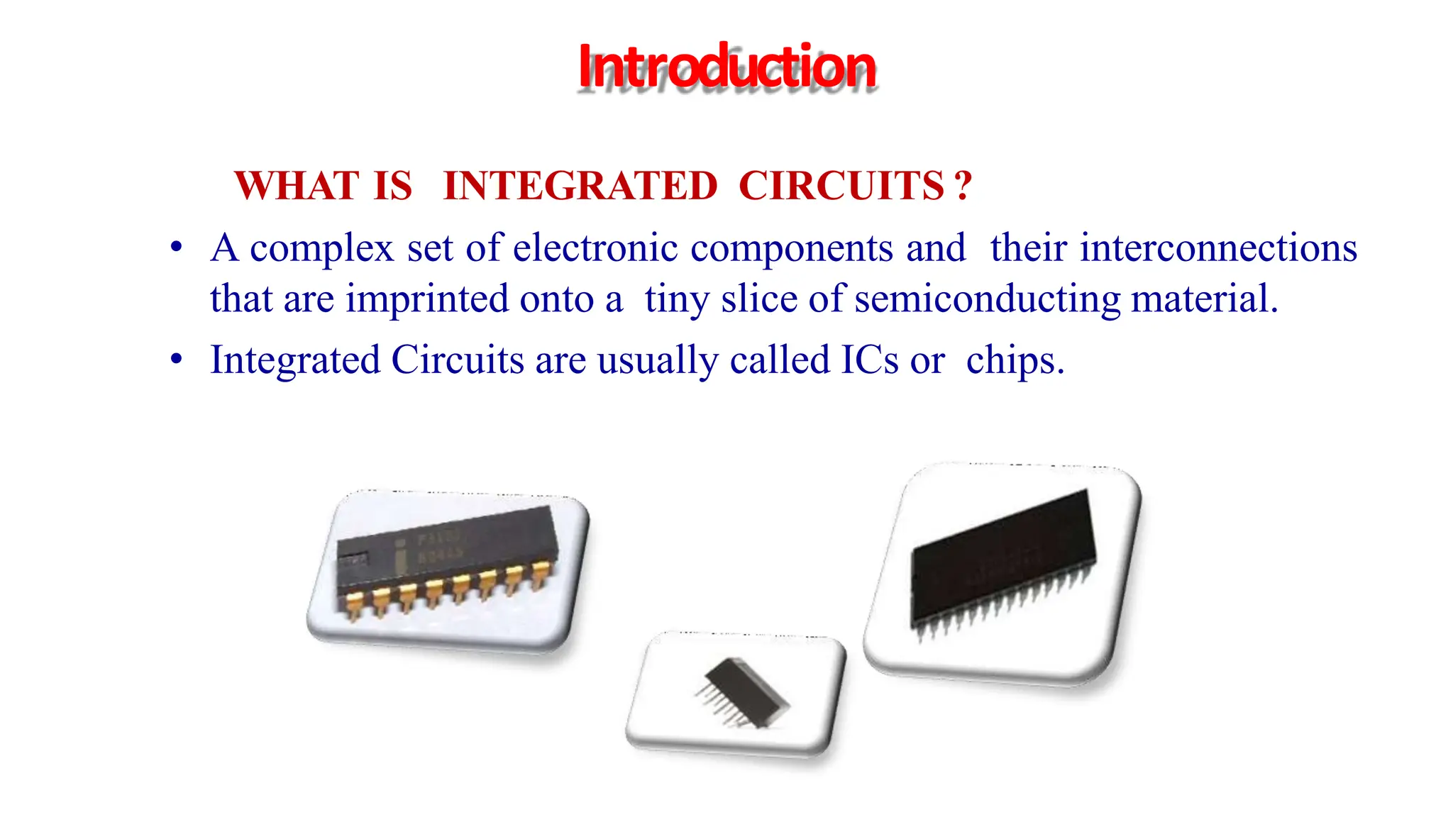
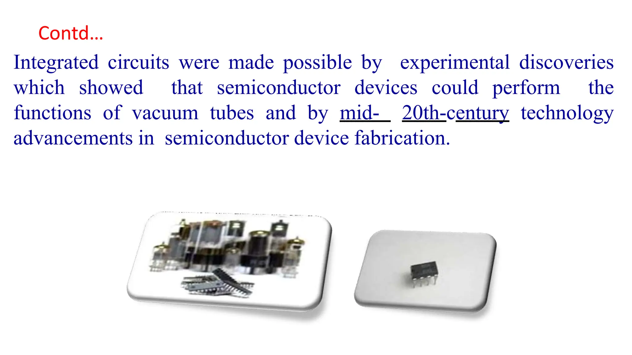
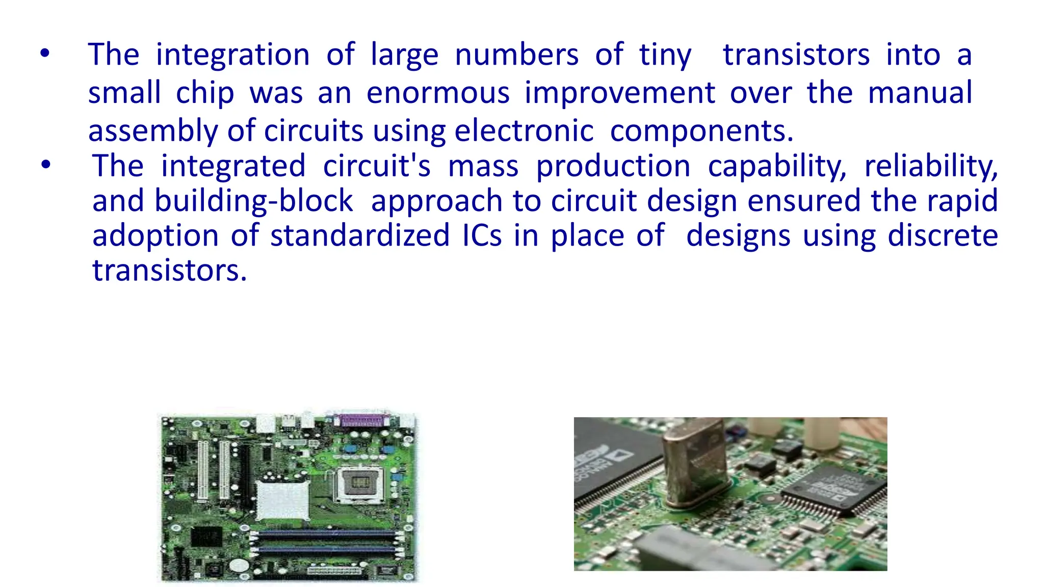
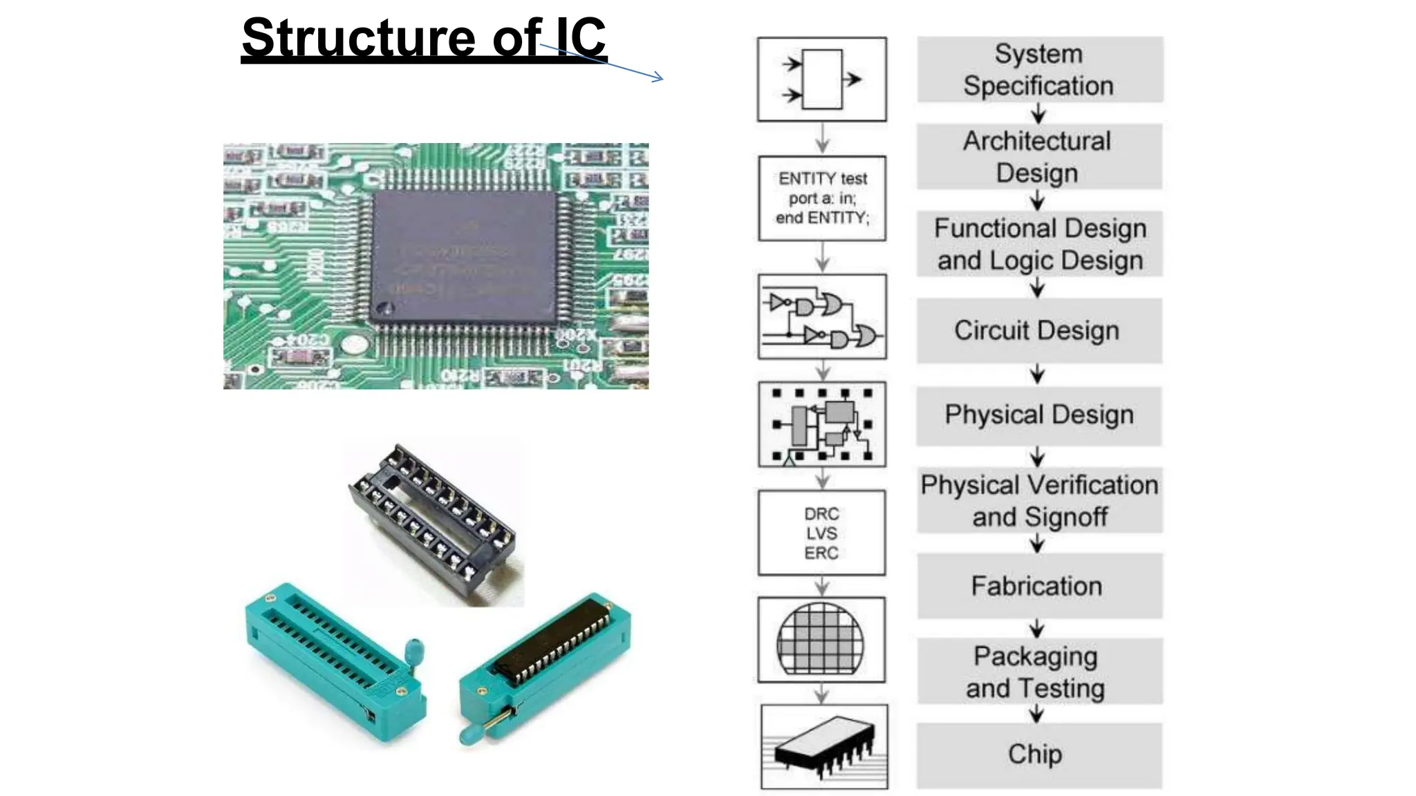
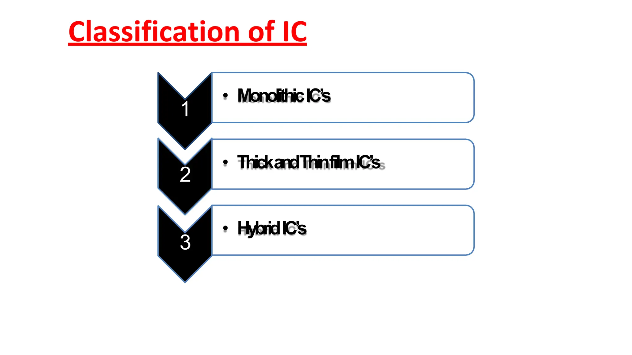
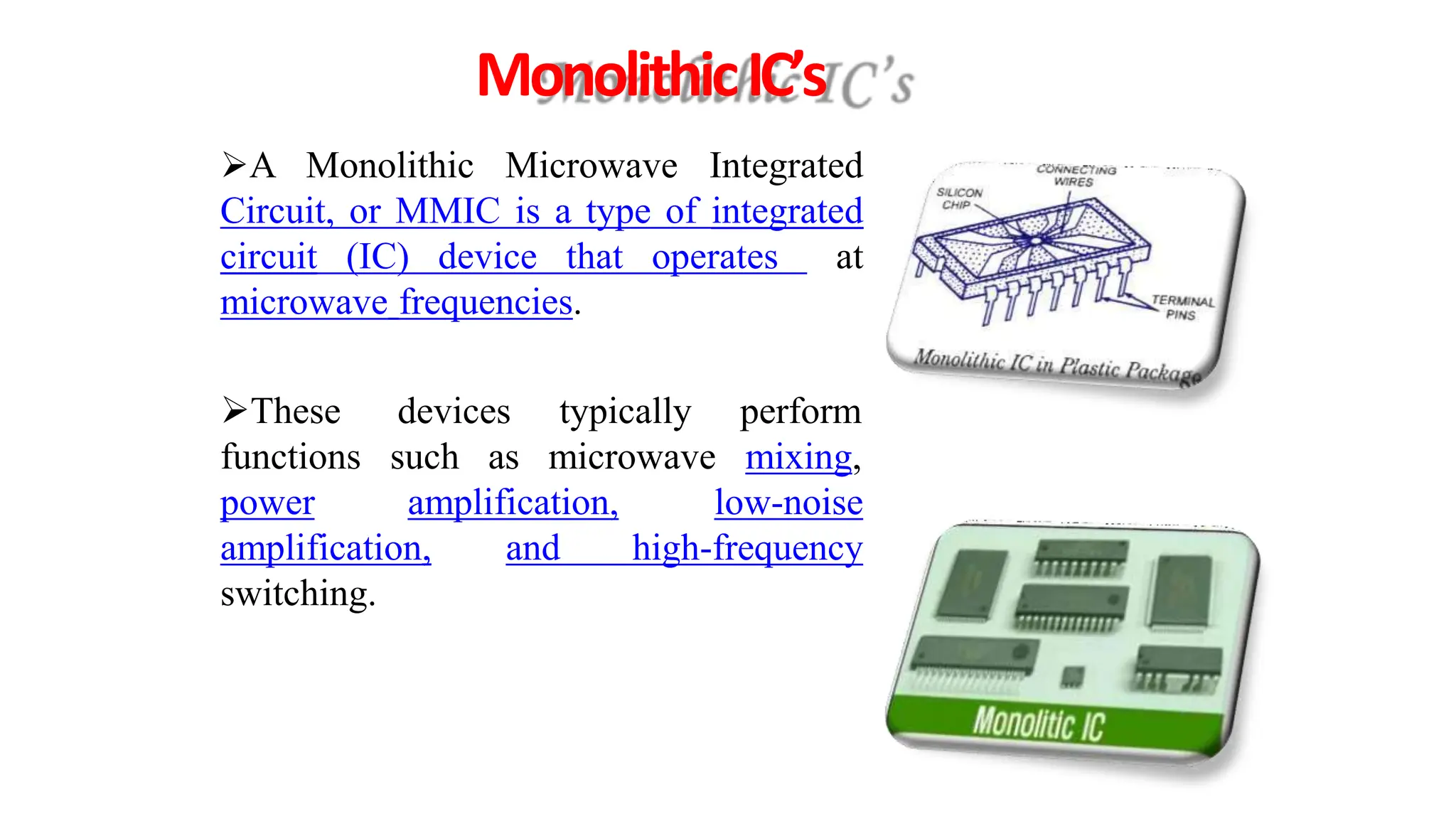
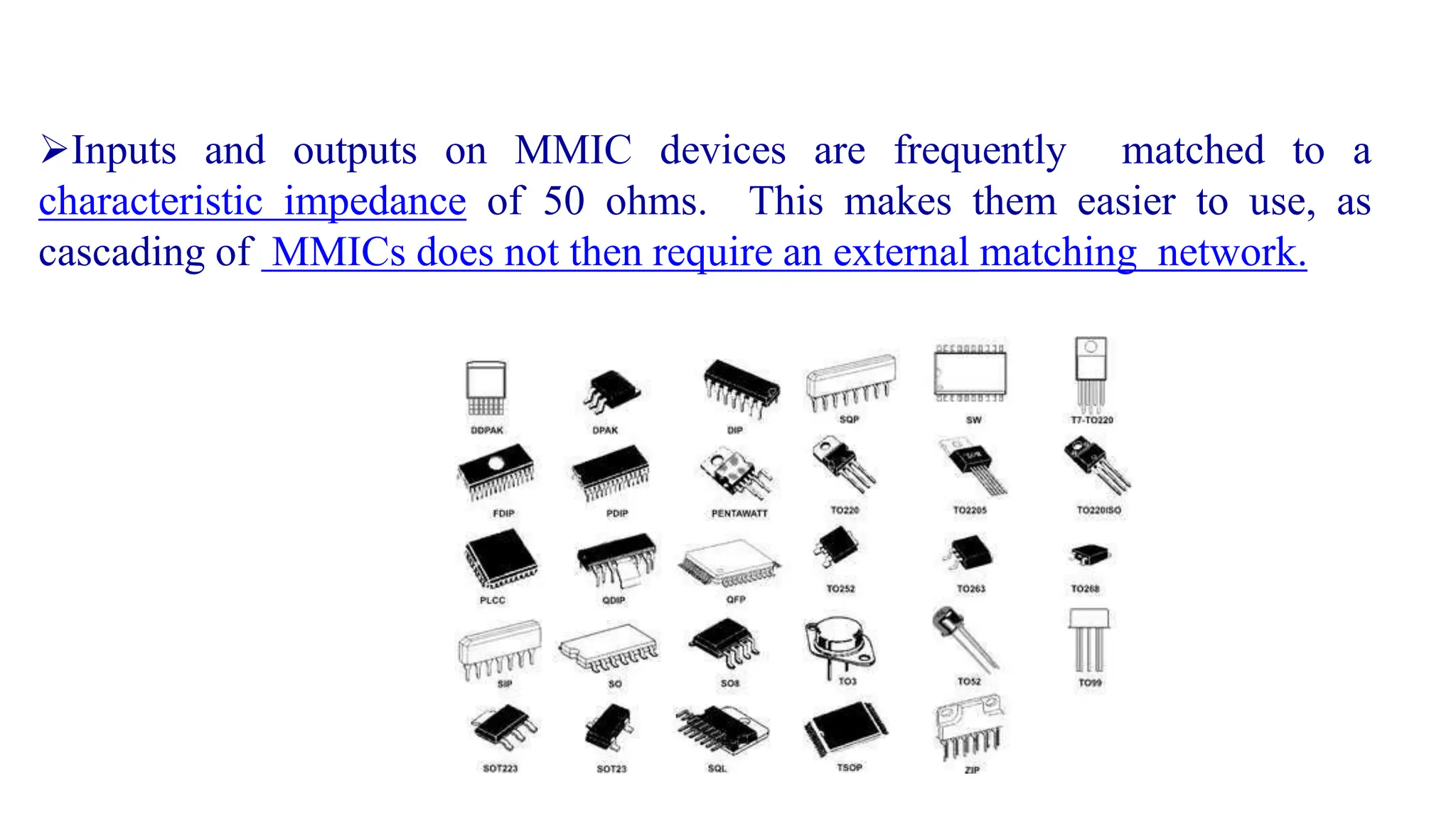
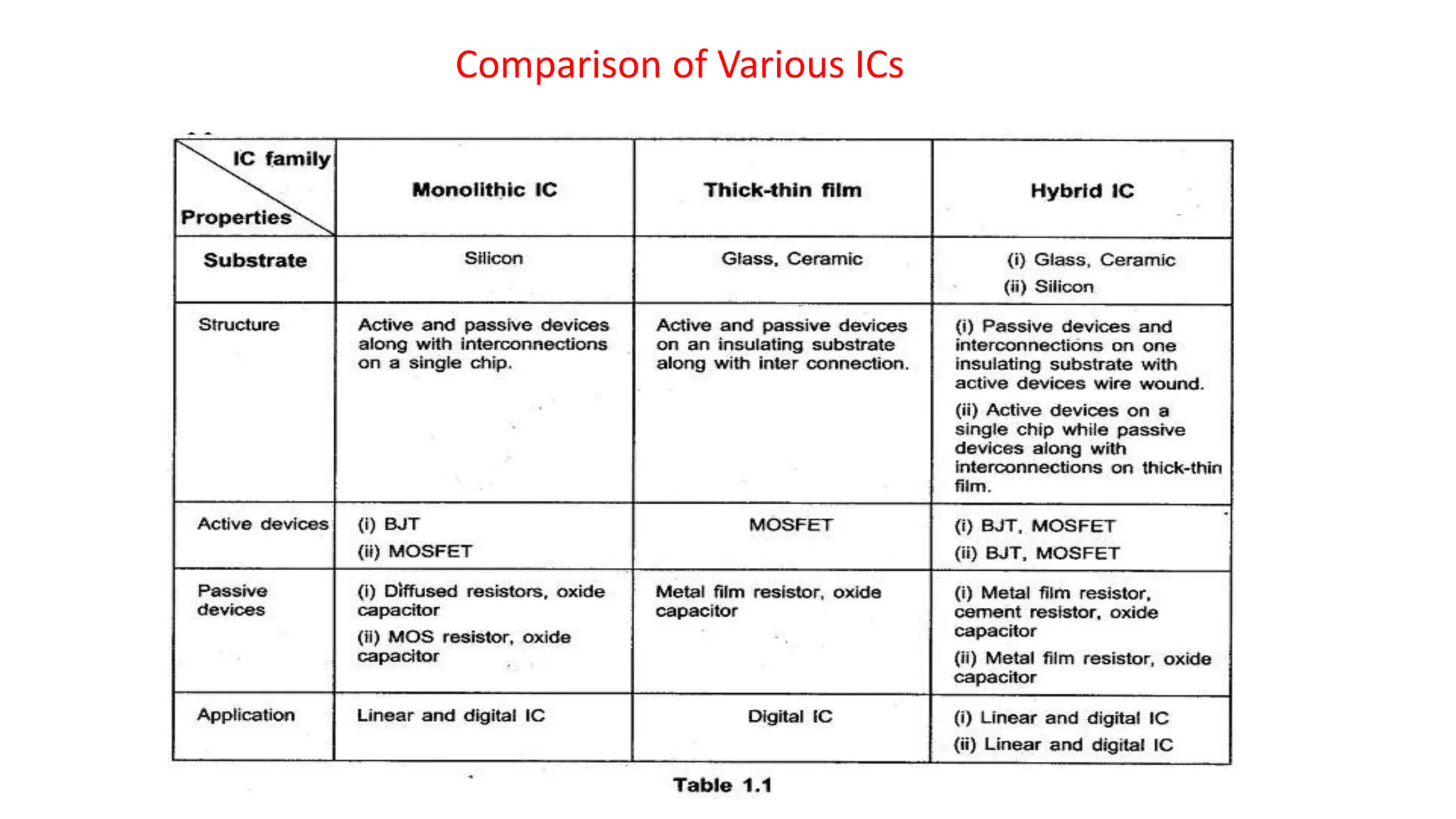
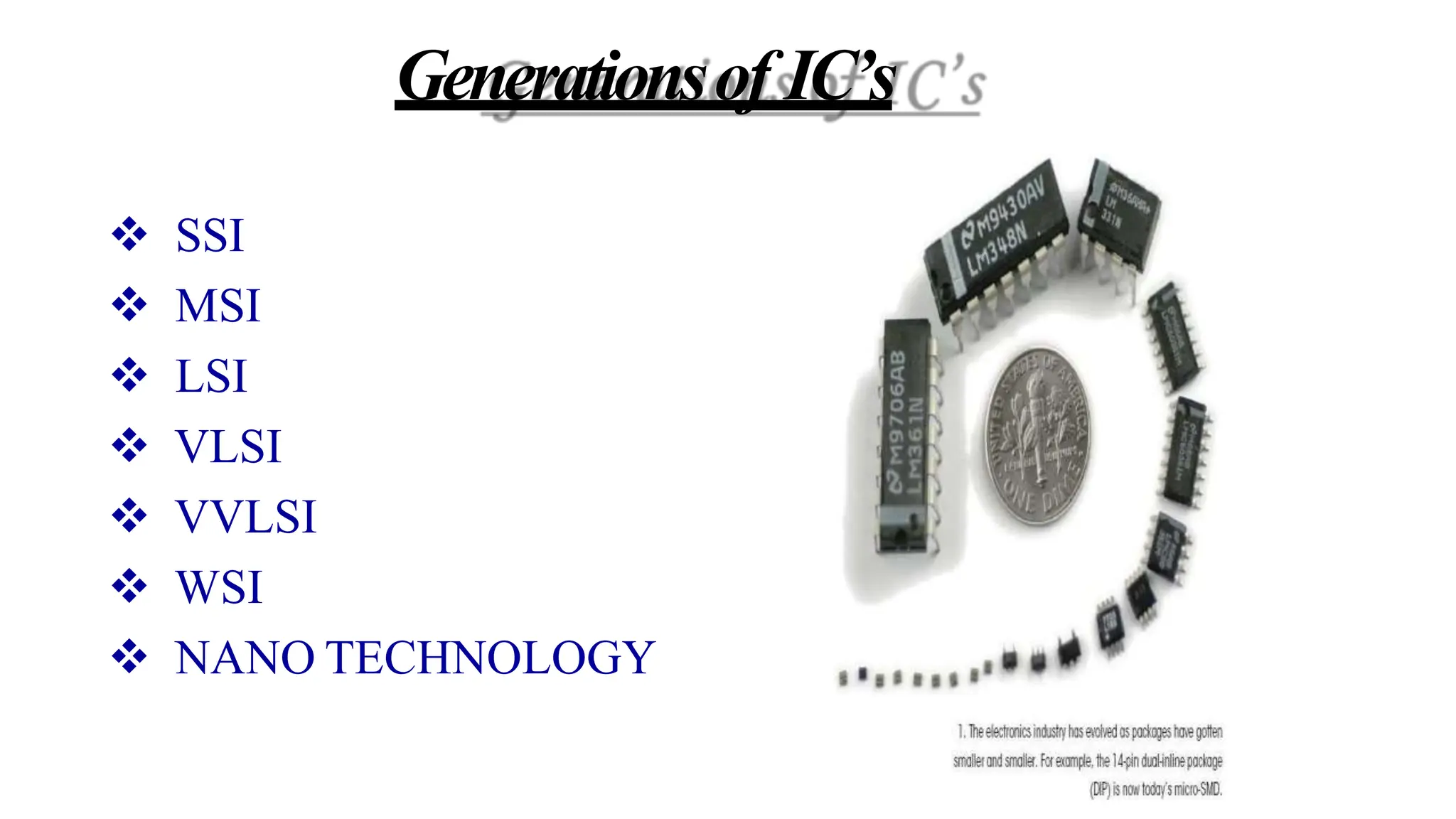
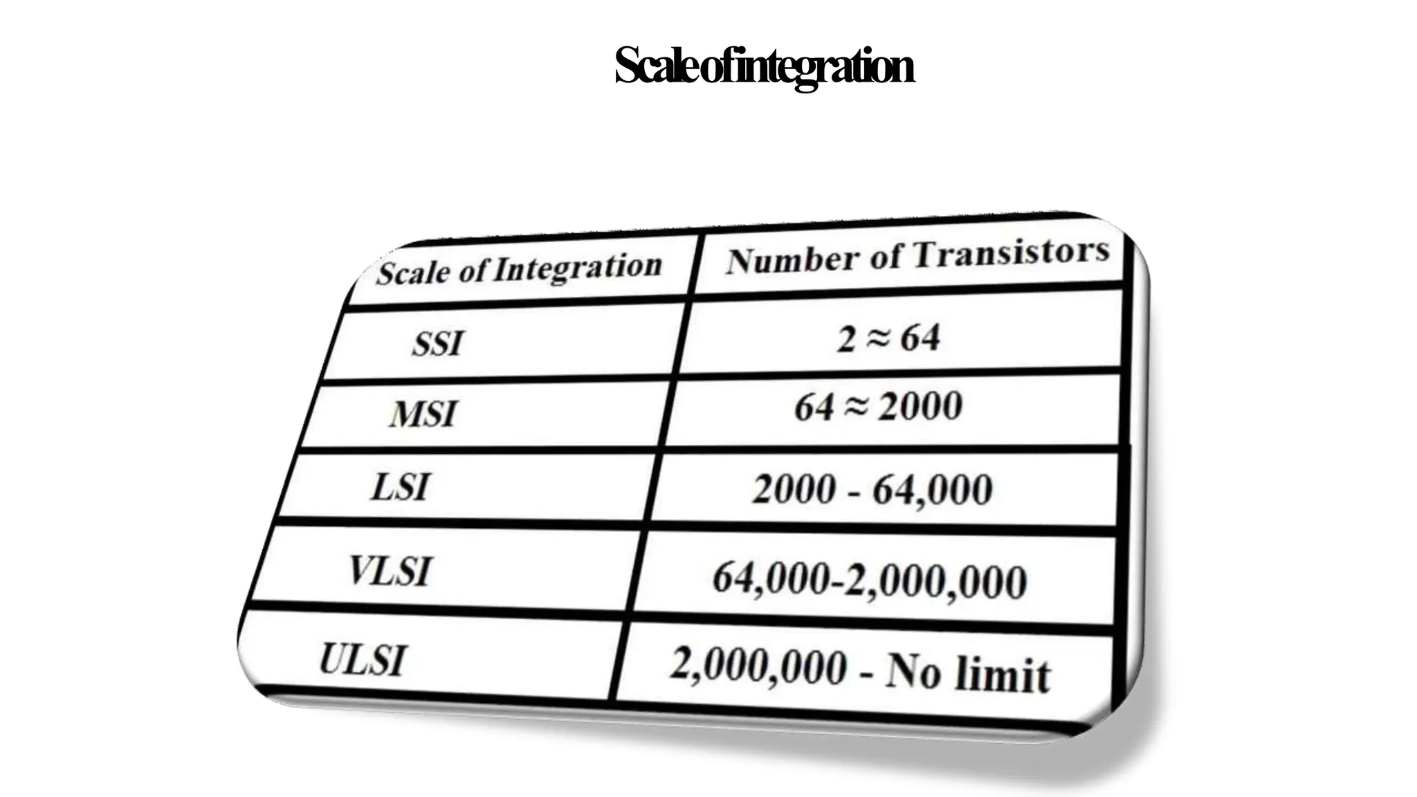
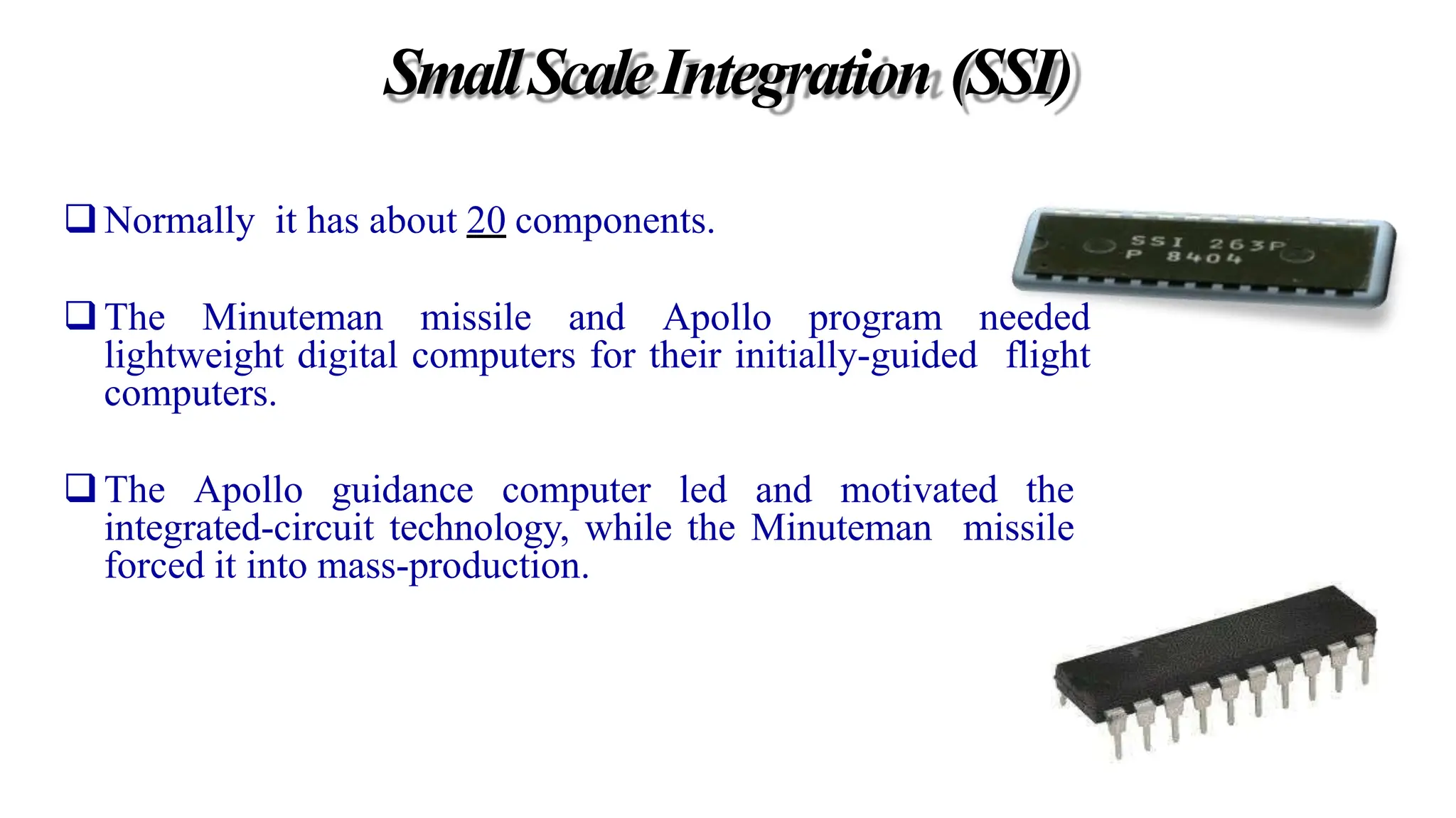
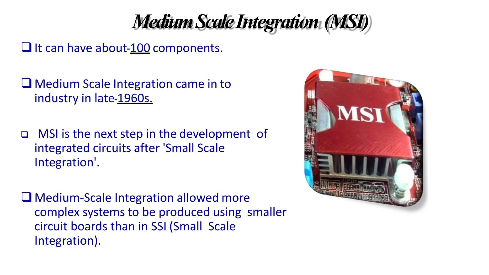
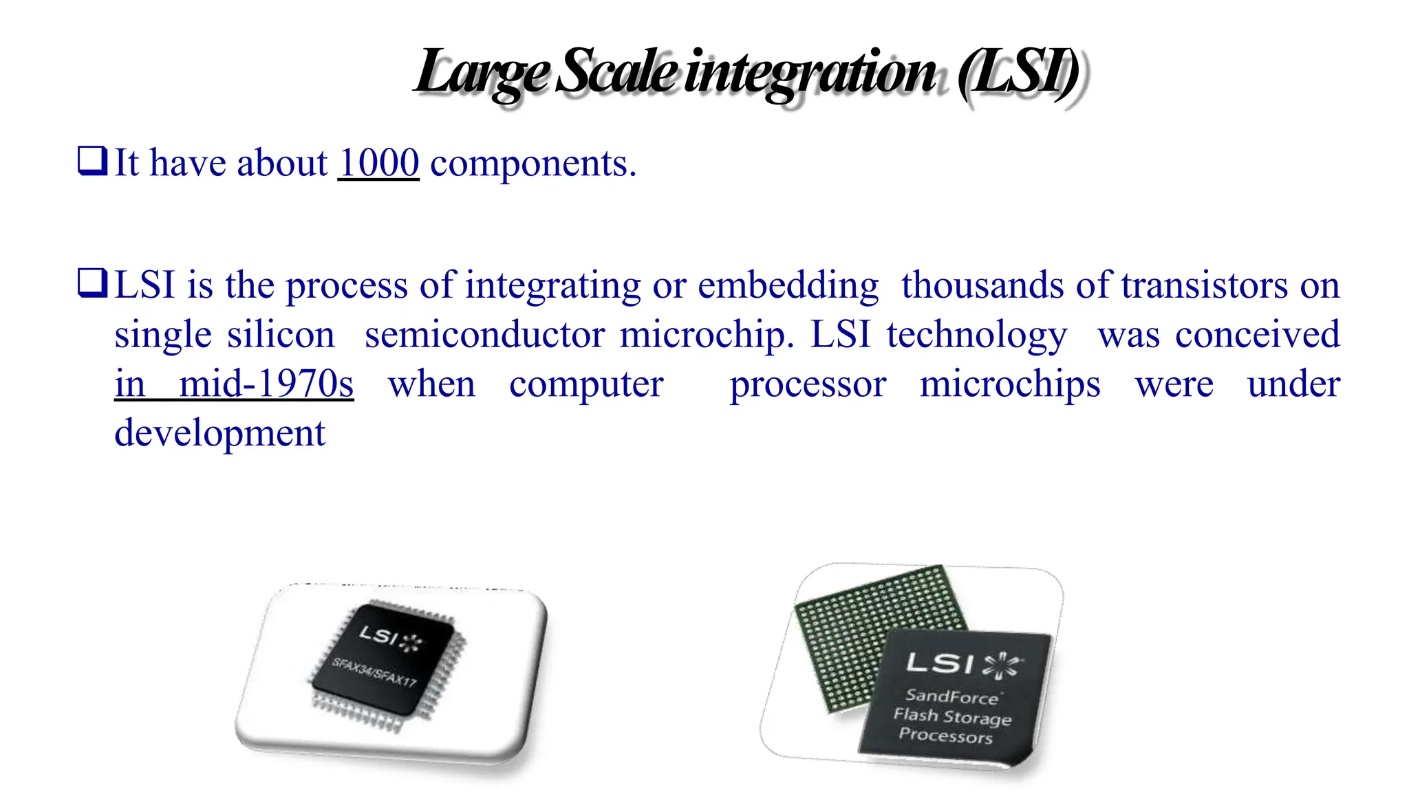
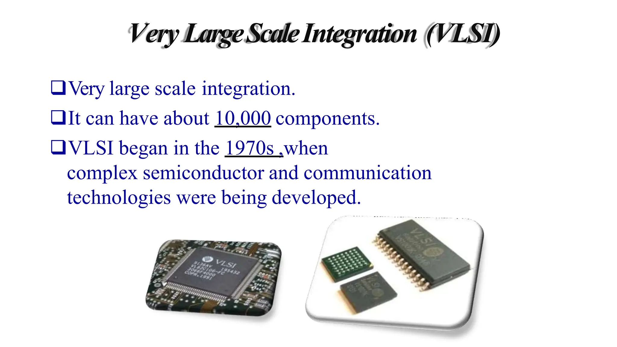
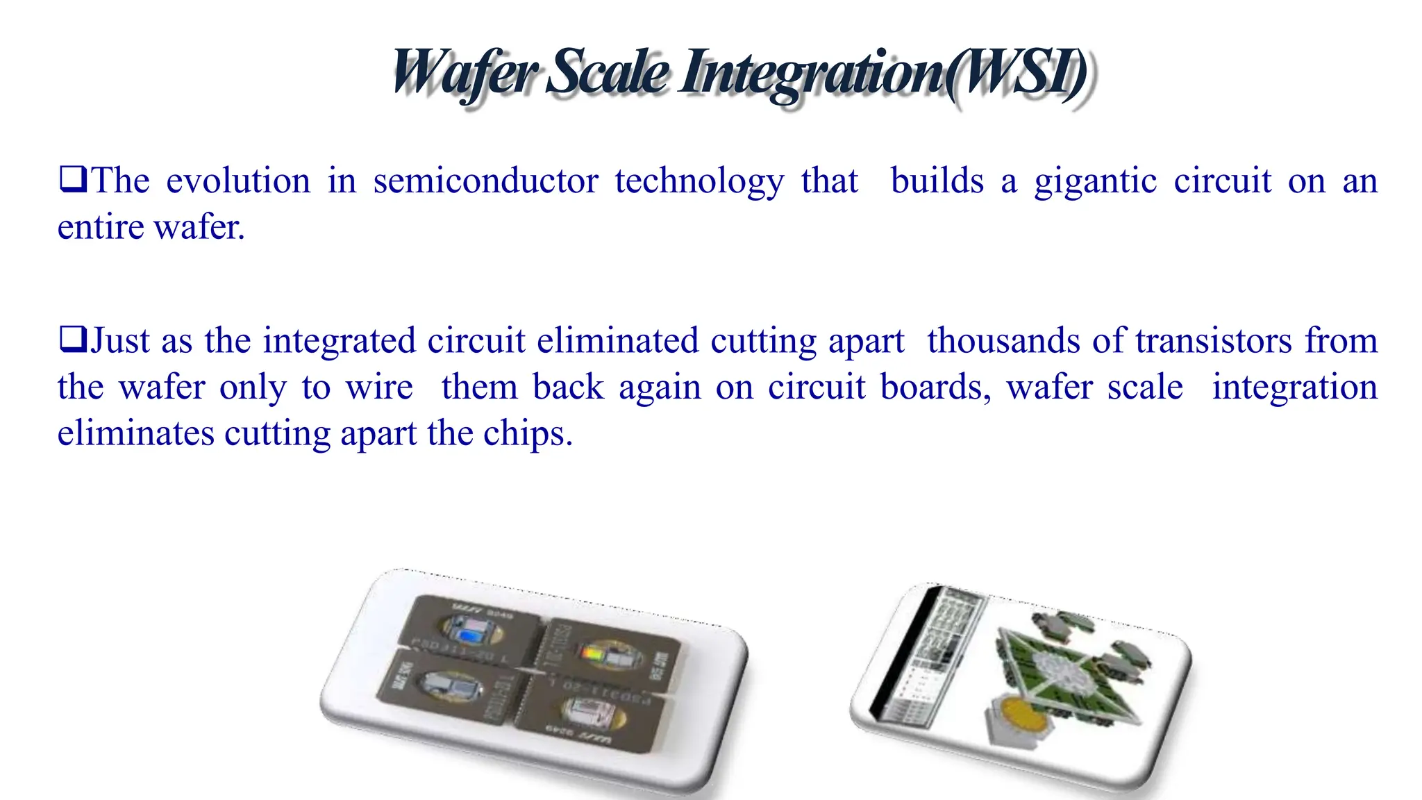
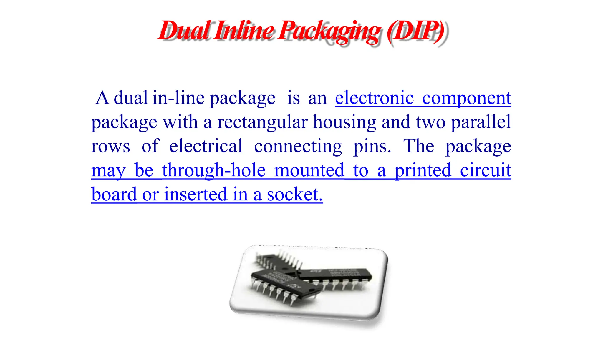
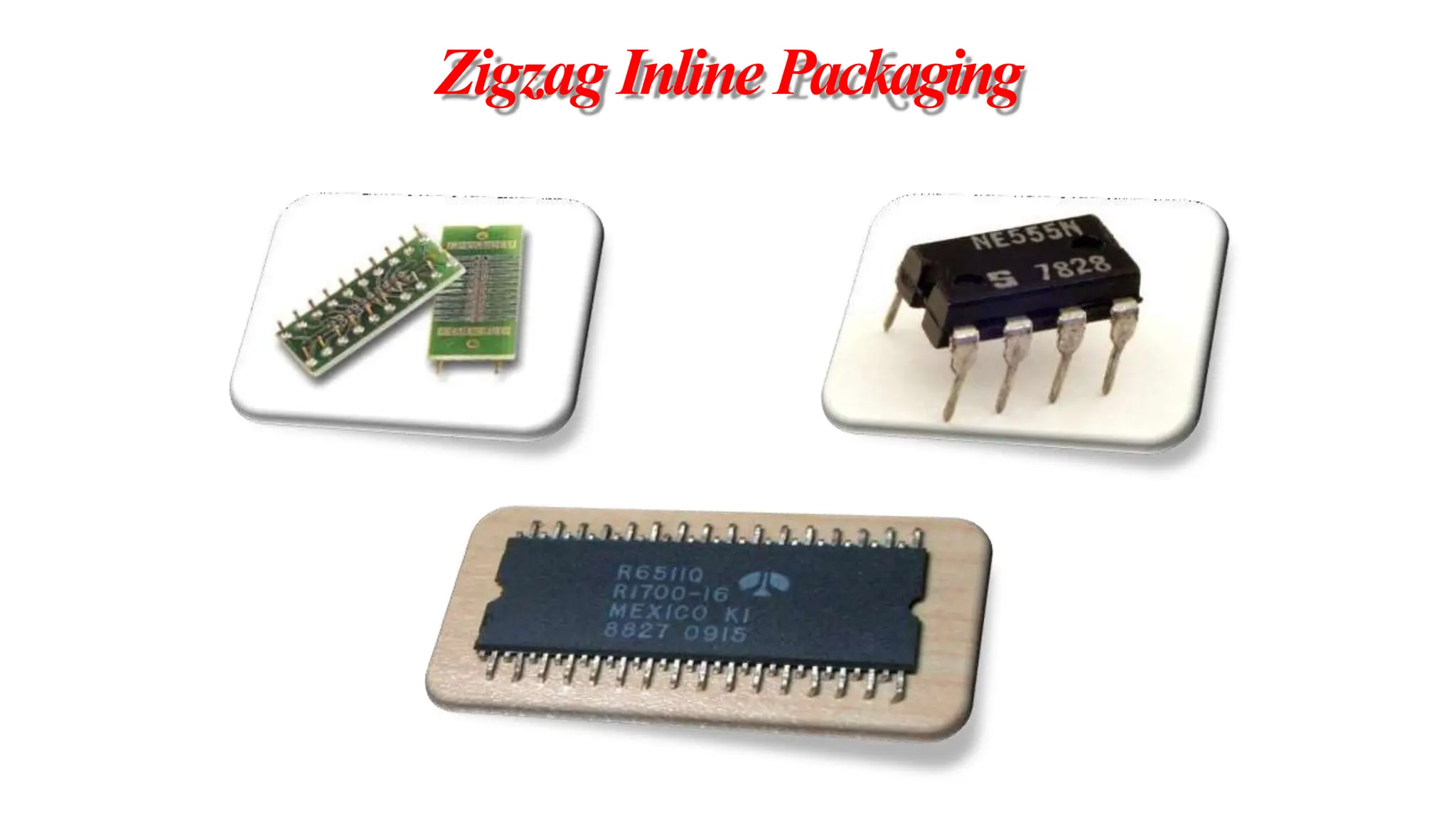
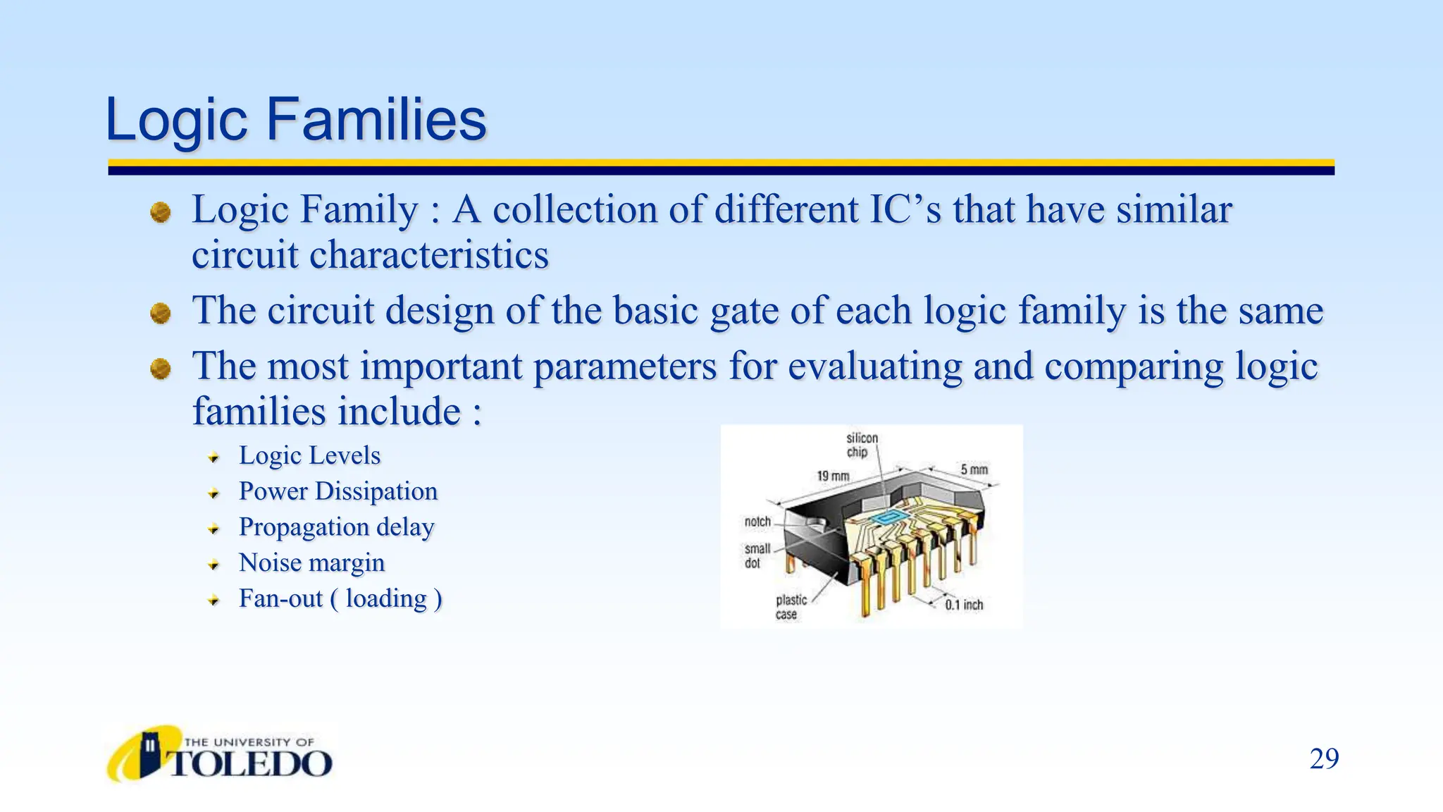
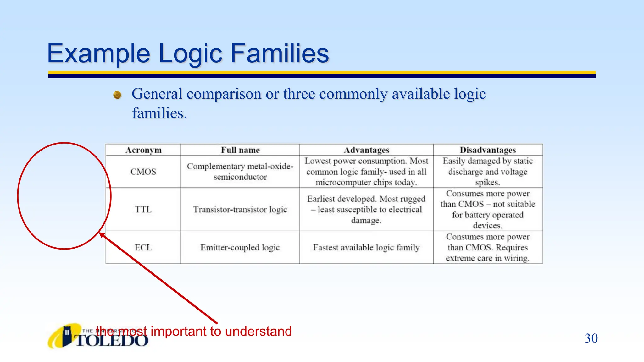
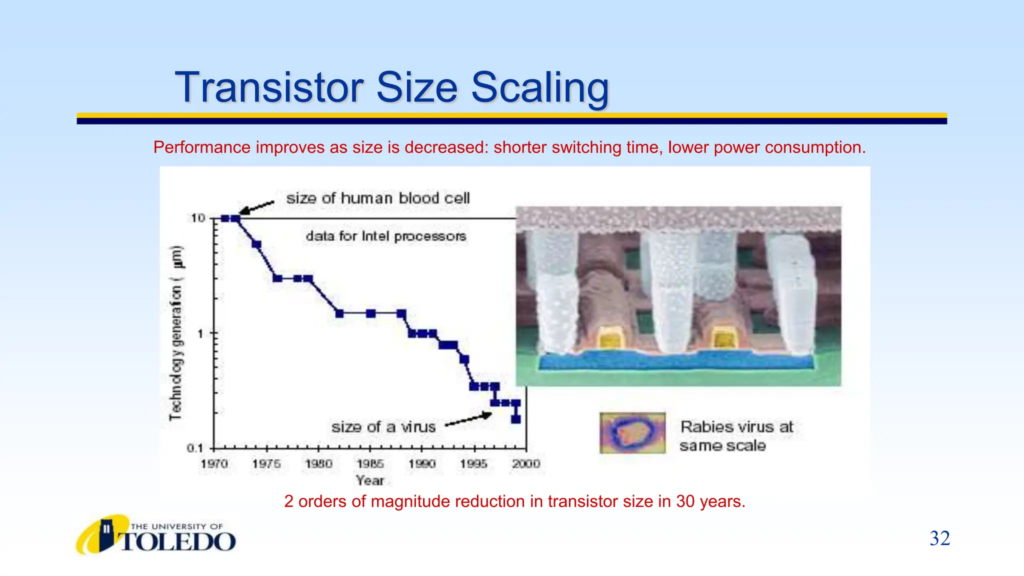
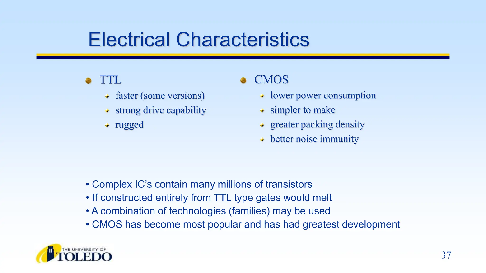
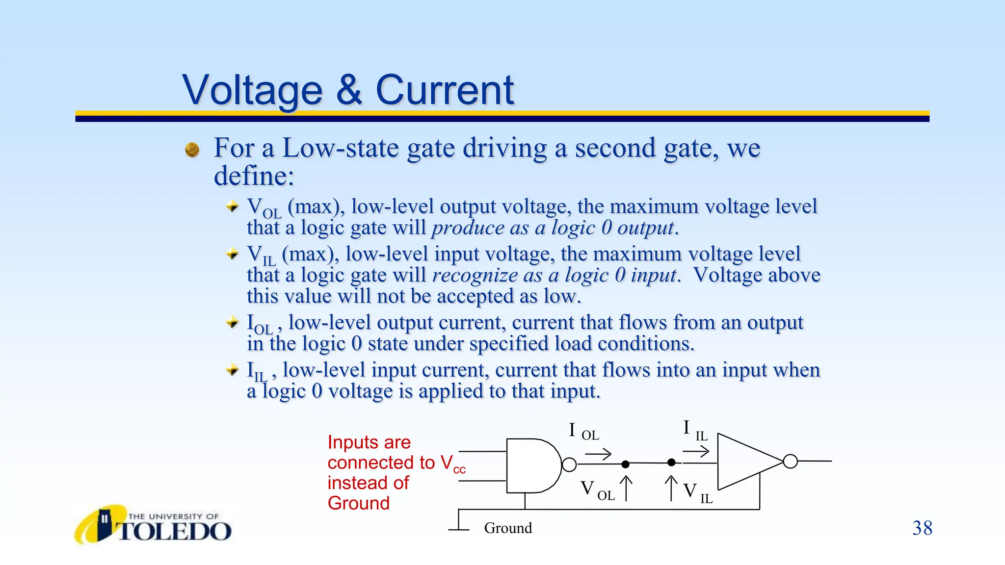
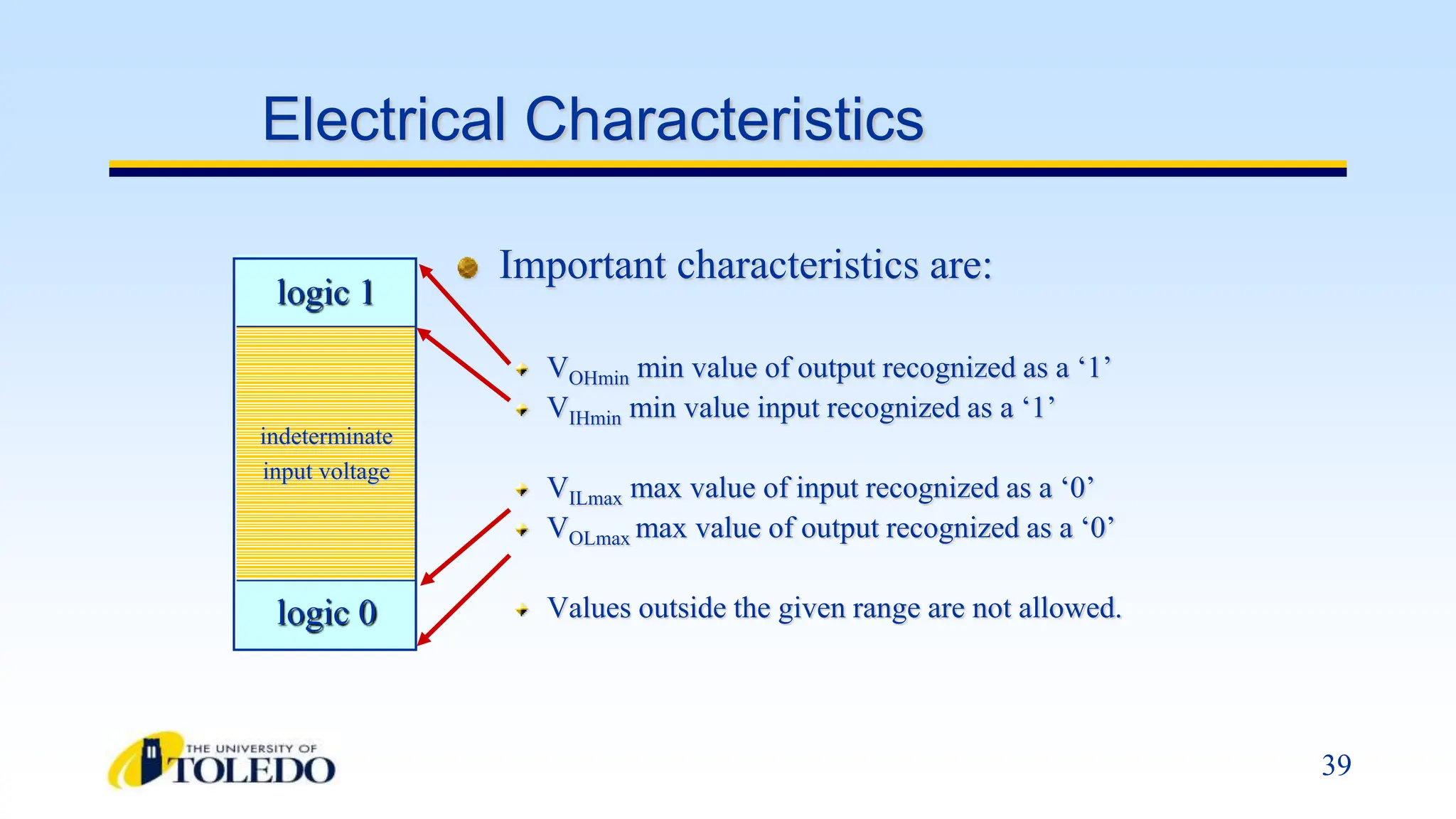
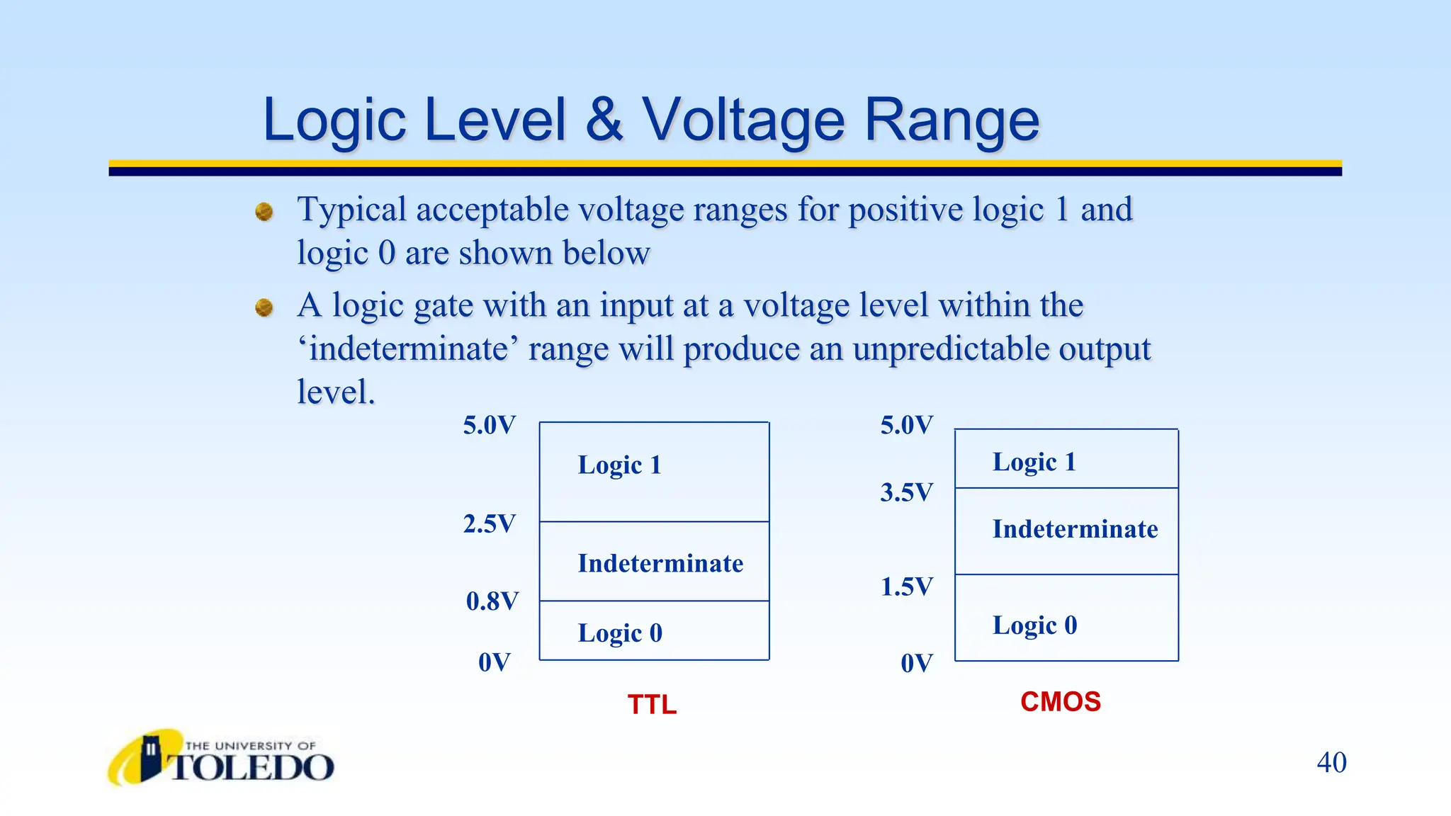
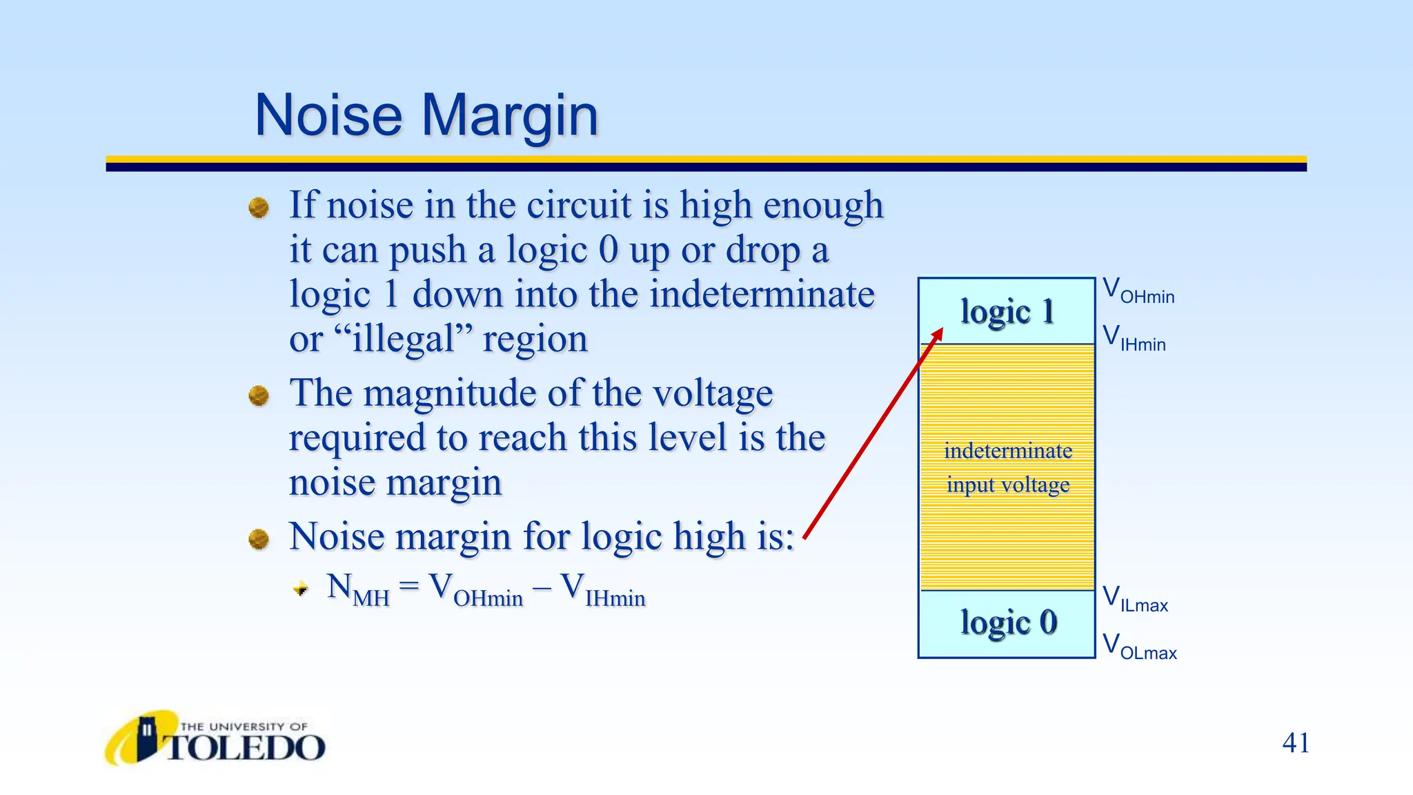
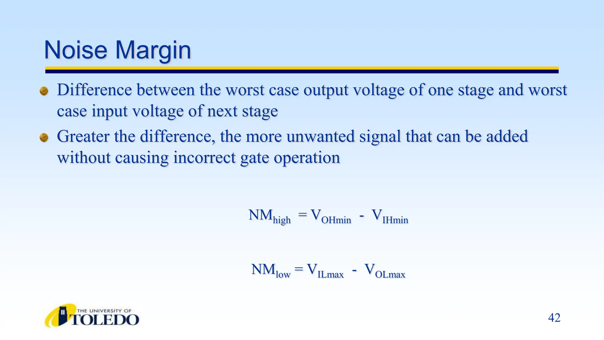
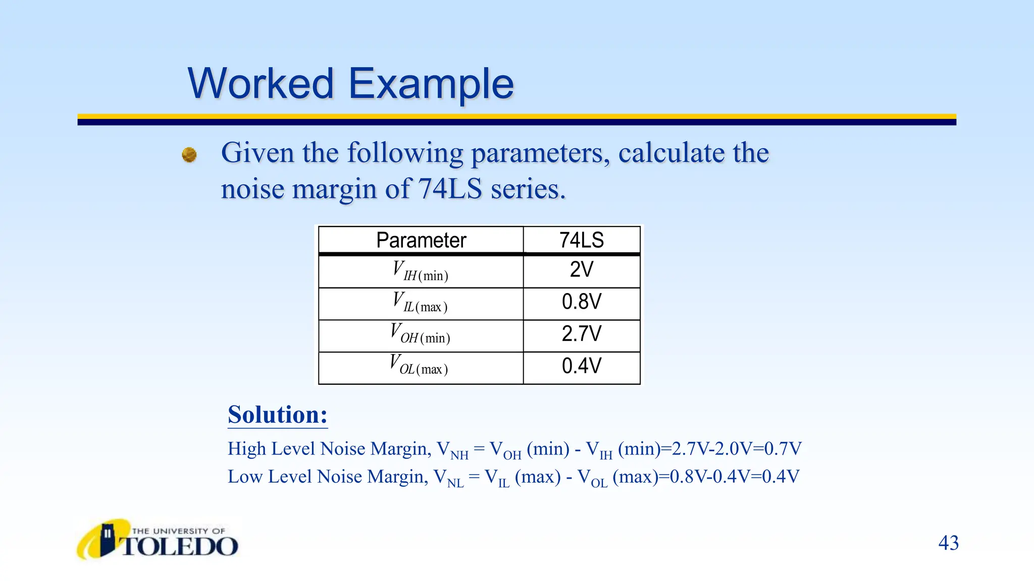
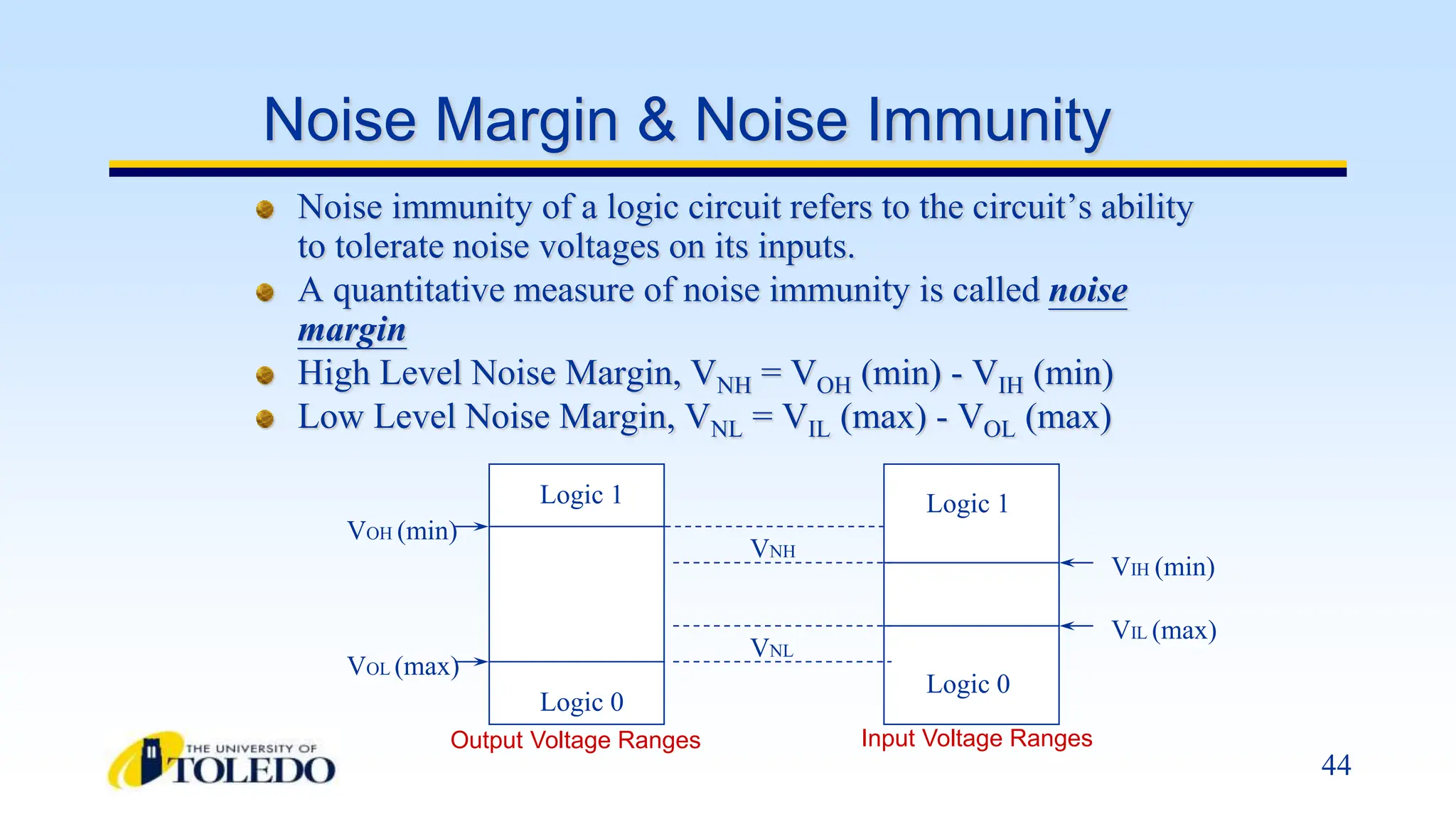
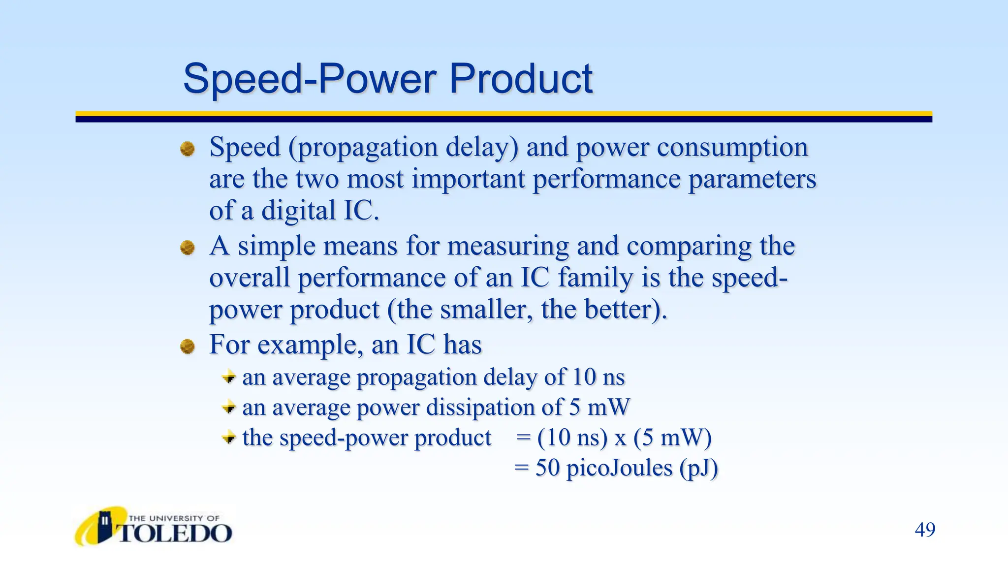
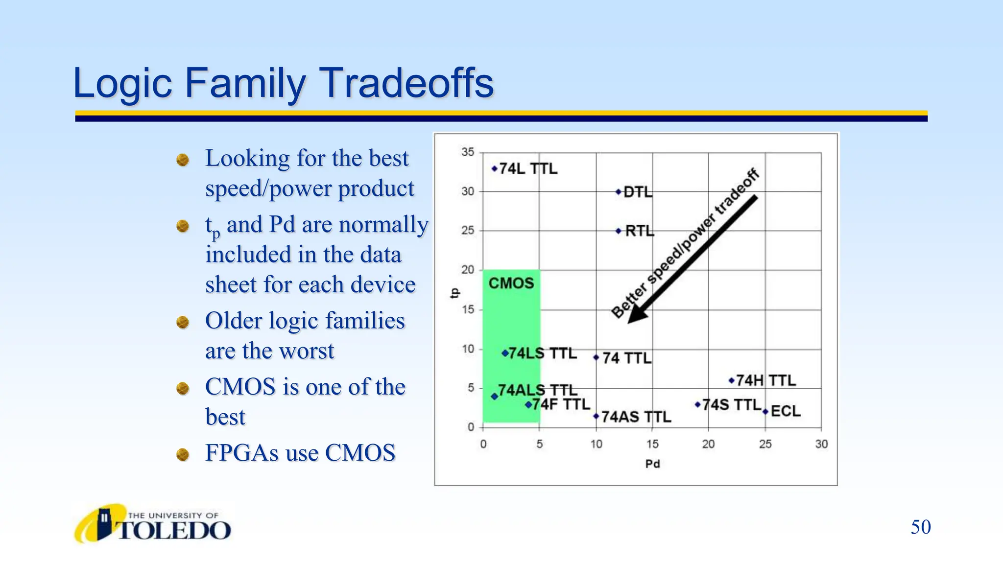
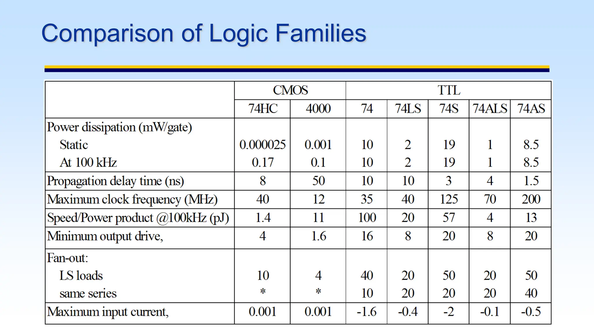
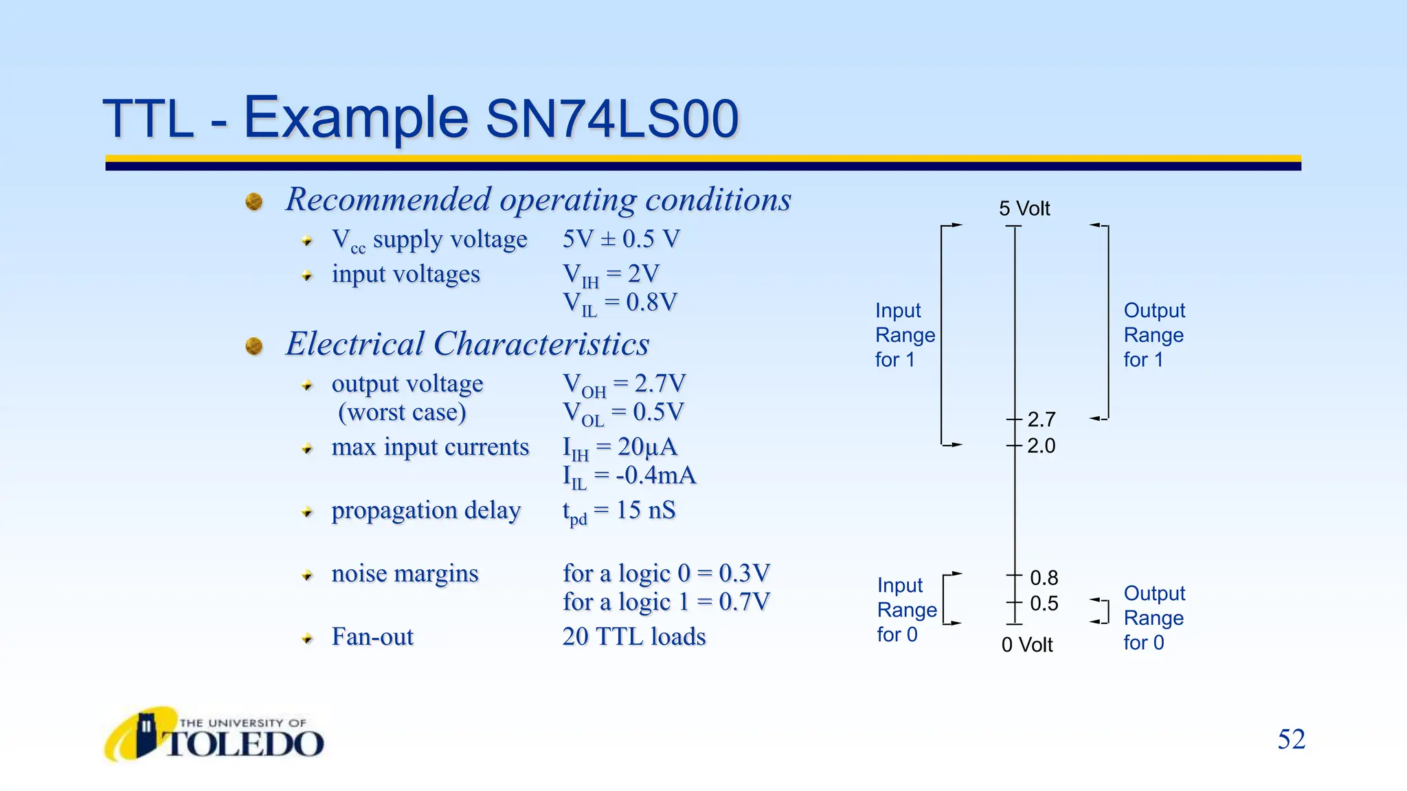
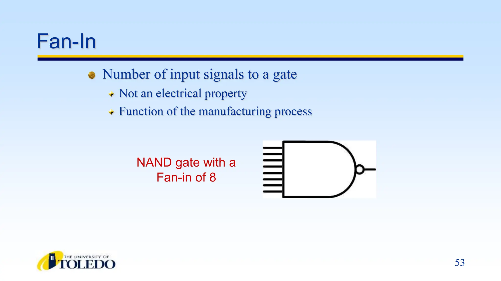
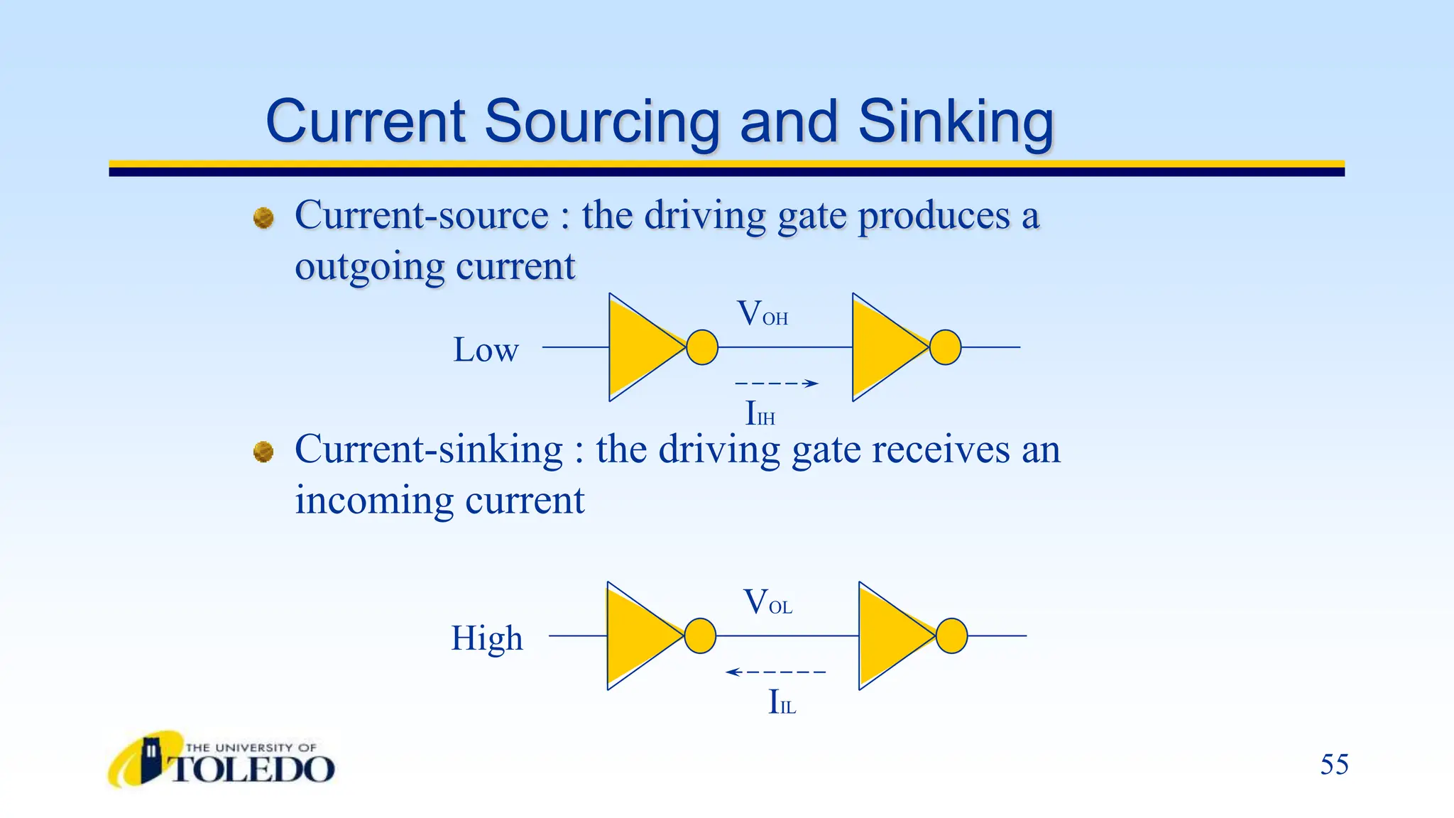
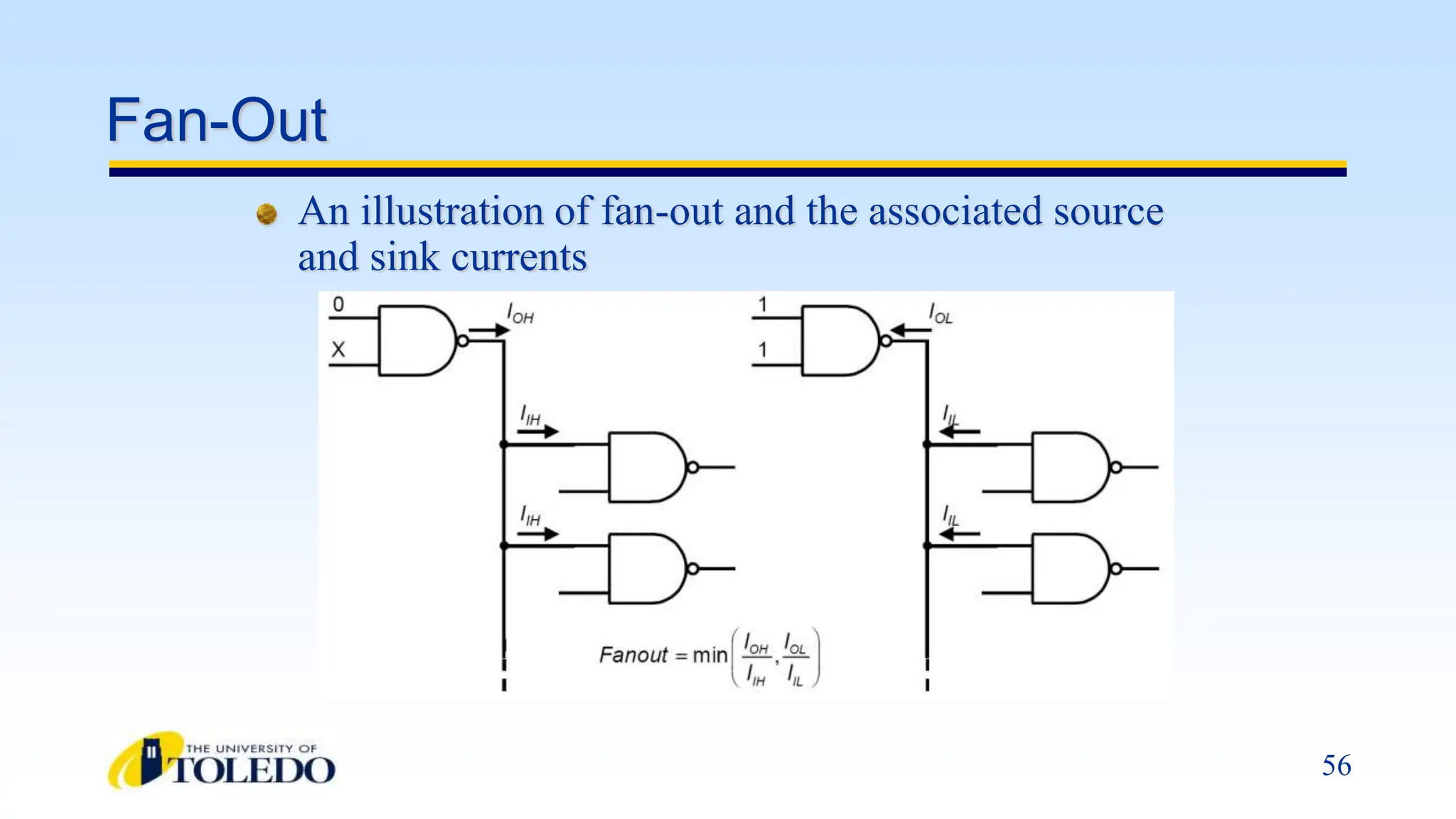
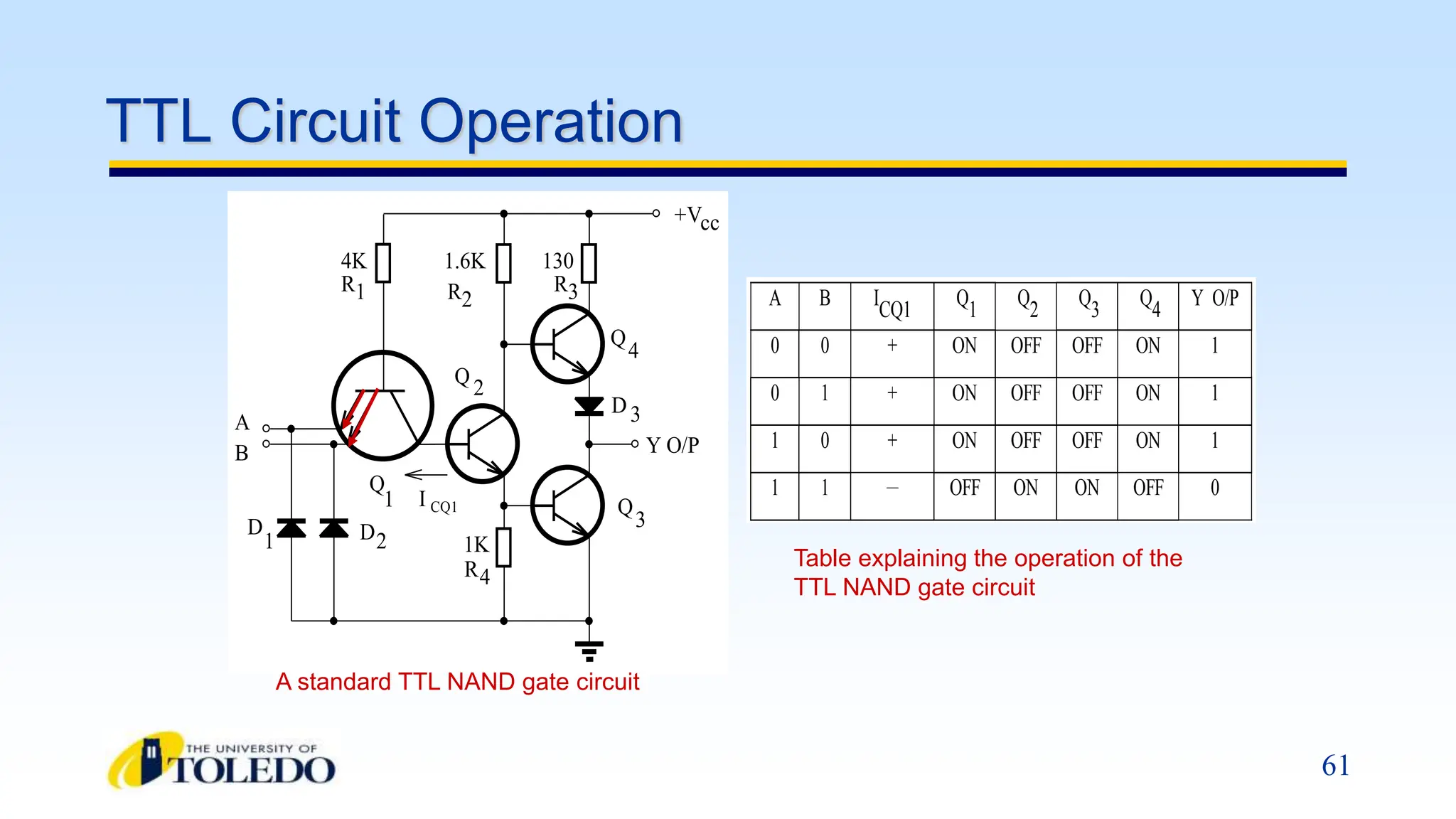
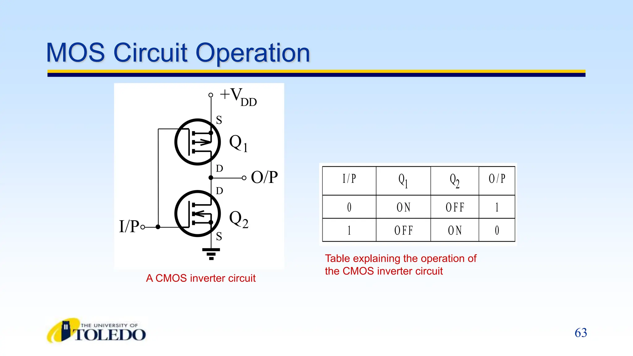
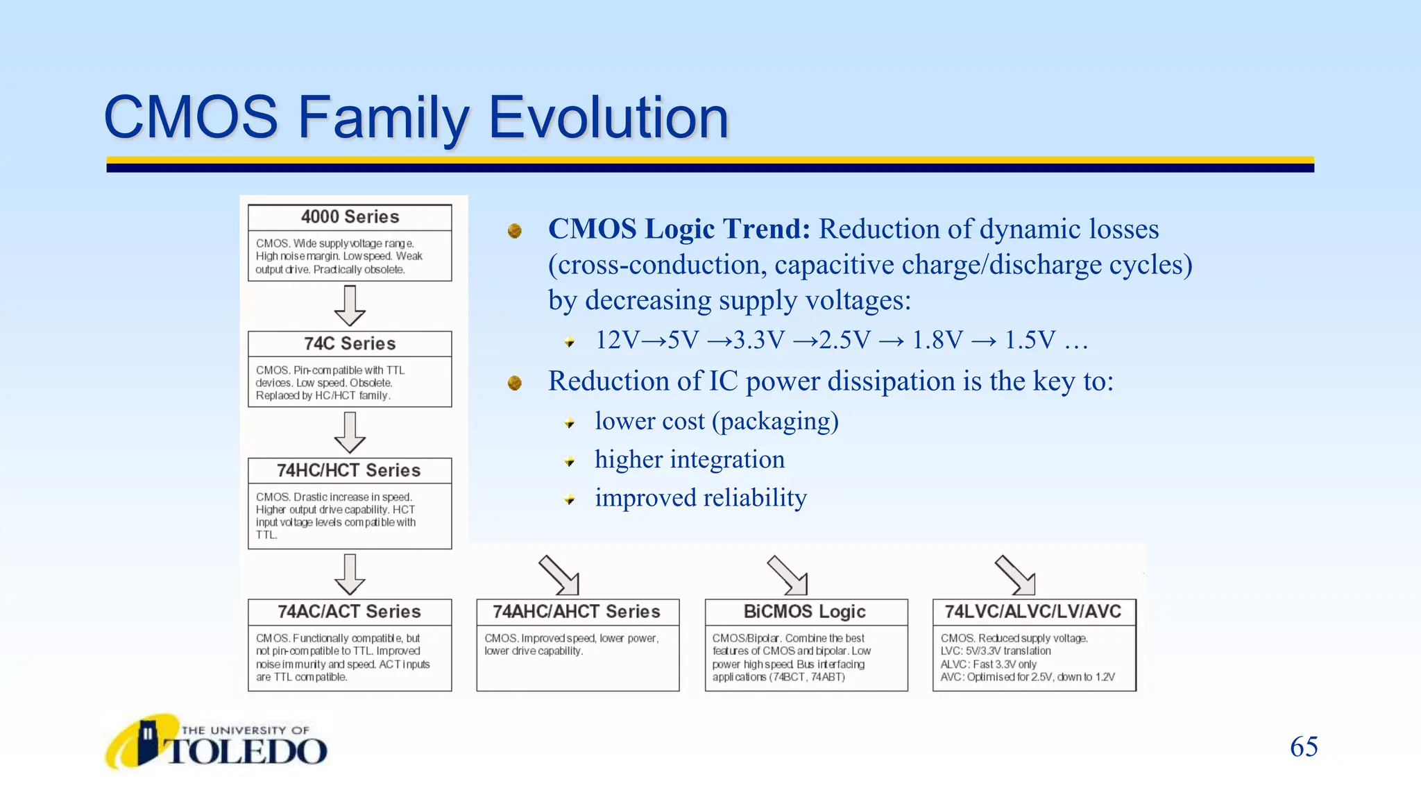
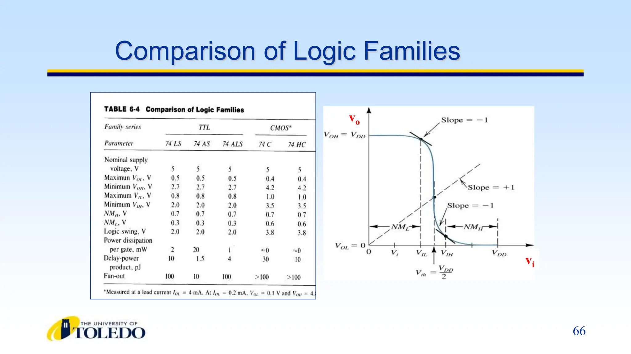
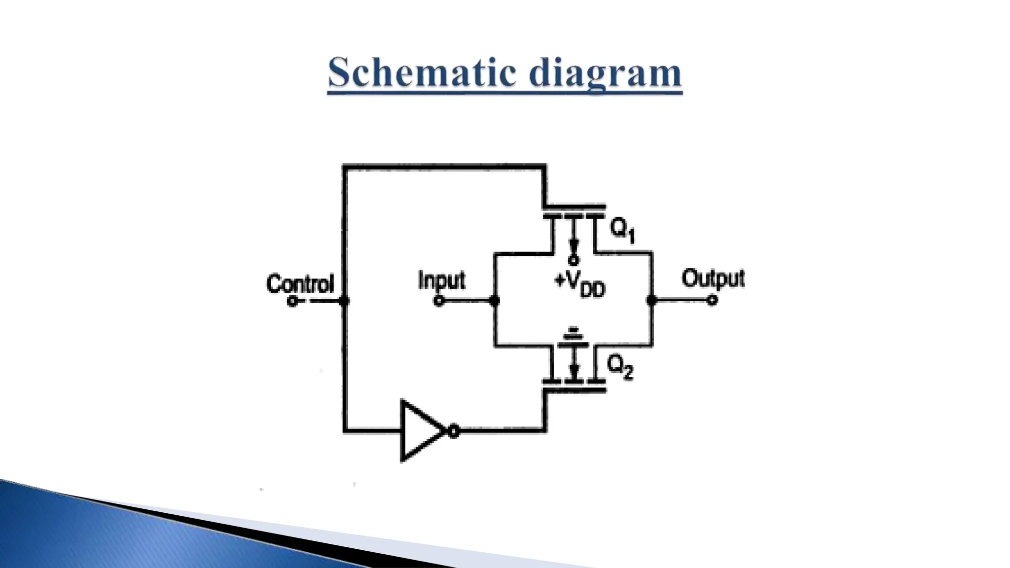
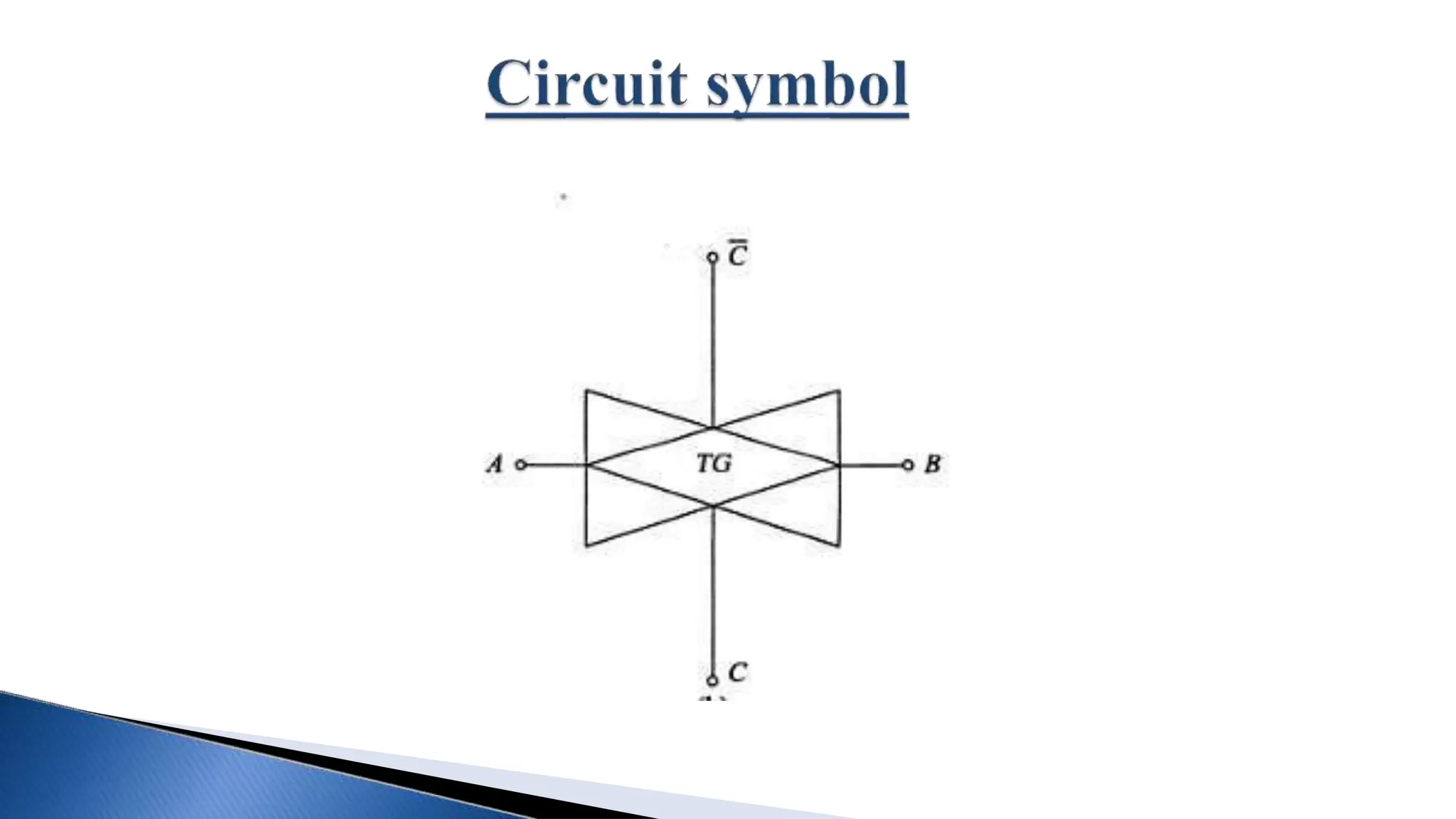
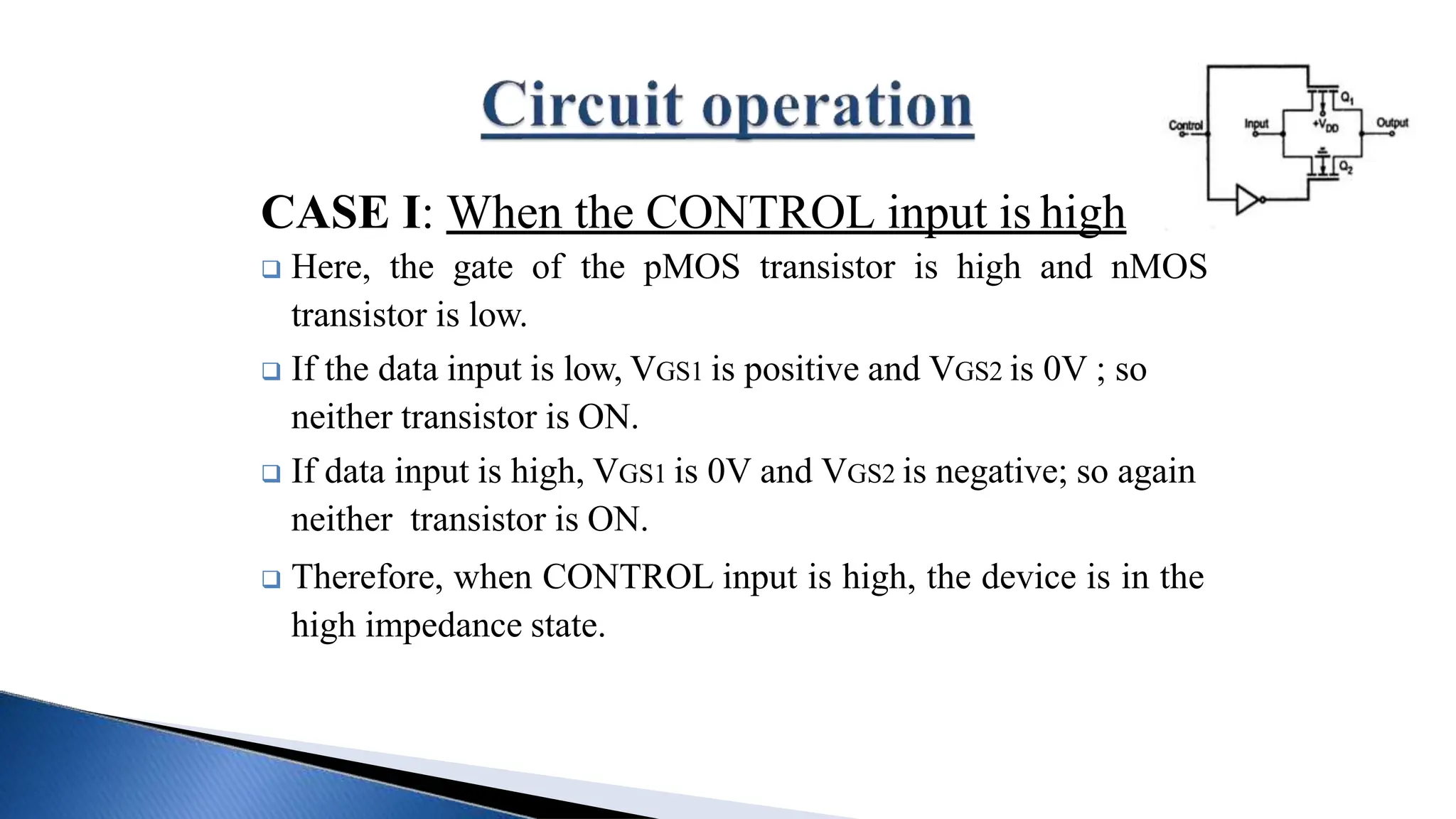
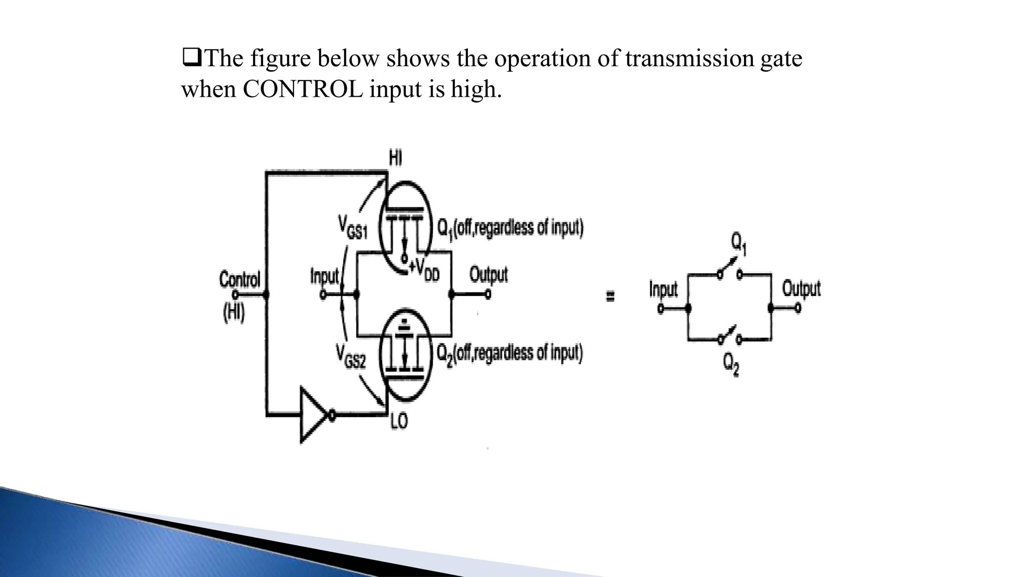
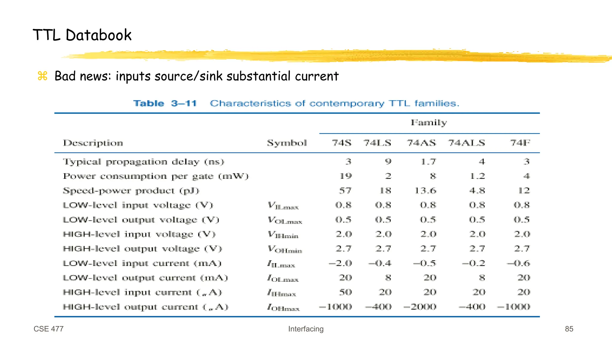
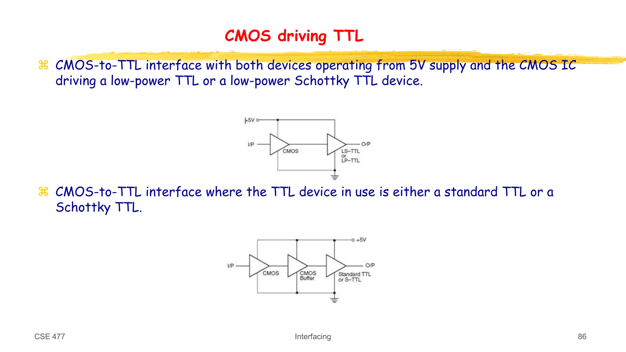
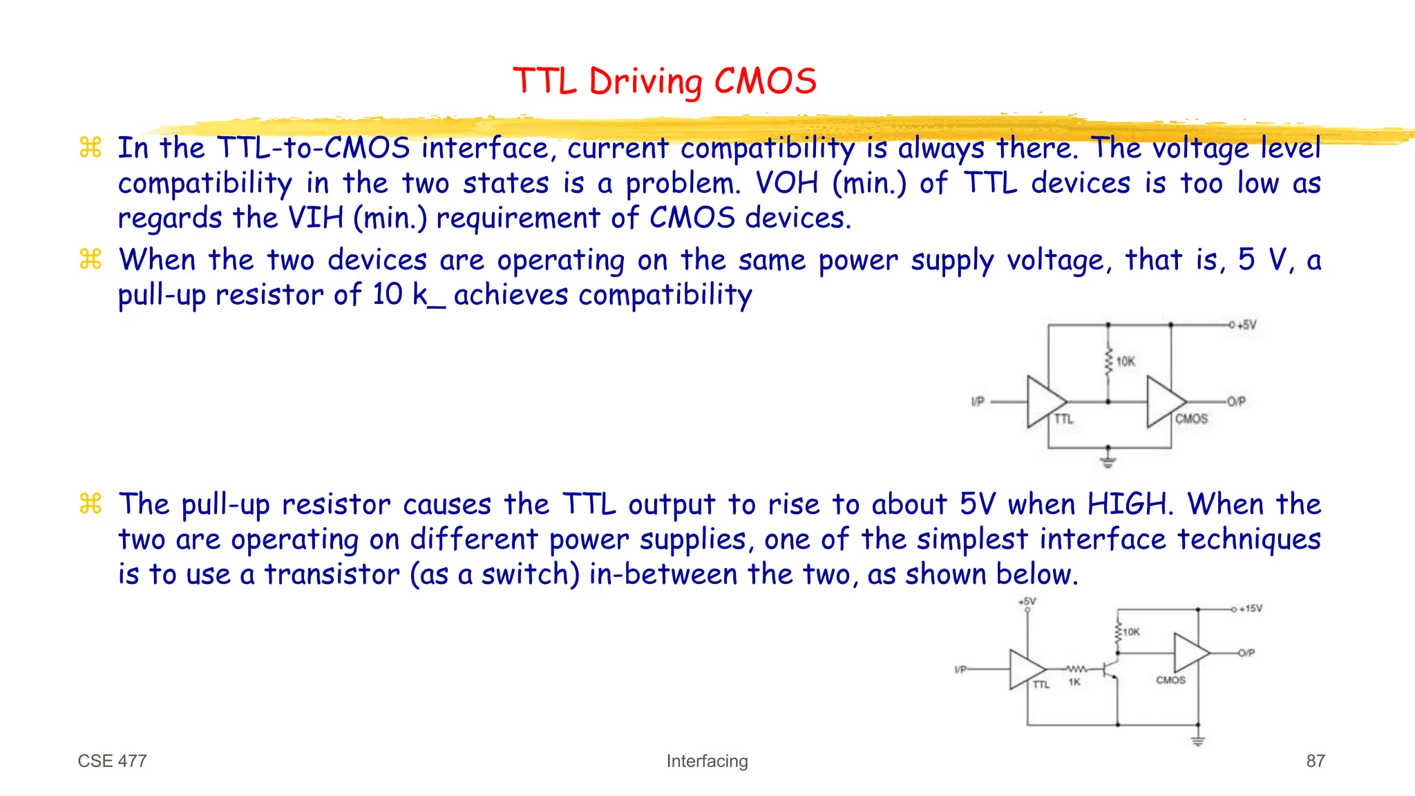
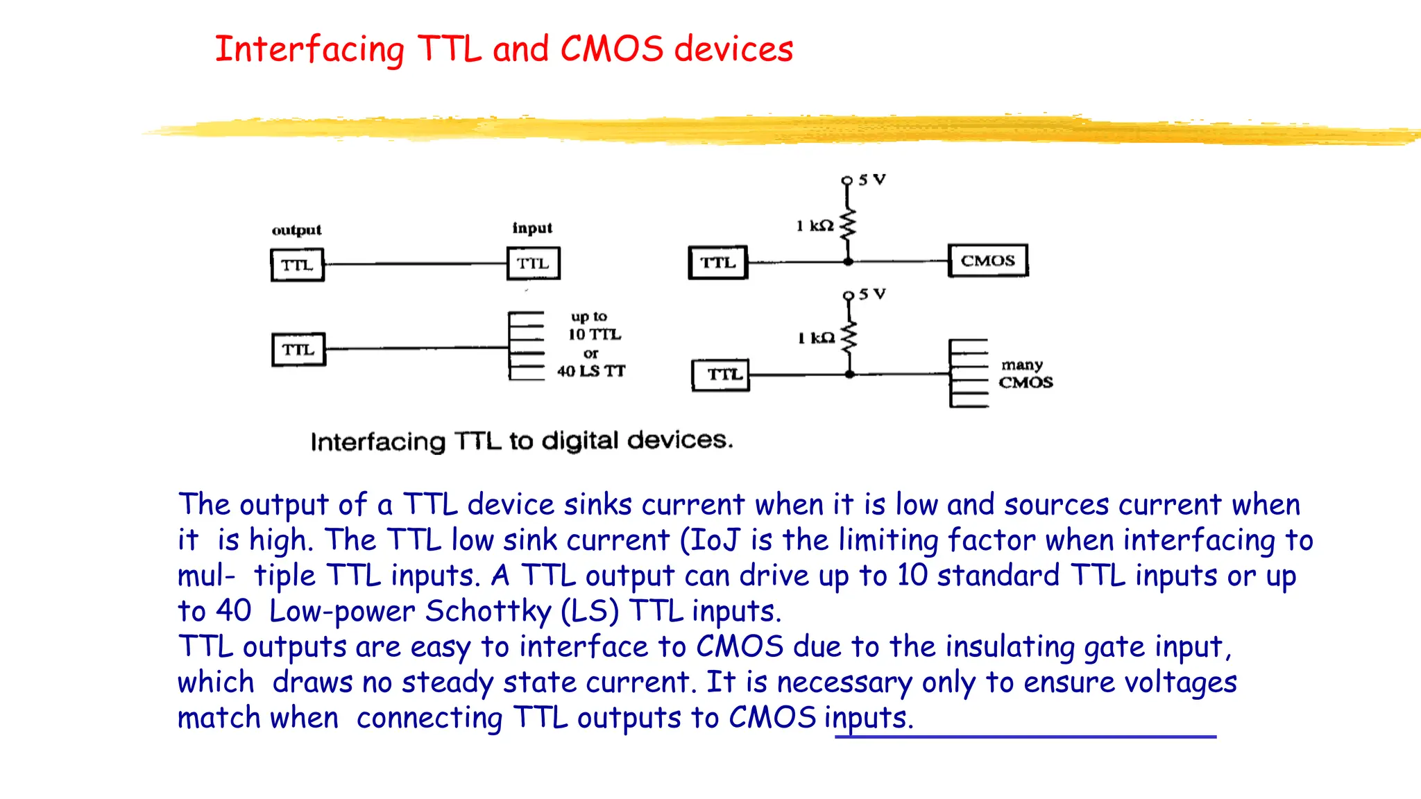
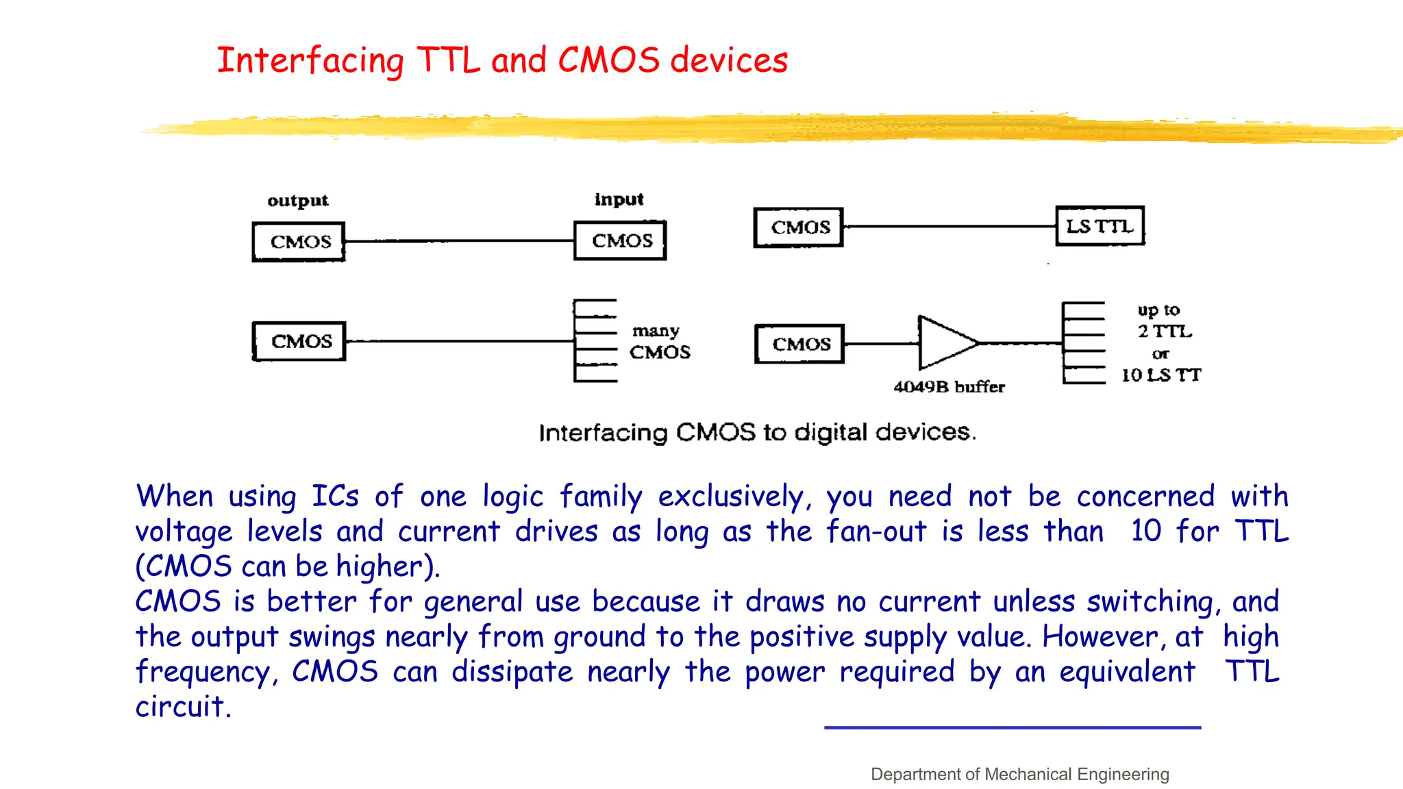
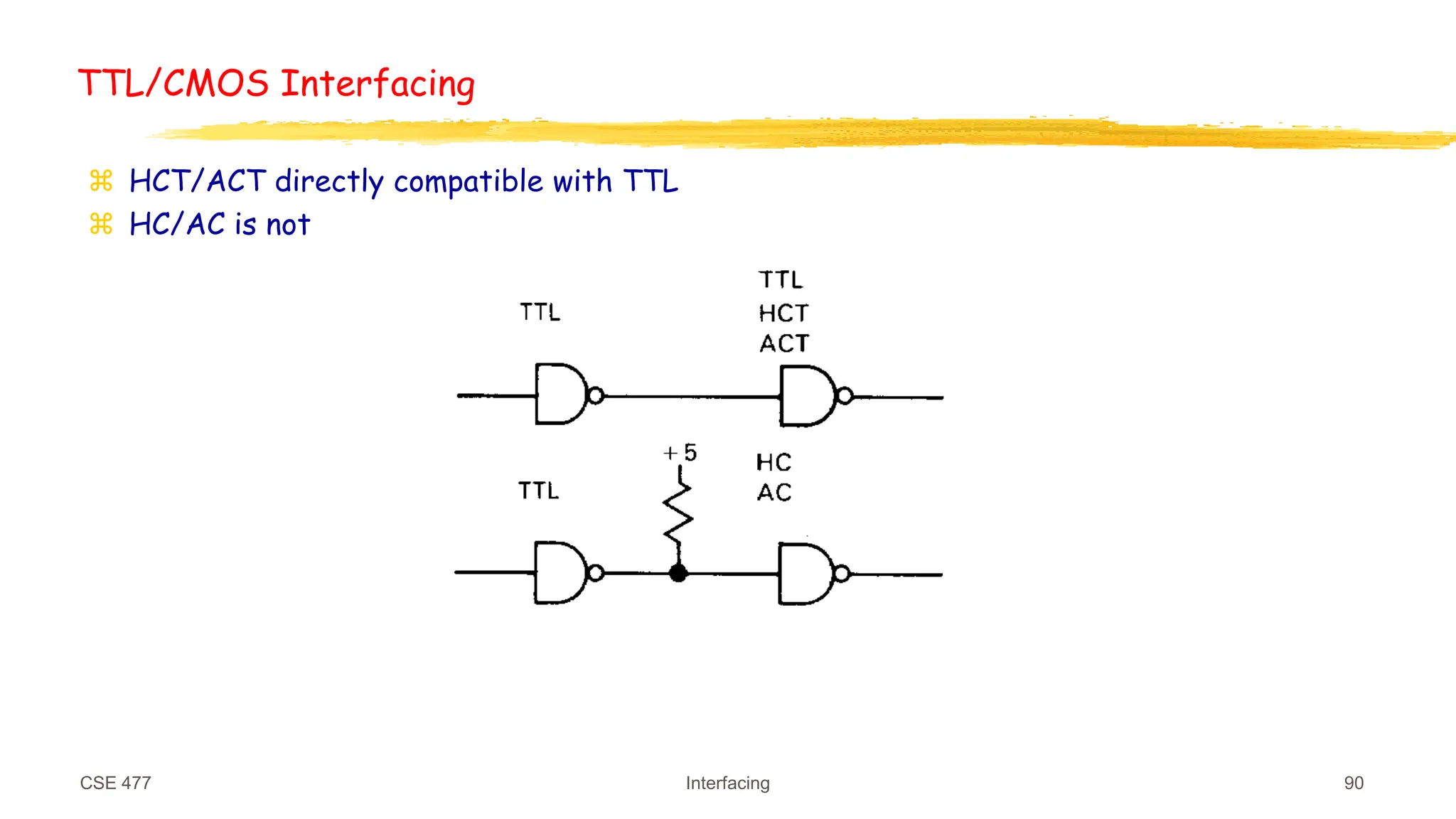
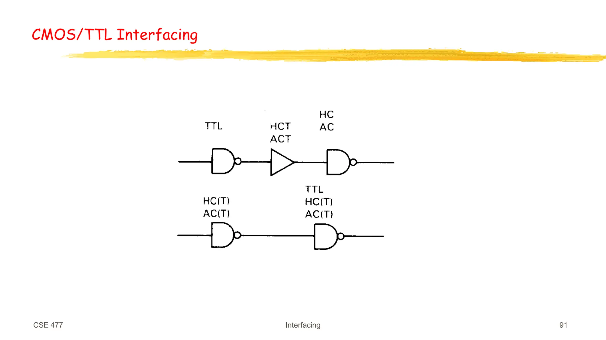
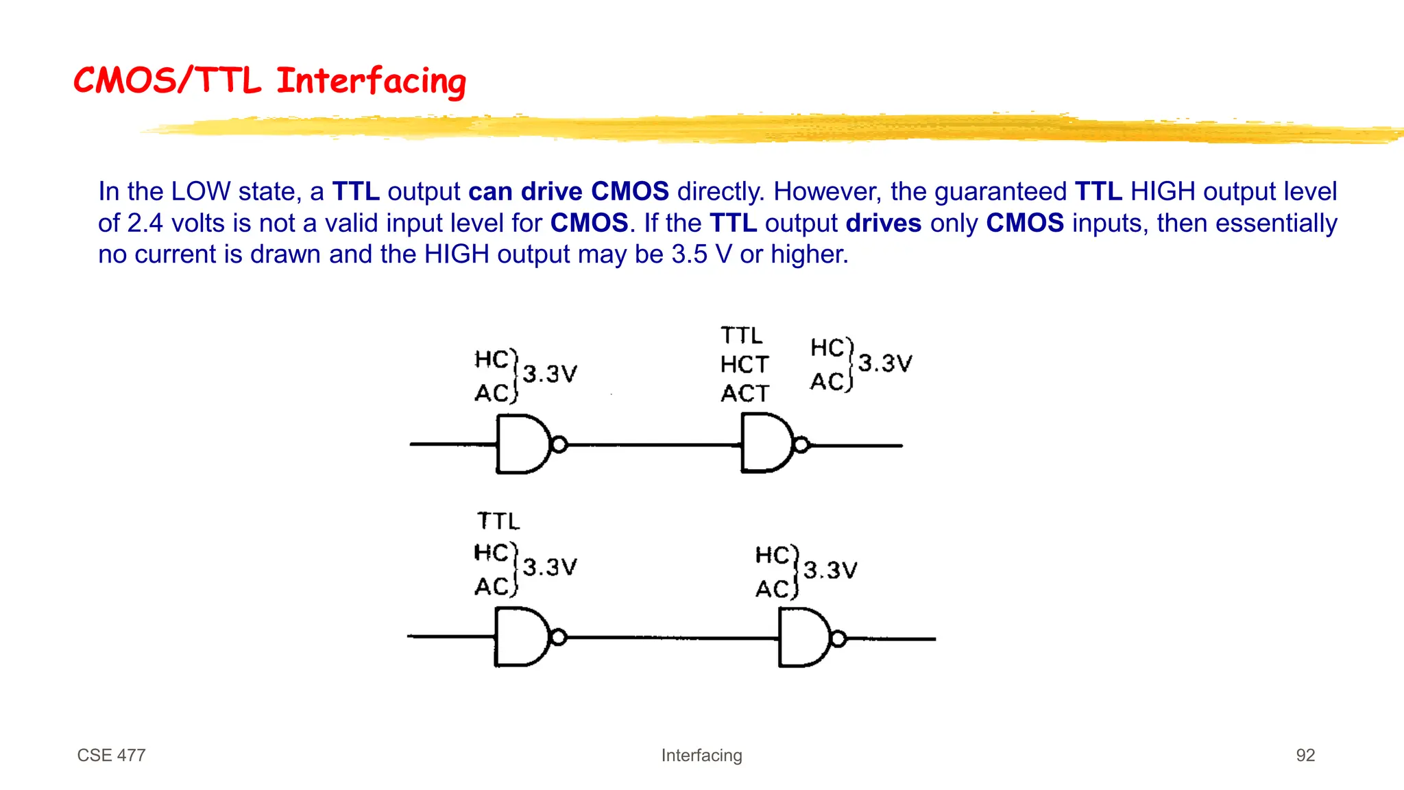
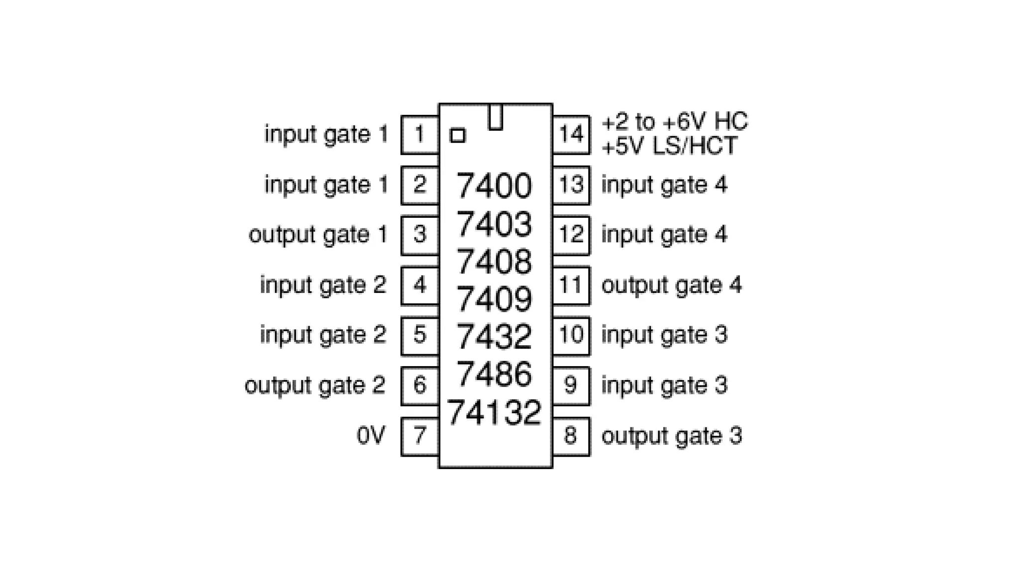
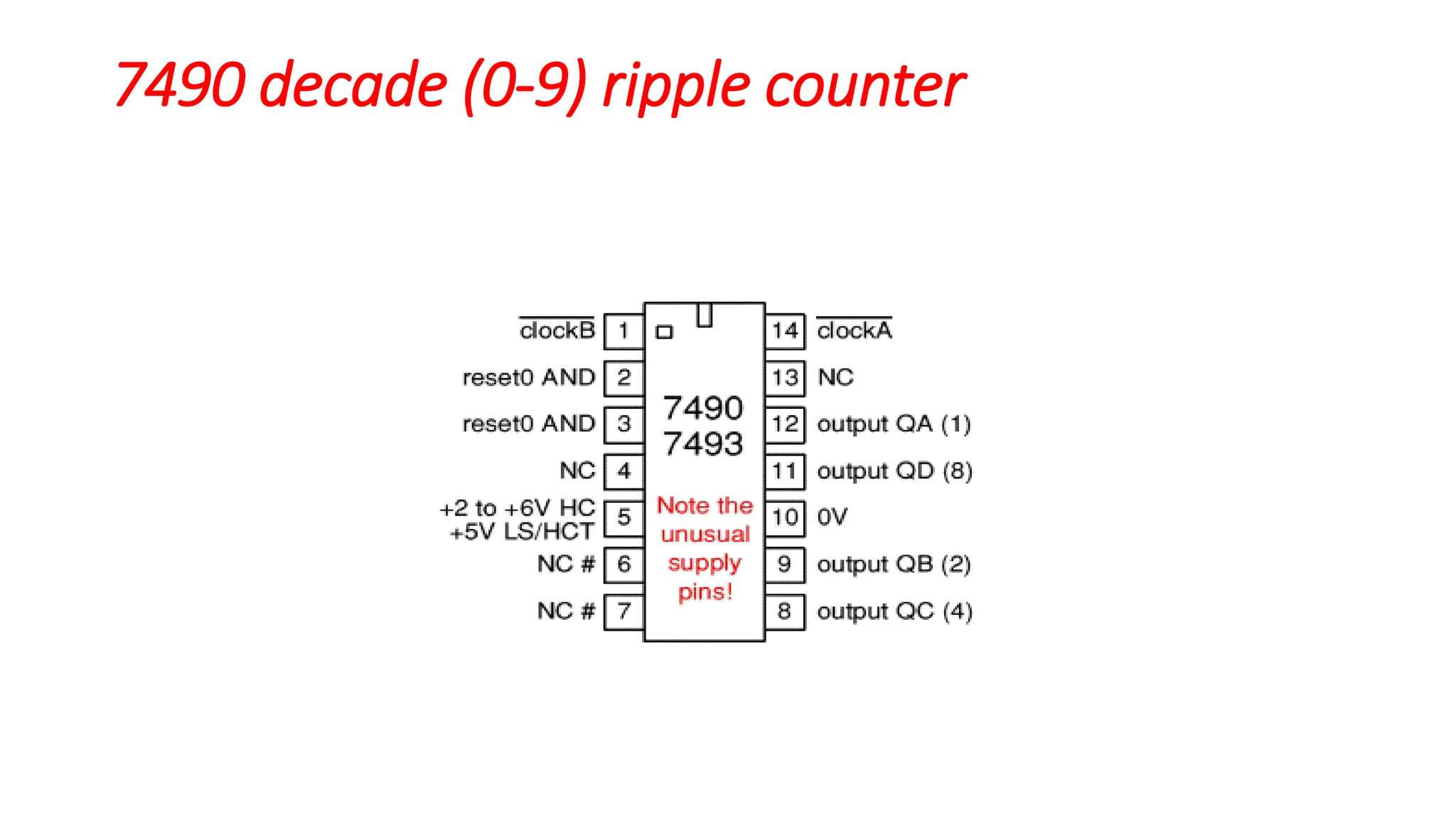
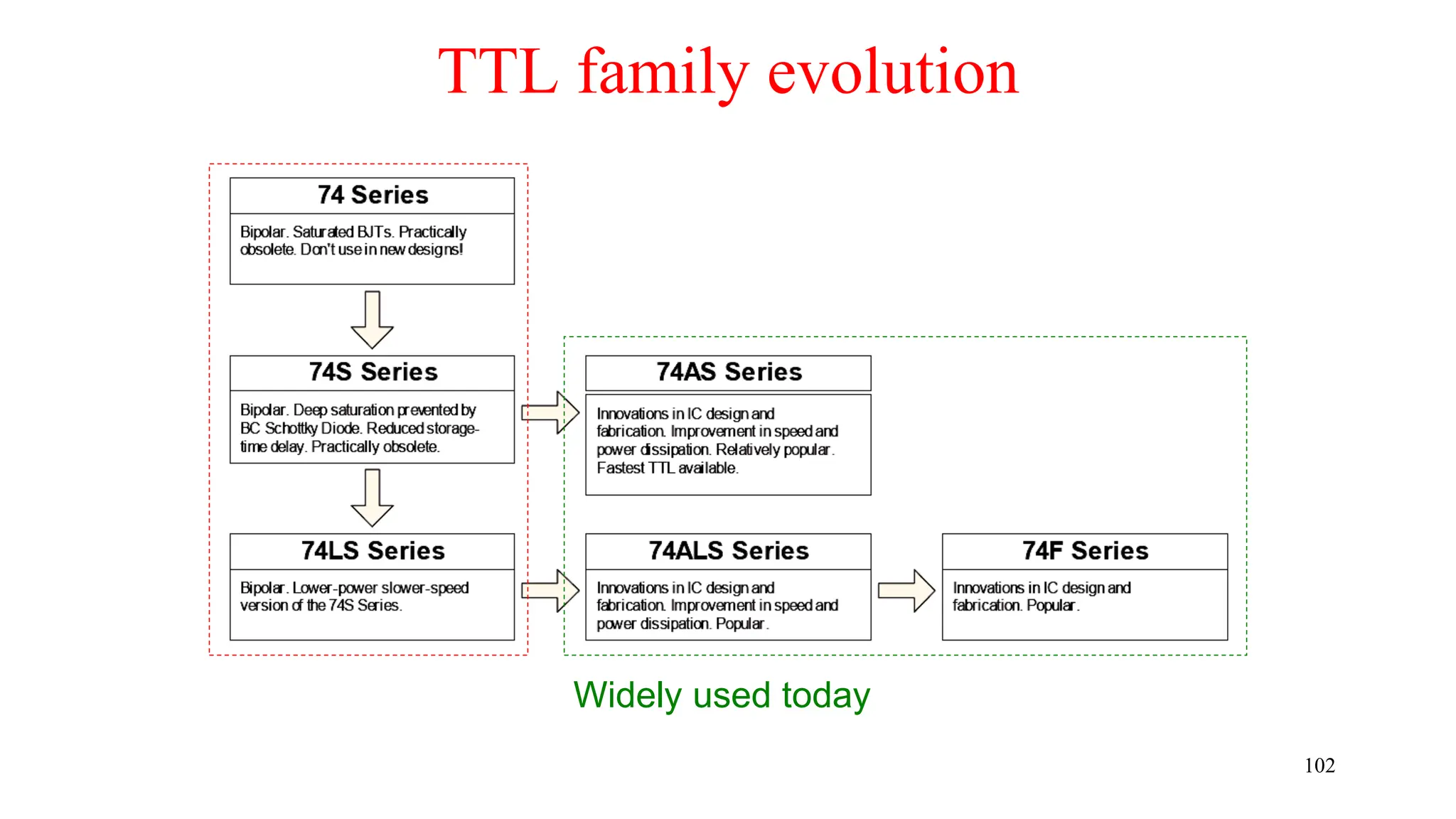
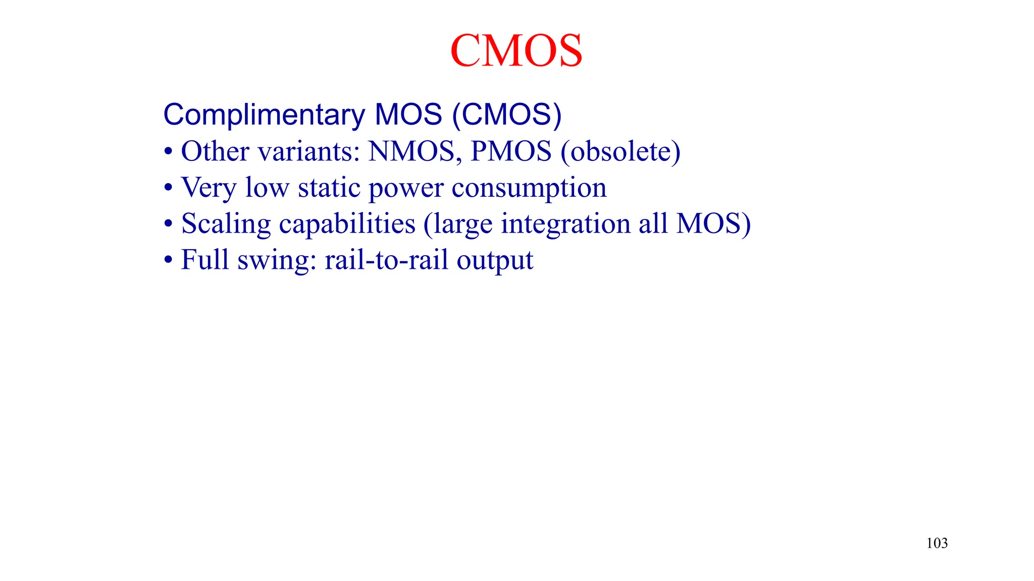
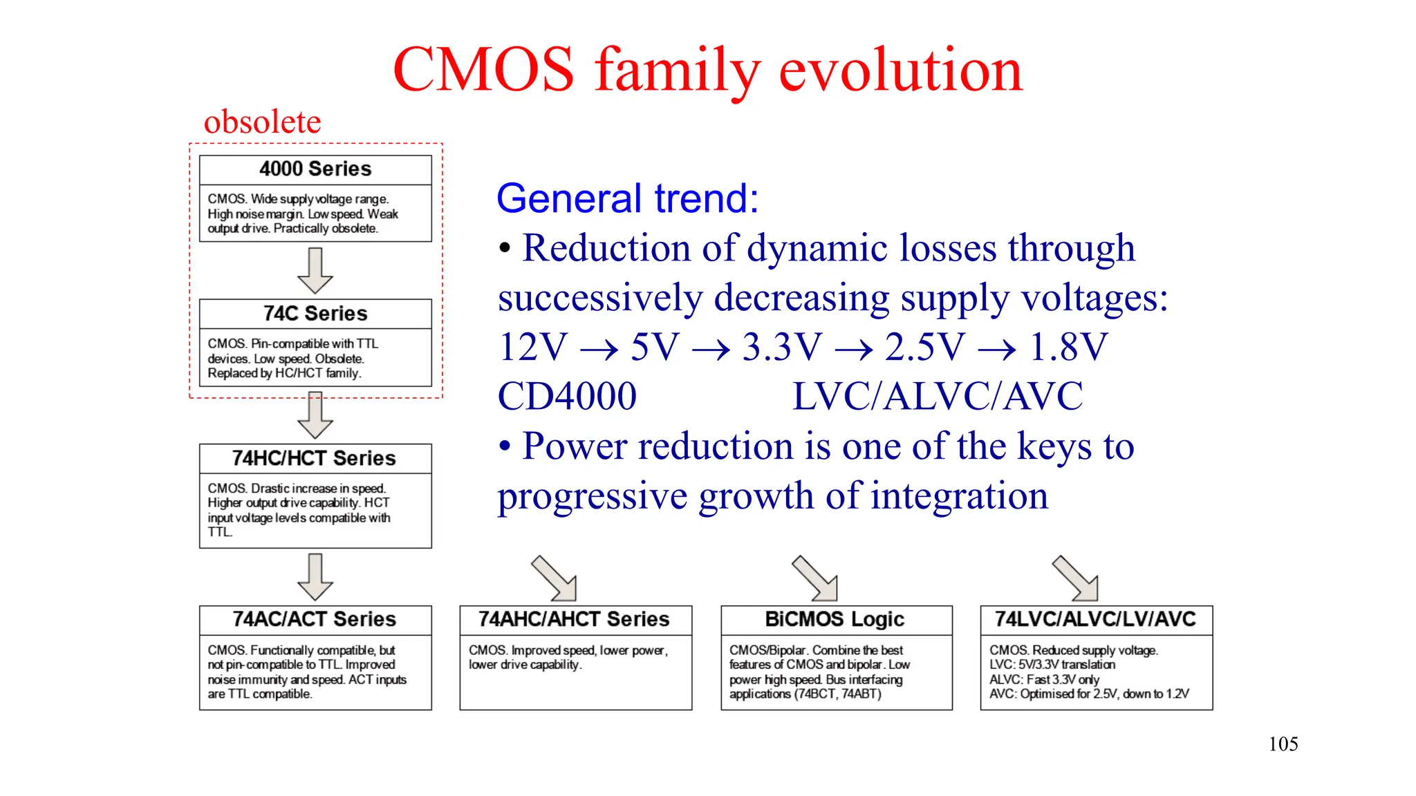
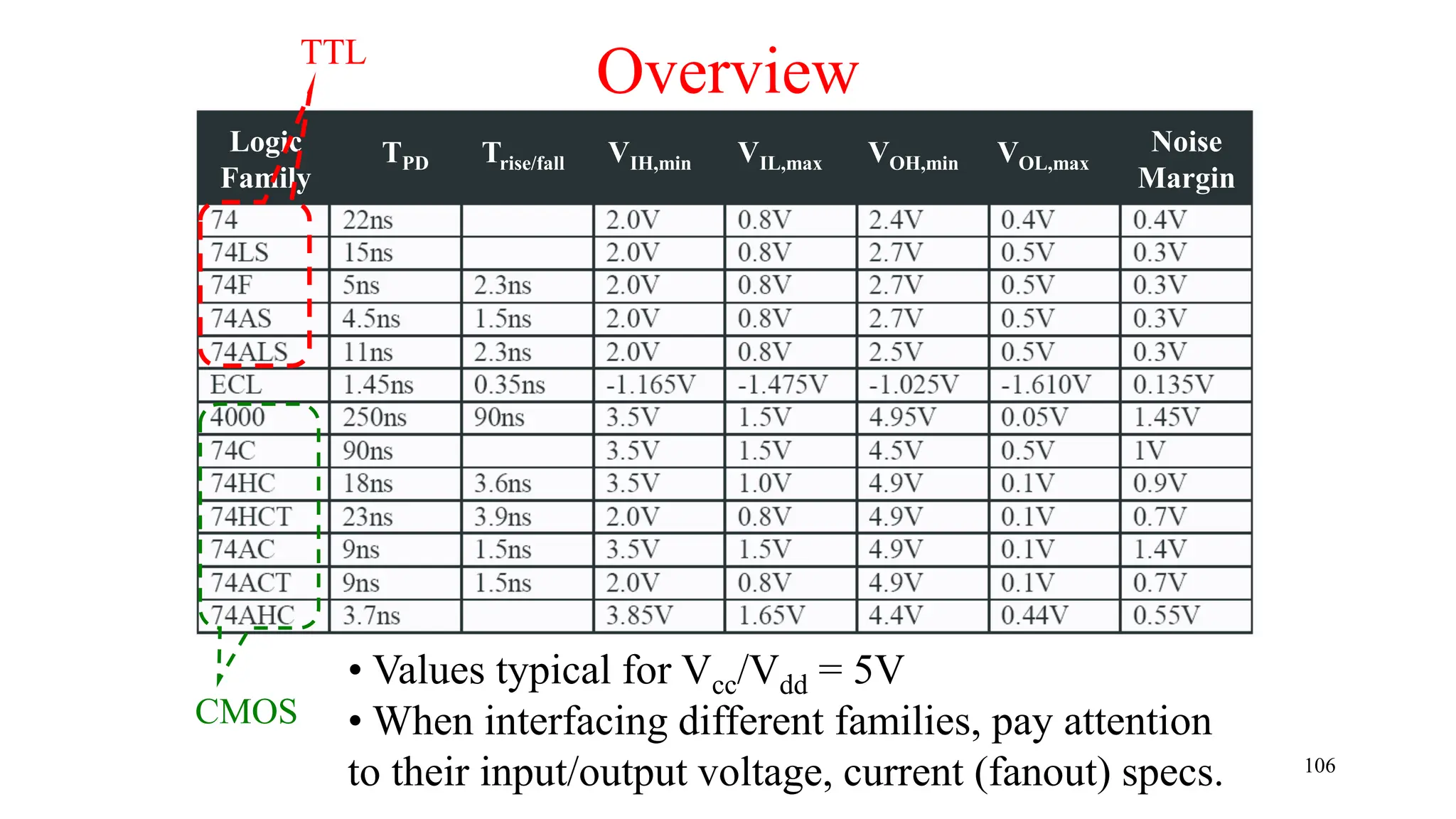
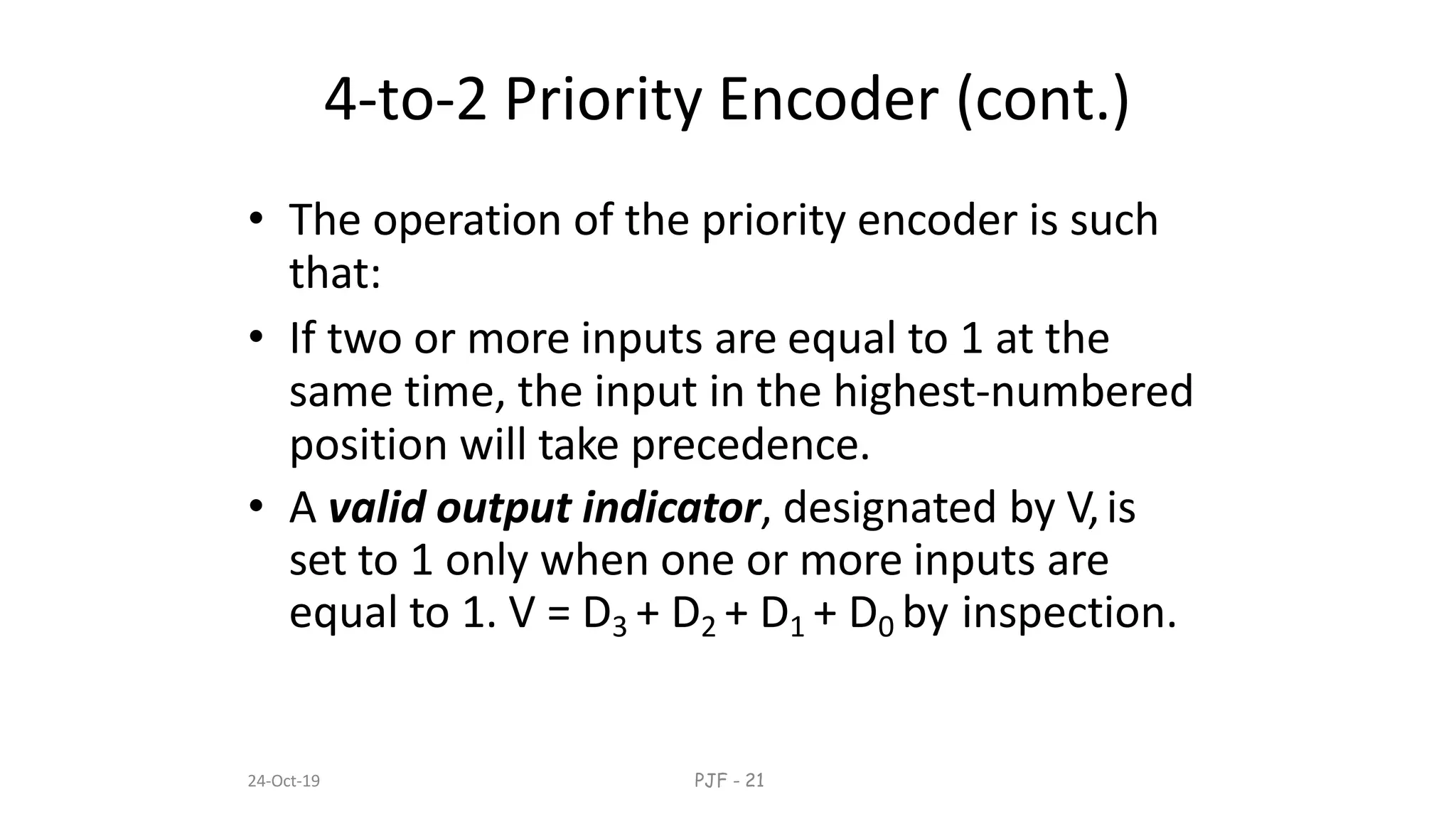
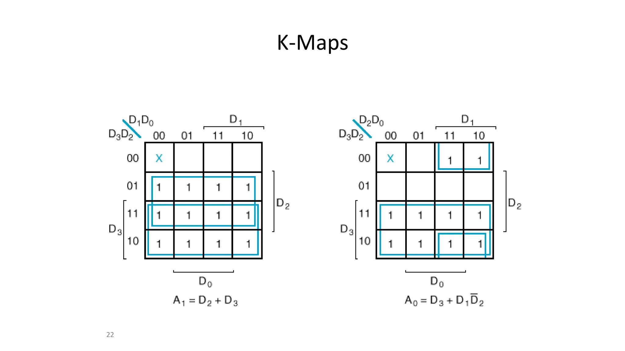
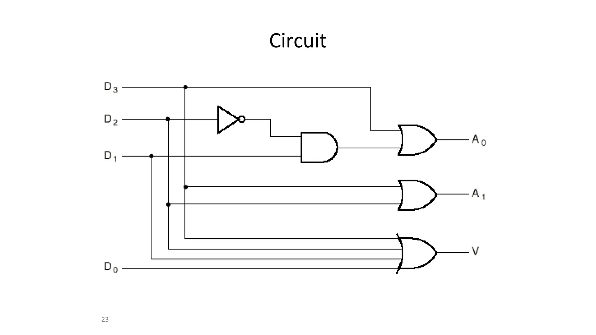
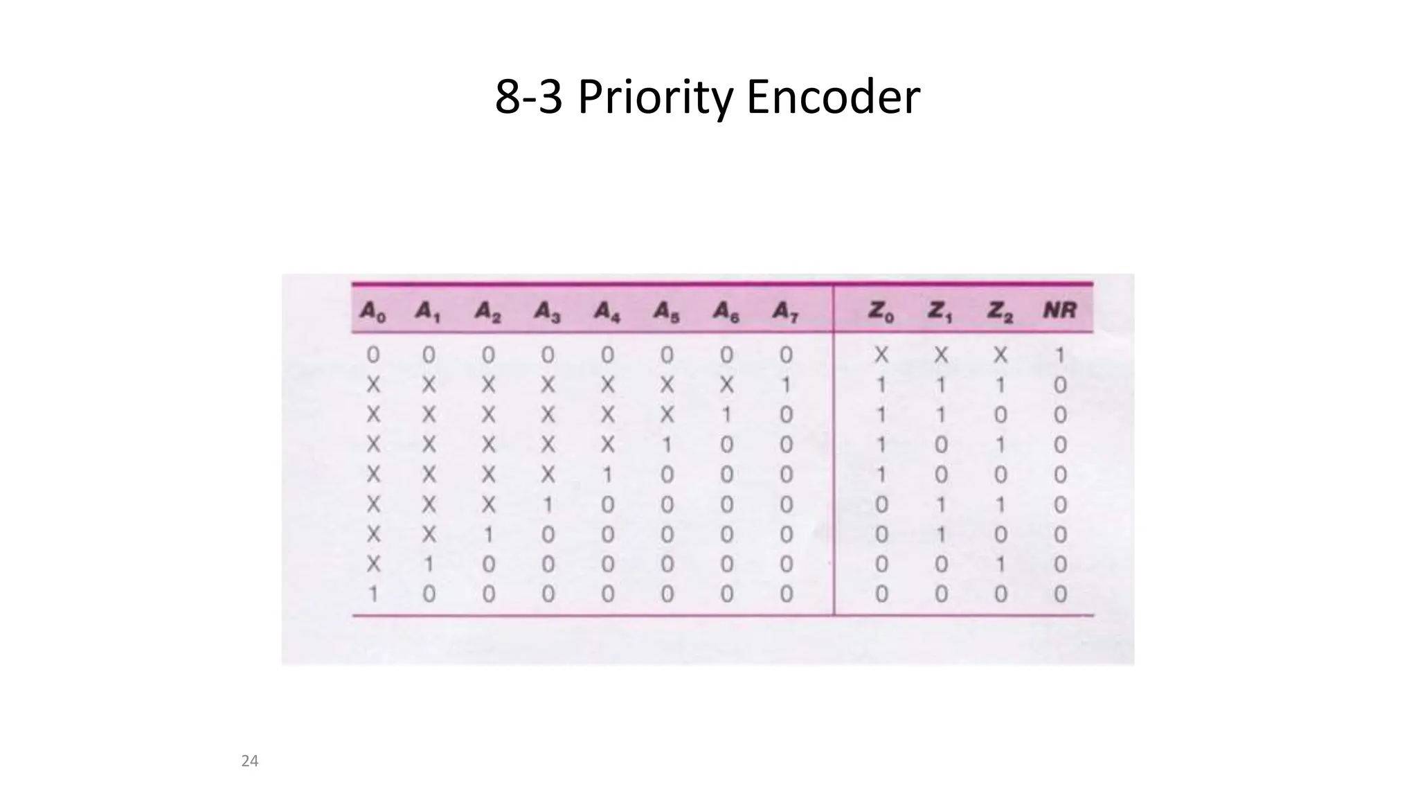
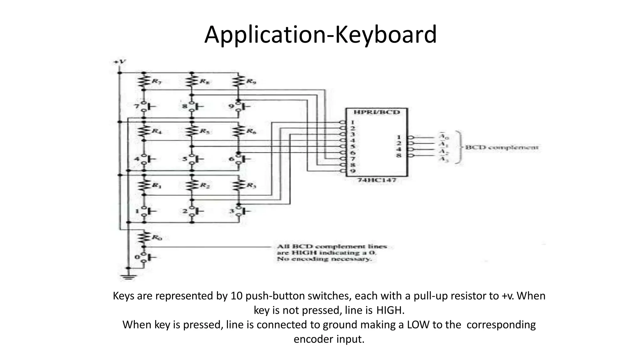
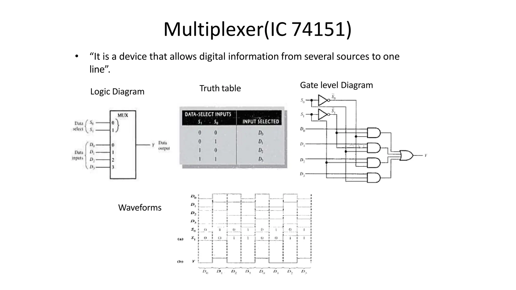
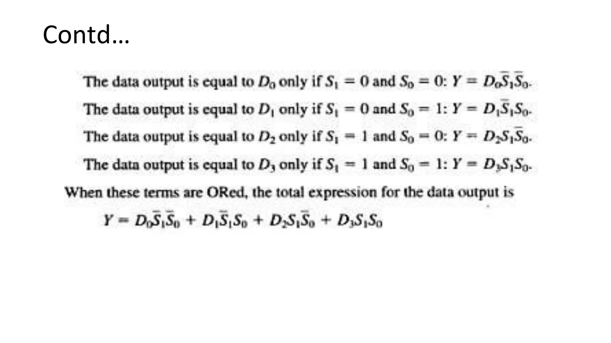
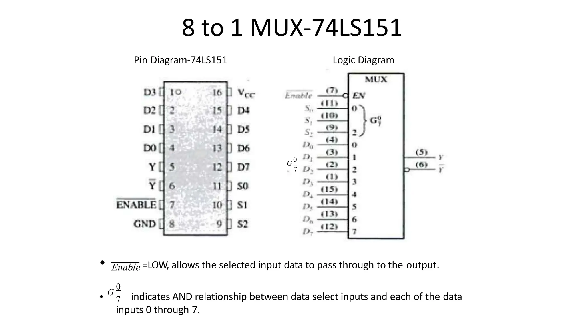
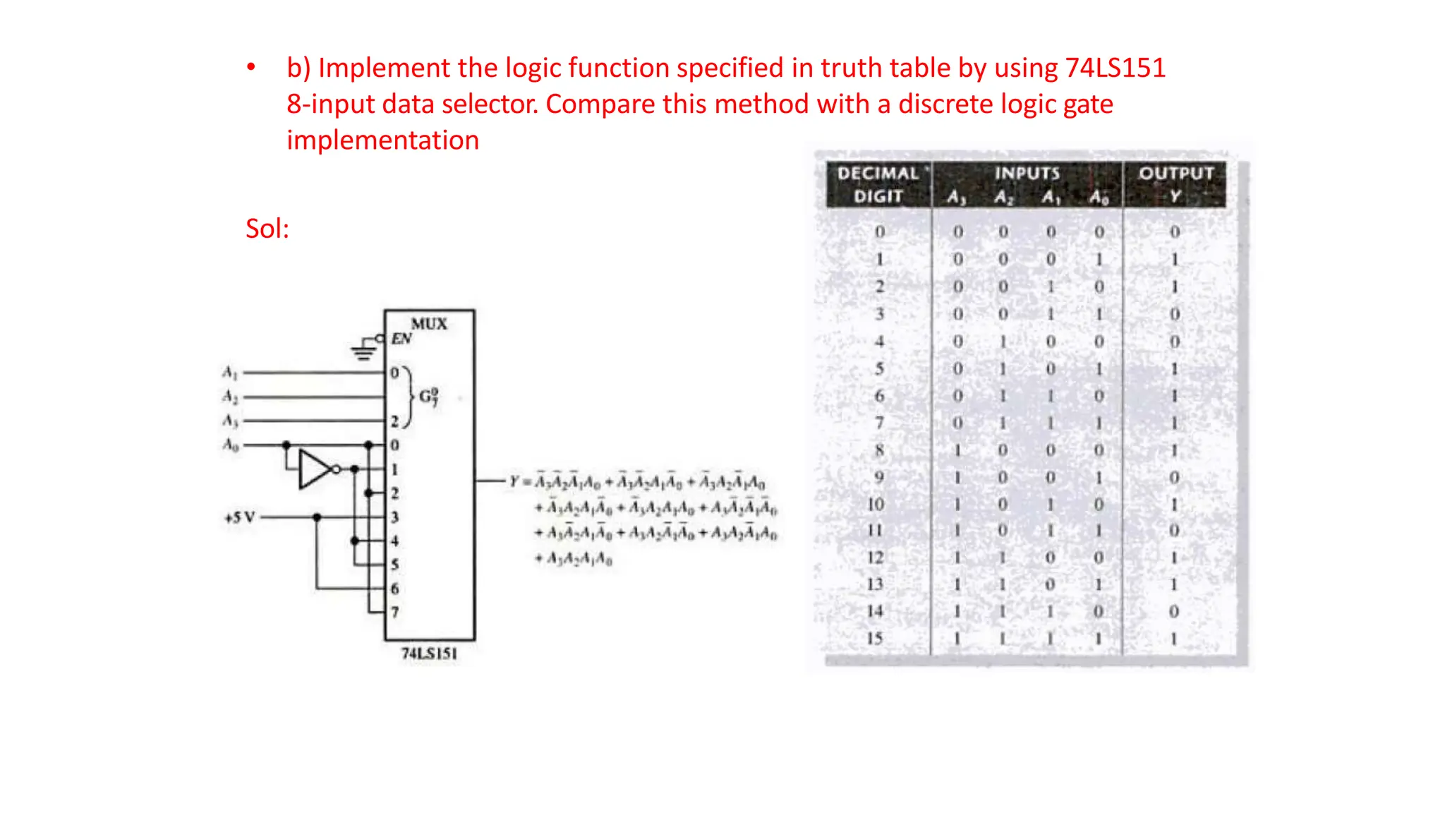
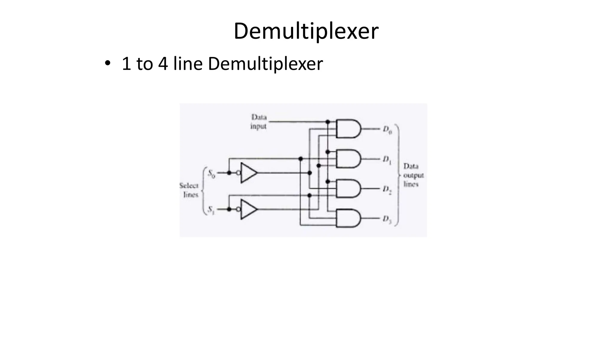
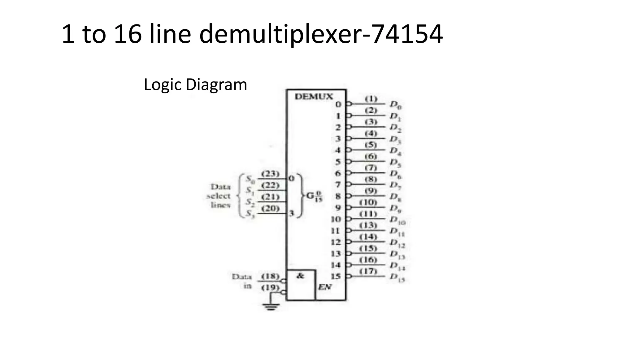
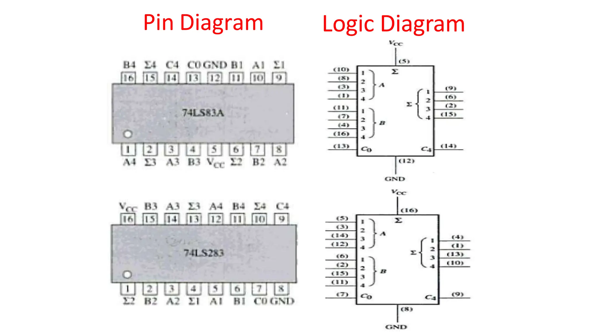
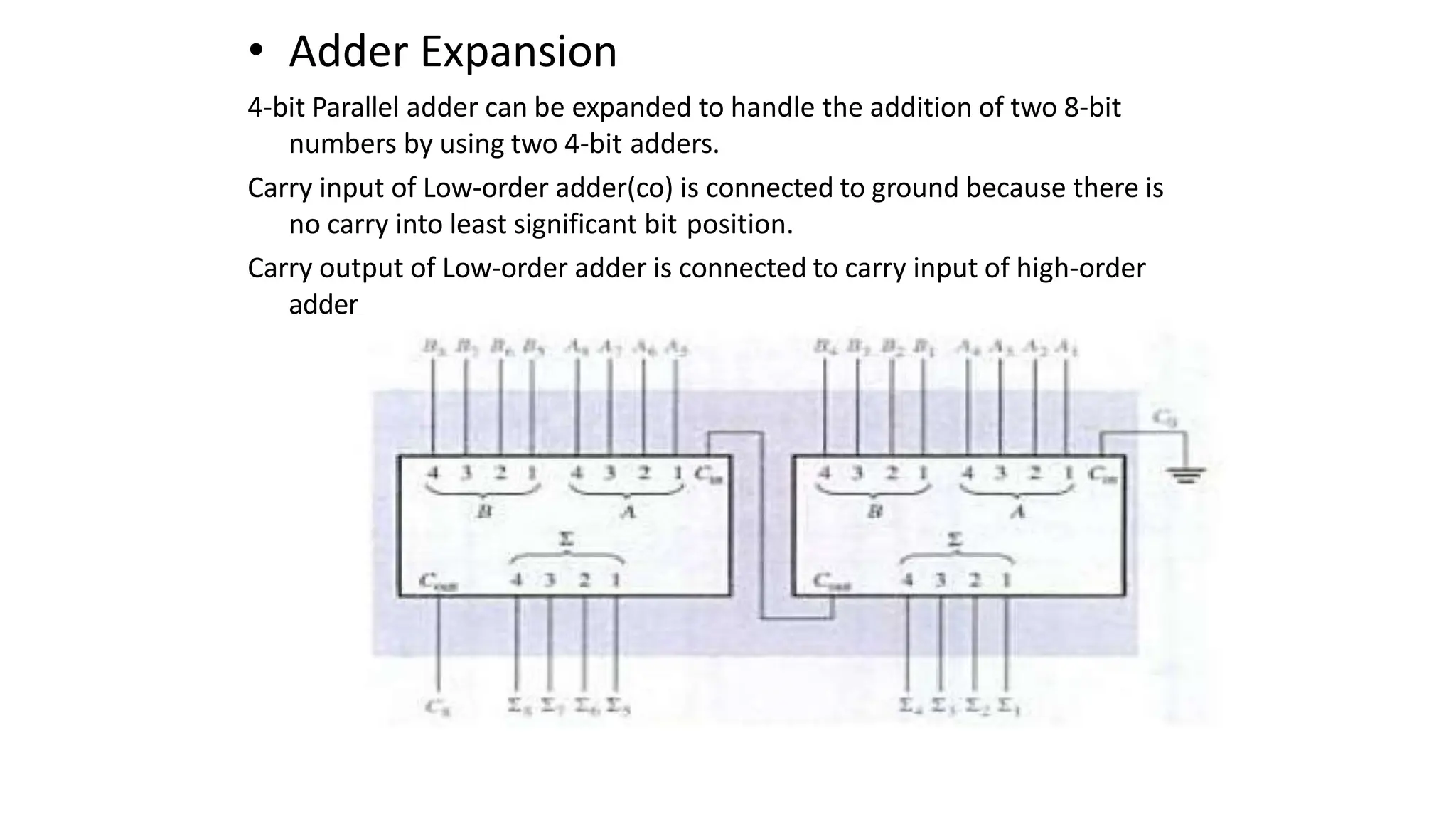
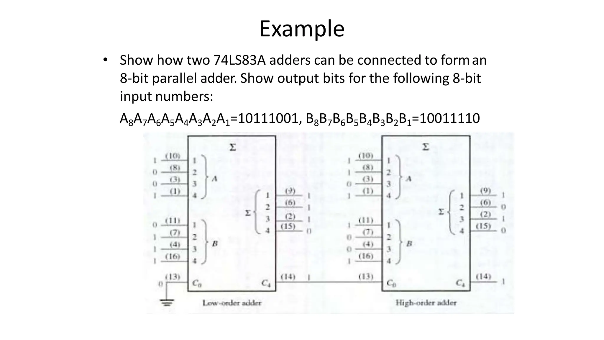
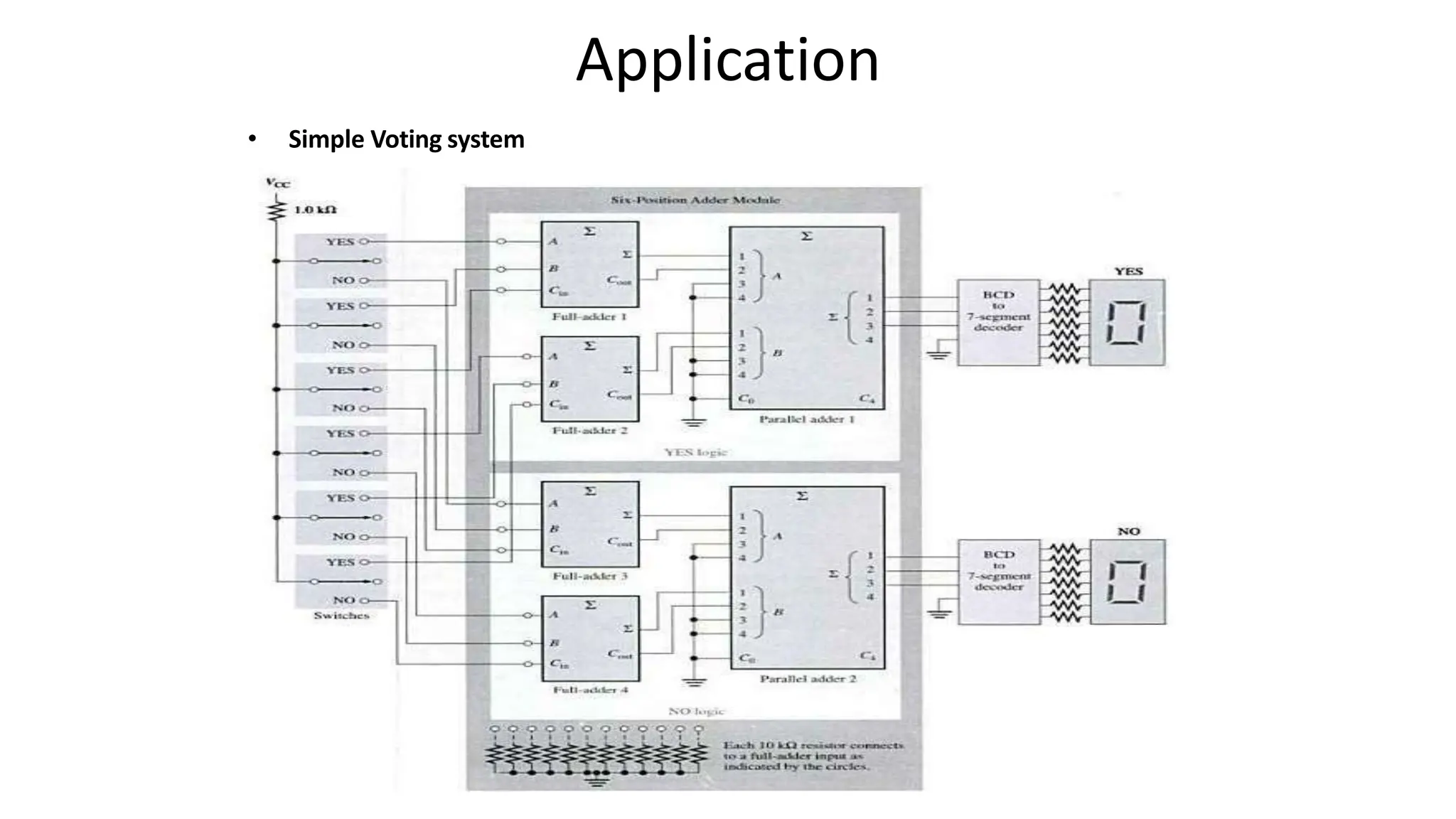
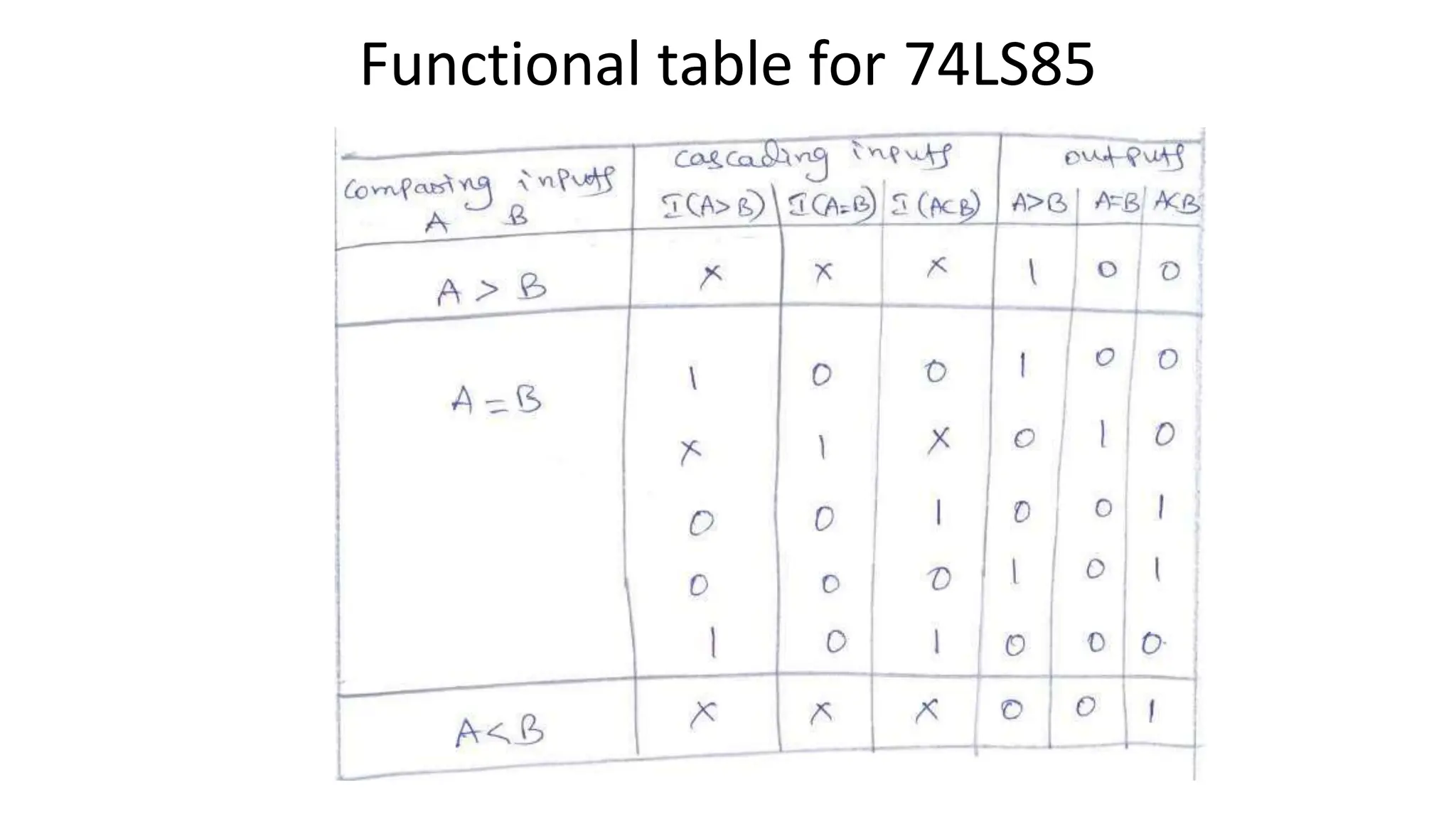
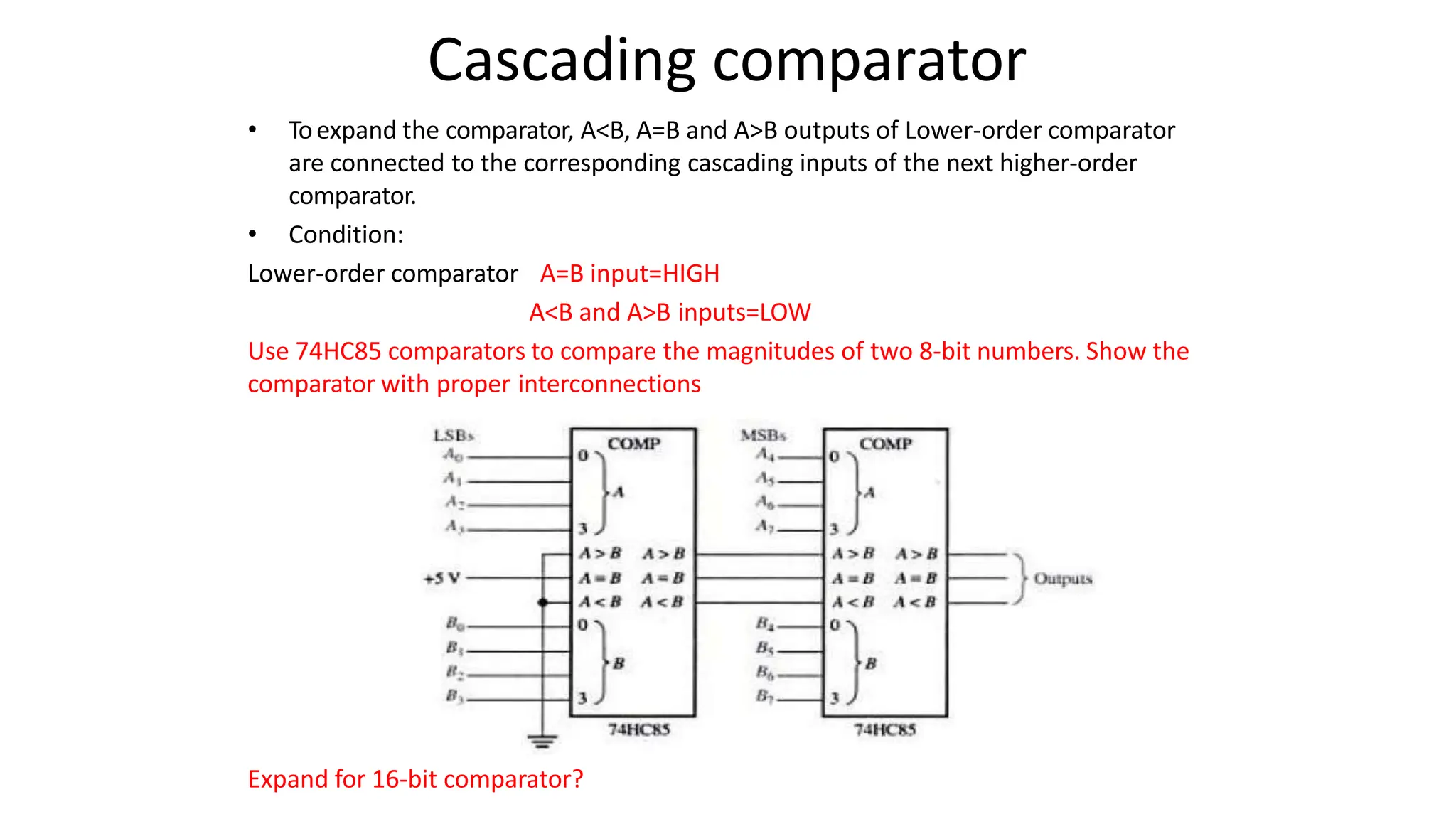
UNIT–IV- Digital Integrated Circuits
Digital Integrated Circuits: Classification of Integrated Circuits,
Comparison of Various Logic Families, CMOS Transmission Gate, IC
interfacing. TTL Driving CMOS & CMOS Driving TTL, Combinational
Logic ICs – Specifications and Applications of TTL-74XX & CMOS 40XX
Series ICs – Code Converters, Decoders, Demultiplexers, LED & LCD
Decoders with Drivers, Encoders, Priority Encoders, Multiplexers,
Demultiplexers, Parity Generators/Checkers, Parallel Binary Adder/
Subtractor, Magnitude Comparators.
Introduction
WHAT IS INTEGRATED CIRCUITS ?
• A complex set of electronic components and their interconnections
that are imprinted onto a tiny slice of semiconducting material.
• Integrated Circuits are usually called ICs or chips.
Integrated circuits were made possible by experimental discoveries
which showed that semiconductor devices could perform the
functions of vacuum tubes and by mid- 20th-century technology
advancements in semiconductor device fabrication.
Contd…
• The integration of large numbers of tiny transistors into a
small chip was an enormous improvement over the manual
assembly of circuits using electronic components.
• The integrated circuit's mass production capability, reliability,
and building-block approach to circuit design ensured the rapid
adoption of standardized ICs in place of designs using discrete
transistors.
Structure of IC
1
• MonolithicIC’s
2
• ThickandThinfilmIC’s
3
• HybridIC’s
Classification of IC
MonolithicIC’s
A Monolithic Microwave Integrated
Circuit, or MMIC is a type of integrated
circuit (IC) device that operates at
microwave frequencies.
devices typically
such as microwave
perform
mixing,
These
functions
power amplification, low-noise
and high-frequency
amplification,
switching.
Inputs and outputs on MMIC devices are frequently matched to a
characteristic impedance of 50 ohms. This makes them easier to use, as
cascading of MMICs does not then require an external matching network.
Thick& ThinFilm IC’s
The general characteristic,
and appearance of thin and
properties,
thick-film
similar, although
integrated
they both
circuits are
differ in many respect from
monolithic integrated circuits.
They are not formed within a semiconductor wafer but on
the surface of an insulating substrate such as glass or an
appropriate ceramic material.
The primary difference between the thin-and-thick-film techniques is
the process employed for the forming the passive component and the
metallic conduction pattern.
The thin-film circuit employs an evaporation or cathode- sputtering
technique; the thick film employs silk-screen techniques.
 A hybrid integrated circuit, HIC, hybrid microcircuit, or simply hybrid is a
miniaturized electronic circuit constructed of individual devices, such as
semiconductor devices (e.g. transistors and diodes) and passive components
(e.g. resistors, inductors, transformers, and capacitors), bonded to a substrate or
printed circuit board (PCB).
HybridIC’s (HIC)
Hybrid circuits are often encapsulated in epoxy, as shown in the photo.
A hybrid circuit serves as a component on a PCB in the same way as a
monolithic integrated circuit.
The difference between the two types of devices is in how they are
constructed and manufactured.
Comparison of Various ICs
Generationsof IC’s
 SSI
 MSI
 LSI
 VLSI
 VVLSI
 WSI
 NANO TECHNOLOGY
Scaleofintegration
SmallScaleIntegration (SSI)
Normally it has about 20 components.
The Minuteman missile and Apollo program needed
lightweight digital computers for their initially-guided flight
computers.
The Apollo guidance computer led and motivated the
integrated-circuit technology, while the Minuteman missile
forced it into mass-production.
MediumScaleIntegration (MSI)
It can have about 100 components.
Medium Scale Integration came in to
industry in late 1960s.
 MSI is the next step in the development of
integrated circuits after 'Small Scale
Integration'.
Medium-Scale Integration allowed more
complex systems to be produced using smaller
circuit boards than in SSI (Small Scale
Integration).
LargeScaleintegration (LSI)
It have about 1000 components.
LSI is the process of integrating or embedding thousands of transistors on
single silicon semiconductor microchip. LSI technology was conceived
in mid-1970s when computer processor microchips were under
development
Very LargeScaleIntegration (VLSI)
Very large scale integration.
It can have about 10,000 components.
VLSI began in the 1970s ,when
complex semiconductor and communication
technologies were being developed.
WaferScaleIntegration(WSI)
The evolution in semiconductor technology that builds a gigantic circuit on an
entire wafer.
Just as the integrated circuit eliminated cutting apart thousands of transistors from
the wafer only to wire them back again on circuit boards, wafer scale integration
eliminates cutting apart the chips.
Advantages of Integrate Circuit
• It is quite small in size practically around 20,000 electronic components can
be incorporated in a single square inch of IC chip.
• Many complex circuits are fabricated in a single chip and hence this
simplifies the designing of a complex electronic circuit. Also it improves the
performance.
• Reliability of ICs is high
• These are available at low cost due to bulk production.
• ICs consume very tiny power.
• Higher operating speed due to absence of parasitic capacitance effect.
• Very easily replaceable from the mother circuit.
Disadvantages of Integrate Circuit or IC
• IC is unable to dissipate heat in required rate when current in it
increased. That is why ICs are often damaged due to over current
flowing through them.
• Inductors and Transformers cannot be incorporated in ICs.
IC’sPackages
SingleInline
Packaging
DualInline
Packaging
ZigzagInline
packaging
SingleInlinePackaging (SIP)
A single in-line (pin) package (SIP or SIPP) has
one row of connecting pins. It is not as popular as
the DIP, but has been used for
packaging RAM chips and multiple resistors with
a common pin. SIPs group RAM chips together on
a small board either by the DIP process or surface
mounting SMD process.
DualInlinePackaging (DIP)
A dual in-line package is an electronic component
package with a rectangular housing and two parallel
rows of electrical connecting pins. The package
may be through-hole mounted to a printed circuit
board or inserted in a socket.
Zigzag InlinePackaging
The zigzag in-line package or ZIP was a short-lived
packaging technology for integrated circuits,
particularly dynamic RAM chips.
A ZIP is an integrated circuit encapsulated in a slab of
plastic with 20 or 40 pins, measuring (for the ZIP-20
package) about 3 mm x 30 mm x 10 mm.
The package's pins protrude in two rows from one of
the long edges. The two rows are staggered by 1.27 mm
(0.05"), giving them a zigzag appearance, and allowing
them to be spaced more closely than a rectangular grid
would allow
Zigzag InlinePackaging
Logic Family
• Logic Families indicate the type of logic circuit used in the IC.
• A Circuit configuration or arrangement of the circuit elements in a
special manner will result in a particular Logic Family.
• The set of digital ICs belonging to the same logic family are
electrically compatible with each other
29
Logic Families
Logic Family : A collection of different IC’s that have similar
circuit characteristics
The circuit design of the basic gate of each logic family is the same
The most important parameters for evaluating and comparing logic
families include :
Logic Levels
Power Dissipation
Propagation delay
Noise margin
Fan-out ( loading )
30
Example Logic Families
General comparison or three commonly available logic
families.
the most important to understand
31
Implementing Logic Circuits
There are several varieties of transistors – the
building blocks of logic gates – the most important
are:
BJT (bipolar junction transistors)
one of the first to be invented
FET (field effect transistors)
especially Metal-Oxide Semiconductor types (MOSFET’s)
MOSFET’s are of two types: NMOS and PMOS
32
Transistor Size Scaling
Performance improves as size is decreased: shorter switching time, lower power consumption.
2 orders of magnitude reduction in transistor size in 30 years.
33
Moore’s Law
In 1965, Gordon Moore predicted that the number of transistors that can
be integrated on a die would double every 18 to 24 months
i.e., grow exponentially with time
Considered a visionary – million transistor/chip barrier was crossed in
the 1980’s
2300 transistors, 1 MHz clock (Intel 4004/4040) - 1971
42 Million transistors, 2 GHz clock (Intel P4) - 2001
140 Million transistors, (HP PA-8500)
34
Moore’s Law and Intel
From Intel’s 4040 (2300 transistors) to Pentium II (7,500,000 transistors) and beyond
35
TTL and CMOS
Connecting BJT’s together gives rise to a family of logic gates
known as TTL
Connecting NMOS and PMOS transistors together gives rise
to the CMOS family of logic gates
BJT
MOSFET
(NMOS, PMOS)
TTL CMOS
transistor types
logic gate families
36
Electrical Parameters And
Interpretation Of Data Sheets
Voltages and Currents
Noise Margin
Power Dissipation
Propagation Delay
Speed-Power Product
Fan-In, Fan-Out
Comparison of Logic Families
Interpretation of Data Sheets
37
Electrical Characteristics
TTL
faster (some versions)
strong drive capability
rugged
CMOS
lower power consumption
simpler to make
greater packing density
better noise immunity
• Complex IC’s contain many millions of transistors
• If constructed entirely from TTL type gates would melt
• A combination of technologies (families) may be used
• CMOS has become most popular and has had greatest development
38
For a Low-state gate driving a second gate, we
define:
VOL (max), low-level output voltage, the maximum voltage level
that a logic gate will produce as a logic 0 output.
VIL (max), low-level input voltage, the maximum voltage level
that a logic gate will recognize as a logic 0 input. Voltage above
this value will not be accepted as low.
IOL , low-level output current, current that flows from an output
in the logic 0 state under specified load conditions.
IIL , low-level input current, current that flows into an input when
a logic 0 voltage is applied to that input.
Voltage & Current
Inputs are
connected to Vcc
instead of
Ground
Ground
V IL
VOL
I OL I IL
39
Electrical Characteristics
Important characteristics are:
VOHmin min value of output recognized as a ‘1’
VIHmin min value input recognized as a ‘1’
VILmax max value of input recognized as a ‘0’
VOLmax max value of output recognized as a ‘0’
Values outside the given range are not allowed.
logic 0
logic 1
indeterminate
input voltage
40
Typical acceptable voltage ranges for positive logic 1 and
logic 0 are shown below
A logic gate with an input at a voltage level within the
‘indeterminate’ range will produce an unpredictable output
level.
Logic Level & Voltage Range
Logic 1
Logic 0
5.0V
0V
2.5V
Indeterminate
0.8V
TTL
Logic 1
Logic 0
5.0V
Indeterminate
0V
1.5V
CMOS
3.5V
41
Noise Margin
If noise in the circuit is high enough
it can push a logic 0 up or drop a
logic 1 down into the indeterminate
or “illegal” region
The magnitude of the voltage
required to reach this level is the
noise margin
Noise margin for logic high is:
NMH = VOHmin – VIHmin
VOHmin
VIHmin
VILmax
VOLmax
logic 0
logic 1
indeterminate
input voltage
42
Noise Margin
Difference between the worst case output voltage of one stage and worst
case input voltage of next stage
Greater the difference, the more unwanted signal that can be added
without causing incorrect gate operation
NMhigh = VOHmin - VIHmin
NMlow = VILmax - VOLmax
43
Given the following parameters, calculate the
noise margin of 74LS series.
Parameter 74LS
VIH(min) 2V
VIL(max) 0.8V
VOH (min) 2.7V
VOL(max) 0.4V
Solution:
High Level Noise Margin, VNH = VOH (min) - VIH (min)=2.7V-2.0V=0.7V
Low Level Noise Margin, VNL = VIL (max) - VOL (max)=0.8V-0.4V=0.4V
Worked Example
44
Noise immunity of a logic circuit refers to the circuit’s ability
to tolerate noise voltages on its inputs.
A quantitative measure of noise immunity is called noise
margin
High Level Noise Margin, VNH = VOH (min) - VIH (min)
Low Level Noise Margin, VNL = VIL (max) - VOL (max)
Noise Margin & Noise Immunity
Logic 1
Logic 0
Logic 0
Logic 1
VOH (min)
VOL (max)
VIH (min)
VIL (max)
VNH
VNL
Output Voltage Ranges Input Voltage Ranges
45
Further Important Characteristics
The propagation delay (tpd) which is the time
taken for a change at the input to appear at the
output
The fan-out, which is the maximum number of
inputs that can be driven successfully to either
logic level before the output becomes invalid
46
Speed: Rise & Fall Times
Rise Time
Time from 10% to 90% of signal, Low to High
Fall Time
Time from 90% to 10% of signal, High to Low
rise time
10% 90% 90% 10%
fall time
47
A logic gate always takes some time to change states
tPLH is the delay time before output changes from low to high
tPHL is the delay time before output changes from high to low
both tPLH & tPHL are measured between the 50% points on the
input and output transitions
Speed: Propagation Delay
50%
Input
Output
0
0
tPHL tPLH
48
Power Dissipation
Static
I2R losses due to passive components, no input signal
Dynamic
I2R losses due to charging and discharging capacitances through resistances, due
to input signal
49
Speed (propagation delay) and power consumption
are the two most important performance parameters
of a digital IC.
A simple means for measuring and comparing the
overall performance of an IC family is the speed-
power product (the smaller, the better).
For example, an IC has
an average propagation delay of 10 ns
an average power dissipation of 5 mW
the speed-power product = (10 ns) x (5 mW)
= 50 picoJoules (pJ)
Speed-Power Product
50
Logic Family Tradeoffs
Looking for the best
speed/power product
tp and Pd are normally
included in the data
sheet for each device
Older logic families
are the worst
CMOS is one of the
best
FPGAs use CMOS
51
Comparison of Logic Families
52
TTL - Example SN74LS00
Recommended operating conditions
Vcc supply voltage 5V ± 0.5 V
input voltages VIH = 2V
VIL = 0.8V
Electrical Characteristics
output voltage VOH = 2.7V
(worst case) VOL = 0.5V
max input currents IIH = 20µA
IIL = -0.4mA
propagation delay tpd = 15 nS
noise margins for a logic 0 = 0.3V
for a logic 1 = 0.7V
Fan-out 20 TTL loads
5 Volt
0 Volt
0.8
0.5
2.0
2.7
Input
Range
for 1
Input
Range
for 0
Output
Range
for 0
Output
Range
for 1
53
Fan-In
Number of input signals to a gate
Not an electrical property
Function of the manufacturing process
NAND gate with a
Fan-in of 8
54
Fan-Out
A measure of the ability of the output of one gate to
drive the input(s) of subsequent gates
Usually specified as standard loads within a single
family
e.g., an input to an inverter in the same family
May have to compute based on current drive
requirements when mixing families
Although mixing families is not usually recommended
55
VOH
IIH
Low
VOL
IIL
High
Current Sourcing and Sinking
Current-source : the driving gate produces a
outgoing current
Current-sinking : the driving gate receives an
incoming current
56
Fan-Out
An illustration of fan-out and the associated source
and sink currents
57
SSI Devices
Each package contains a code identifying the package
N74LS00
Manufacturers Code
N = National Semiconductors
SN = Signetics
Specification
Family
L
LS
H
Member
00 = Quad 2 input NAND
02 = Quad 2 input Nor
04 = Hex Invertors
20 = Dual 4 Input NAND
58
7400 Series History
1960s space program drove
development of 7400 series
Consumed all available devices for
internal flight computer
$1000 / device (1960 dollars)
10:1 integration improvement over
discrete transistors
1963 Minuteman missile forced
7400 into mass production
Drove pricing down to $25 / circuit
(1963 dollars)
59
7400 Series Evolution
BJT storage time reduction by using a BC Schottky diode.
Schottky diode has a Vfw=0.25V. When BC junction becomes forward
biased Schottky diode will bypass base current.
B
C
60
Characteristics: TTL and MOS
TTL stands for Transistor-Transistor Logic
uses BJTs
MOS stands for Metal Oxide Semiconductor
uses FETs
MOS can be classified into three sub-families:
PMOS (P-channel)
NMOS (N-channel)
CMOS (Complementary MOS, most common)
Remember:
61
A
B Y O/P
+Vcc
Q
1
Q 2
Q
3
Q
4
4K 1.6K 130
R1 R2
R3
R4
1K
I CQ1
D 3
D
1 D2
A B ICQ1 Q1 Q2 Q3 Q4 Y O/P
0 0 + ON OFF OFF ON 1
0 1 + ON OFF OFF ON 1
1 0 + ON OFF OFF ON 1
1 1 - OFF ON ON OFF 0
A standard TTL NAND gate circuit
Table explaining the operation of the
TTL NAND gate circuit
TTL Circuit Operation
62
Transistor-Transistor Logic Families
Transistor-Transistor Logic Families:
74L Low power
74H High speed
74S Schottky
74LS Low power Schottky
74AS Advanced Schottky
74ALS Advance Low power Schottky
63
+VDD
O/P
I/P
S
D
D
S
Q
Q
1
2
I/P Q1 Q2 O/P
0 ON OFF 1
1 OFF ON 0
Table explaining the operation of
the CMOS inverter circuit
A CMOS inverter circuit
MOS Circuit Operation
64
CMOS Logic Families
CMOS Logic Families
40xx/45xx Metal-gate CMOS
74C TTL-compatible CMOS
74HC High speed CMOS
74ACT Advanced CMOS -TTL compatible
65
CMOS Family Evolution
CMOS Logic Trend: Reduction of dynamic losses
(cross-conduction, capacitive charge/discharge cycles)
by decreasing supply voltages:
12V→5V →3.3V →2.5V → 1.8V → 1.5V …
Reduction of IC power dissipation is the key to:
lower cost (packaging)
higher integration
improved reliability
66
Comparison of Logic Families
vi
vo
Atransmission gate is simply a digital controlled CMOS switch.
The CMOS transmission gate consists of one nMOS and one pMOS transistor
connected in parallel.The gate voltages applied to these two transistors are also
set to be complementary signals.As such, the CMOS TG operates
as a bidirectional switch between the nodes A and B which is
controlled by signal C.Here ,the substrate terminal of the nMOS transistor is
connected to ground and the substrate terminal of the pMOS transistor is
connected to VDD.
CASE I: When the CONTROL input is high
 Here, the gate of the pMOS transistor is high and nMOS
transistor is low.
 If the data input is low, VGS1 is positive and VGS2 is 0V ; so
neither transistor is ON.
 If data input is high, VGS1 is 0V and VGS2 is negative; so again
neither transistor is ON.
 Therefore, when CONTROL input is high, the device is in the
high impedance state.
The figure below shows the operation of transmission gate
when CONTROL input is high.
CASE II: When the CONTROL input is low
Here, the gate of the pMOS transistor is low and nMOS transistor is high.
If the data input is low, VGS1 is 0V and VGS2 is positive; therefore Q1 is OFF and
ON.
If data input is high, VGS1 is negative and VGS2 is 0V; so Q1 is
ON and Q2 is OFF.
Thus, there is always a conduction path from input to output
when control input is low.
The figure below shows the operation of transmission gate
when CONTROL input is low:
 For the DC analysis of the CMOS TG, we will consider the
following bias conditions, as shown in figure below:
DC analysis of the CMOS TG
 The input node(A) is connected to a constant logic-high
voltage, Vin=Vdd.
 The control signal is also logic high, thus ensuring thatboth
transistors are turned ON.
 The output node (B) may be connected to a capacitor, which
represents capacitive loading of the subsequent logic stages
driven by TG.
 The drain-to-source and the gate-to-source voltages of the
nMOS transistor are
VDS,n=VDD-Vout
VGS,n=VDD-Vout
 Thus, the nMOS transistor will be turned OFF for Vout>VDD-VT,n and
will operate in the saturation mode for Vout<VDD-VT,n.
 The VDS and VGS voltages of the pMOS transistor are
VDS,p=Vout-VDD
VGS,p=-VDD
 Consequently, the pMOS transistor is in saturation for Vout<VT,p
and it operates in the linear region for Vout>VT,p
 The total current flowing through TG is the sum of the nMOS drain
current and the pMOS drain current.
ID=IDS,n+ISD,p
 The equivalent resistance for each transistor is given by
Req,n= VDD-Vout
IDS,p
Req,p=VDD-Vout
ISD,p
 The total equivalent resistance of the CMOS Tgwill then be
the parallel equivalent of these two resistances.
Here control input is separated into C and Ć.
Input C is connected directly to nMOS gate whereas input Ć
is connected to pMOS gate.
TTL and CMOS ICs
 When interfacing digital devices, in addition to understanding the voltage levels, it is
also important to know the input and output current characteristics of the devices.
Important characteristics are the amount of current a device can source (produce)
when the output is high and the amount of current the device can sink (draw) when
the output voltage is low.
 IOL – “low-level output current” for sinking capability when the output voltage
is low
 IOH – “high-level output current” for sourcing capability when the output voltage
is high
Advantages of CMOS devices
o When an output is unloaded or connected to other CMOS devices, CMOS requires
power only when an output switches its logic state. Therefore, CMOS is useful in
battery-operated applications where power is limited
o The wide power supply range of CMOS (3-18 V) providesmore design flexibility
and allows use of less tightly regulated power supplies.
 Disadvantages of CMOS:
o CMOS is sensitive to static discharge ; the devices are easily damaged
o CMOS requires negligible input current, but its output current isalso small compared
to TTL. This limits the ability of CMOS to drive large TTL fan-out or other high current
devices.
CMOS and TTL Interfaces
• To achieve optimum performance in a digital system, devices from more than one logic
family can be used, taking advantages of the superior characteristics of each family for
different parts of the system.
• For example, CMOS logic ICs can be used in those parts of the system where low power
dissipation is required, whereas TTL can be used for those portions of the system which
require high speed of operation.
• Also, some function may be easily available in TTL and others may be available in CMOS.
Therefore, it is necessary to examine the interface between CMOS and TTL devices.
• CMOS and TTL are the two most widely used logic families. Although ICs belonging to the
same logic family have no special interface requirements
• The output of one can directly feed the input of the other, the same is not true if we
have to interconnect digital ICs belonging to different logic families. Incompatibility of ICs
belonging to different families mainly arises from different voltage levels and current
requirements associated with LOW and HIGH logic states at the inputs and outputs.
Interfacing
Interfacing: Sourcing/Sinking Current
 Output Low -> Input Low:
 Output sinks current <- Input sources current
 Output High -> Input High:
 Output sources current -> Input sinks current
 The good news: CMOS inputs require very small currents
CSE 477 Interfacing 84
Data Book for CMOS
CSE 477 Interfacing 85
TTL Databook
 Bad news: inputs source/sink substantial current
CMOS driving TTL
 CMOS-to-TTL interface with both devices operating from 5V supply and the CMOS IC
driving a low-power TTL or a low-power Schottky TTL device.
 CMOS-to-TTL interface where the TTL device in use is either a standard TTL or a
Schottky TTL.
CSE 477 Interfacing 86
TTL Driving CMOS
 In the TTL-to-CMOS interface, current compatibility is always there. The voltage level
compatibility in the two states is a problem. VOH (min.) of TTL devices is too low as
regards the VIH (min.) requirement of CMOS devices.
 When the two devices are operating on the same power supply voltage, that is, 5 V, a
pull-up resistor of 10 k_ achieves compatibility
 The pull-up resistor causes the TTL output to rise to about 5V when HIGH. When the
two are operating on different power supplies, one of the simplest interface techniques
is to use a transistor (as a switch) in-between the two, as shown below.
CSE 477 Interfacing 87
Interfacing TTL and CMOS devices
The output of a TTL device sinks current when it is low and sources current when
it is high. The TTL low sink current (IoJ is the limiting factor when interfacing to
mul- tiple TTL inputs. A TTL output can drive up to 10 standard TTL inputs or up
to 40 Low-power Schottky (LS) TTL inputs.
TTL outputs are easy to interface to CMOS due to the insulating gate input,
which draws no steady state current. It is necessary only to ensure voltages
match when connecting TTL outputs to CMOS inputs.
Interfacing TTL and CMOS devices
When using ICs of one logic family exclusively, you need not be concerned with
voltage levels and current drives as long as the fan-out is less than 10 for TTL
(CMOS can be higher).
CMOS is better for general use because it draws no current unless switching, and
the output swings nearly from ground to the positive supply value. However, at high
frequency, CMOS can dissipate nearly the power required by an equivalent TTL
circuit.
Department of Mechanical Engineering
CSE 477 Interfacing 90
TTL/CMOS Interfacing
 HCT/ACT directly compatible with TTL
 HC/AC is not
CSE 477 Interfacing 91
CMOS/TTL Interfacing
CSE 477 Interfacing 92
CMOS/TTL Interfacing
In the LOW state, a TTL output can drive CMOS directly. However, the guaranteed TTL HIGH output level
of 2.4 volts is not a valid input level for CMOS. If the TTL output drives only CMOS inputs, then essentially
no current is drawn and the HIGH output may be 3.5 V or higher.
Combinational Logic ICs – Specifications and
Applications of TTL-74XX & CMOS 40XX Series ICs
CSE 477 Interfacing 93
74 series families
• The 74LS (Low-power Schottky) family (like the original) uses TTL (Transistor-
Transistor Logic) circuitry which is fast but requires more power than later
families. The 74 series is often still called the 'TTL series' even though the latest
ICs do not use TTL!
• The 74HC family has High-speed CMOS circuitry, combining the speed of TTL with
the very low power consumption of the 4000 series. They are CMOS ICs with the
same pin arrangements as the older 74LS family. Note that 74HC inputs cannot be
reliably driven by 74LS outputs because the voltage ranges used for logic 0 are
not quite compatible, use 74HCT instead.
• The 74HCT family is a special version of 74HC with 74LS TTL-compatible inputs so
74HCT can be safely mixed with 74LS in the same system. In fact 74HCT can be
used as low-power direct replacements for the older 74LS ICs in most circuits. The
minor disadvantage of 74HCT is a lower immunity to noise, but this is unlikely to
be a problem in most situations.
• For most new projects the 74HC family is the best choice. The 74LS and 74HCT
families require a 5V supply so they are not convenient for battery operation.
74LS family TTL characteristics
• Supply: 5V ±0.25V, it must be very smooth, a regulated supply is best. In
addition to the normal supply smoothing, a 0.1µF capacitor should be
connected across the supply near the IC to remove the 'spikes' generated
as it switches state, one capacitor is needed for every 4 ICs.
• Inputs 'float' high to logic 1 if unconnected, but do not rely on this in a
permanent (soldered) circuit because the inputs may pick up electrical
noise. 1mA must be drawn out to hold inputs at logic 0. In a permanent
circuit it is wise to connect any unused inputs to +Vs to ensure good
immunity to noise.
• Outputs can sink up to 16mA (enough to light an LED), but they
can source only about 2mA. To switch larger currents you
can connect a transistor.
• Fan-out: one output can drive up to 10 74LS inputs, but many more 74HCT
inputs.
• Gate propagation time: about 10ns for a signal to travel through a gate.
• Frequency: up to about 35MHz (under the right conditions).
• Power consumption (of the IC itself) is a few mW.
74HC and 74HCT family characteristics
• The CMOS circuitry used in the 74HC and 74HCT series ICs means that they are static
sensitive. Touching a pin while charged with static electricity (from your clothes for
example) may damage the IC. In fact most ICs in regular use are quite tolerant and
earthing your hands by touching a metal water pipe or window frame before handling
them will be adequate. ICs should be left in their protective packaging until you are ready
to use them.
• 74HC Supply: 2 to 6V, small fluctuations are tolerated.
• 74HCT Supply: 5V ±0.5V, a regulated supply is best.
• Inputs have very high impedance (resistance), this is good because it means they will not
affect the part of the circuit where they are connected. However, it also means that
unconnected inputs can easily pick up electrical noise and rapidly change between high
and low states in an unpredictable way. This is likely to make the IC behave erratically
and it will significantly increase the supply current.
• To prevent problems all unused inputs MUST be connected to the supply (either +Vs or
0V), this applies even if that part of the IC is not being used in the circuit!
Note that 74HC inputs cannot be reliably driven by 74LS outputs because the voltage
ranges used for logic 0 are not quite compatible. For reliability use 74HCT if the system
includes some 74LS ICs.
• Outputs can sink and source about 4mA if you wish to maintain the
correct output voltage to drive logic inputs, but if there is no need to
drive any inputs the maximum current is about 20mA. To switch
larger currents you can connect a transistor.
• Fan-out: one output can drive many inputs (50+), except 74LS inputs
because these require a higher current and only 10 can be driven.
• Gate propagation time: about 10ns for a signal to travel through a
gate.
• Frequency: up to 25MHz.
• Power consumption (of the IC itself) is very low, a few µW. It is much
greater at high frequencies, a few mW at 1MHz for example.
• 7400 quad 2-input NAND
• 7403 quad 2-input NAND with open collector outputs
• 7408 quad 2-input AND
• 7409 quad 2-input AND with open collector outputs
• 7432 quad 2-input OR
• 7486 quad 2-input EX-OR
• 74132 quad 2-input NAND with Schmitt trigger inputs
• The 74132 has Schmitt trigger inputs to provide good noise immunity.
They are ideal for slowly changing or noisy signals
7402 quad 2-input NOR
7490 decade (0-9) ripple counter
TTL family evolution
Widely used today
102
CMOS
Complimentary MOS (CMOS)
• Other variants: NMOS, PMOS (obsolete)
• Very low static power consumption
• Scaling capabilities (large integration all MOS)
• Full swing: rail-to-rail output
103
CMOS/TTL power requirements
• TTL power essentially constant (no frequency dependence)
• CMOS power scales as  f  C  V2
• At high frequencies (>> MHz) CMOS dissipates more power
than TTL
• Overall advantage is still for CMOS even for very fast chips –
only a relatively small portion of complicated circuitry operates at
highest frequencies
frequency supply volt.
eff. capacitance
104
CMOS family evolution
obsolete
• Reduction of dynamic losses through
successively decreasing supply voltages:
12V 5V 3.3V 2.5V 1.8V
CD4000 LVC/ALVC/AVC
• Power reduction is one of the keys to
progressive growth of integration
General trend:
105
Overview
TTL
Logic
Family
CMOS
• Values typical for Vcc/Vdd = 5V
• When interfacing different families, pay attention
to their input/output voltage, current (fanout) specs.
TPD Trise/fall VIH,min VIL,max VOH,min VOL,max
Noise
Margin
106
COMBINATIONAL CIRCUITS USING TTL
74XX ICS
• Decoder(IC 74138,IC74139, IC 74154),
• BCD-to-7-segment decoder(IC 7447),
• Encoder(IC 74147),
Decoder(IC 74138,IC74139, IC 74154)
Basic function:
Todetect the presence of a specified combination of bits(code)
on its inputs and to indicate the presence of that code by a
specified output level.
It has n inputs to handle n bits and from one to 2n output lines to
indicate the presence of one or more n-bit combinations.
Applications:
1) It is used to implement Combinationalcircuit.
2) It is used to convert BCD to 7-segment code.
3) It is used in memories to select particular register.
3
74x139 dual 2-to-4 decoder
3-line to 8-line decoder(3 X 8)-74HC138
Pin Diagram Logic Diagram
Function table
6
74x138 3-8 Decoder
4-line to 16-line decoder(4 X 16)-74HC154
Pin Diagram Logic Diagram
Function table
Cascading Decoders-cascading 5-bit number
A4
74HC154 can handle only 4 bits.
5th bit,A4 is connected to chip
select inputs,CS1 and CS2 of
one decoder
is connected to chip select
inputs, CS1 and CS2 of other
decoder .
A4
Application-In computers for Input/Output selection
BCD to Decimal Decoder
Contd…
BCD-to-7 segment Decoder (IC 7447)
Logic diagram of Basic 7-segment decoder Pin Diagram
Pin Diagram-7447
= lamp test
LT
RBI = ripple blanking input
BI RBO =blanking input/ripple
blanking output
Logic Diagram-7447
14
Encoder
• Encoder:
– the inverse operation of a decoder.
– Has 2n input lines and n output lines.
– The output lines generate the binary equivalent of
the input line whose value is 1.
I0
I1
I2
I3
z1
z2
4-2
Binary
Encoder
15
Encoder
A
B
C
A
B
C
O0
S2
O1
O2
S1 3:8 O3
S decoder O4
0
O5
O6
O7
I0
I1 Z2
I2
I3 8:3 Z1
I4 encoder Z
I5
0
I6
I7
Encoder(IC 74147)
• It has 2n input lines and n output lines.
Logic diagram of Decimal
to BCD encoder
Gate level diagram of
Decimal to BCD encoder
Truth table for Decimal
to BCD encoder
17
Encoder Circuit Design
• Example:
– 8-3 Binary Encoder
A0 = D1 + D3 + D5 + D7
A1 = D2 + D3 + D6 + D7
A2 = D4 + D5 + D6 + D7
18
Encoder Circuit
19
Encoder Design Issues
– Only one input can be active at any given time.
• If two inputs are active simultaneously, the output
produces an undefined combination
– (for example, if D3 and D6 are 1 simultaneously, the output of
the encoder will be 111.
– An output with all 0's can be generated when all the inputs
are 0's,or when D0 is equal to 1.
A0 = D1 + D3 + D5 + D7
A1 = D2 + D3 + D6 + D7
A2 = D4 + D5 + D6 + D7
20
Priority Encoder
– Solves the ambiguities mentioned above.
– Multiple asserted inputs are allowed; one has priority over
all others.
– Separate indication of no asserted inputs.
24-Oct-19 PJF - 21
4-to-2 Priority Encoder (cont.)
• The operation of the priority encoder is such
that:
• If two or more inputs are equal to 1 at the
same time, the input in the highest-numbered
position will take precedence.
• A valid output indicator, designated by V,is
set to 1 only when one or more inputs are
equal to 1. V = D3 + D2 + D1 + D0 by inspection.
22
K-Maps
23
Circuit
24
8-3 Priority Encoder
25
74x148
• Features:
– inputs and outputs are active low.
– EI_L must be asserted for any of its outputs to be
asserted.
– GS_L is asserted when the device is enabled and one
or more of the request inputs is asserted. (“Group
Select” or “Got Something.” )
– EO_L is an enable output designed to be connected
to the EI_L input of another ’148 that handles lower-
priority requests.
• It is asserted if EI_L is asserted but no request input is
asserted; thus, a lower-priority ’148 may be enabled.
26
74x148 Truth Table
74HC147- priority encoder
• It is also called as 10-line-to-4-line encoder.
• 74HC147 is a priority encoder with active-low inputs (0) for decimal digits 1
to 9 and active-low BCD outputs.
Pin Diagram-74147 Logic Diagram-74147
Truth table-74147
Application-Keyboard
Keys are represented by 10 push-button switches, each with a pull-up resistor to +v. When
key is not pressed, line is HIGH.
When key is pressed, line is connected to ground making a LOW to the corresponding
encoder input.
Multiplexer(IC 74151)
• “It is a device that allows digital information from several sources to one
line”.
Gate level Diagram
Truth table
Waveforms
Logic Diagram
Contd…
8 to 1 MUX-74LS151
• indicates AND relationship between data select inputs and each of the data
inputs 0 through 7.
Pin Diagram-74LS151 Logic Diagram
G
0
7
• Enable =LOW, allows the selected input data to pass through to the output.
0
7
G
Truth table
Quad 2-input Multiplexer-IC 74HC157
• G1=indicates AND relationship between data select input and data inputs.
• When data slect=HIGH, B inputs of the multiplexer are selected.
• When data slect=LOW, A inputs of the multiplexer are selected
• It contains 4-separate 2-input multiplexers.
• All the multiplexers share common data select line and a common Enable.
• Enable =LOW,allows selected input data to pass through to the output.
• Enable =HIGH, prevents data from going through to the output (disables the
Logic Diagram
multiplexer).
Pin Diagram
Applications
• 1) 7-segment display multiplexer
• 2) Logic function generator
It is used in generation of combinational logic functions in sum-of-product
form.
a) Implement the logic function specified in truth table by using 74LS151 8-
input data selector. Compare this method with a discrete logic gate
implementation
Sol:
• b) Implement the logic function specified in truth table by using 74LS151
8-input data selector. Compare this method with a discrete logic gate
implementation
Sol:
Demultiplexer
• 1 to 4 line Demultiplexer
1 to 16 line demultiplexer-74154
Logic Diagram
Four-bit Parallel
Adder/Subtractor
IC 7483
Contd…
4 BIT ADDER:
• A binary adder is a digital circuit that produces the arithmetic sum of two binary
numbers. It can be constructed with full adders connected in cascade, with the output
carry from each full adder connected to the input carry of next full adder in chain.
4 BIT SUBTRACTOR:
• The circuit for subtracting A-B consists of an adder with inverters, placed between
each data input ‘B’ and the corresponding input of full adder. The input carry C0 must
be equal to 1 when performing subtraction.
4 BIT ADDER/SUBTRACTOR:
• The addition and subtraction operation can be combined into one circuit with one
common binary adder. The mode input M controls the operation. When M=0, the circuit
is adder circuit. When M=1, it becomes subtractor.
• 1-bit Full adder
Logic Symbol
Truth Table
Logic Diagram
• Four-bit paralleladder
Block diagram
Logic symbol
• Truth table
LS:Low power Schottky TTL
•IC’s used are:
1)74LS83A
2) 74LS283
Pin Diagram Logic Diagram
• Adder Expansion
4-bit Parallel adder can be expanded to handle the addition of two 8-bit
numbers by using two 4-bit adders.
Carry input of Low-order adder(co) is connected to ground because there is
no carry into least significant bit position.
Carry output of Low-order adder is connected to carry input of high-order
adder.
Example
• Show how two 74LS83A adders can be connected to forman
8-bit parallel adder. Show output bits for the following 8-bit
input numbers:
A8A7A6A5A4A3A2A1=10111001, B8B7B6B5B4B3B2B1=10011110
Application
• Simple Voting system
4-bit subtractor
4-BIT ADDER/SUBTRACTOR
• When M= 1, the circuit is a subtractor and when M=0, the circuit becomes adder. The Ex-OR gate consists
of two inputs to which one is connected to the B and other to input M. When M = 0, B Ex-OR of 0 produce
B. Then full adders add the B with A with carry input zero and hence an addition operation is performed.
• When M = 1, B Ex-OR of 0 produce B complement and also carry input is 1. Hence the
complemented B inputs are added to A and 1 is added through the input carry, nothing but a
2’s complement operation. Therefore, the subtraction operation is performed.
4-BIT ADDER/SUBTRACTOR
Comparator (IC 7485)
Cascading inputs: These inputs allow several comparators to be cascaded for
comparison of any number of bits greater than four.
• Basic function:
Compare the magnitudes of two binary numbers to determine relationship of those
quantities.
74HC85 is a 4-bit comparator
Pin diagram Logic diagram
Functional table for 74LS85
Cascading comparator
• Toexpand the comparator, A<B, A=B and A>B outputs of Lower-order comparator
are connected to the corresponding cascading inputs of the next higher-order
comparator.
• Condition:
Lower-order comparator A=B input=HIGH
A<B and A>B inputs=LOW
Use 74HC85 comparators to compare the magnitudes of two 8-bit numbers. Show the
comparator with proper interconnections
Expand for 16-bit comparator?

UNIT 4 LINEAR INTEGRATED CIRCUITS-DIGITAL ICS

  • 1.
    UNIT–IV- Digital IntegratedCircuits Digital Integrated Circuits: Classification of Integrated Circuits, Comparison of Various Logic Families, CMOS Transmission Gate, IC interfacing. TTL Driving CMOS & CMOS Driving TTL, Combinational Logic ICs – Specifications and Applications of TTL-74XX & CMOS 40XX Series ICs – Code Converters, Decoders, Demultiplexers, LED & LCD Decoders with Drivers, Encoders, Priority Encoders, Multiplexers, Demultiplexers, Parity Generators/Checkers, Parallel Binary Adder/ Subtractor, Magnitude Comparators.
  • 2.
    Introduction WHAT IS INTEGRATEDCIRCUITS ? • A complex set of electronic components and their interconnections that are imprinted onto a tiny slice of semiconducting material. • Integrated Circuits are usually called ICs or chips.
  • 3.
    Integrated circuits weremade possible by experimental discoveries which showed that semiconductor devices could perform the functions of vacuum tubes and by mid- 20th-century technology advancements in semiconductor device fabrication. Contd…
  • 4.
    • The integrationof large numbers of tiny transistors into a small chip was an enormous improvement over the manual assembly of circuits using electronic components. • The integrated circuit's mass production capability, reliability, and building-block approach to circuit design ensured the rapid adoption of standardized ICs in place of designs using discrete transistors.
  • 5.
  • 6.
  • 7.
    MonolithicIC’s A Monolithic MicrowaveIntegrated Circuit, or MMIC is a type of integrated circuit (IC) device that operates at microwave frequencies. devices typically such as microwave perform mixing, These functions power amplification, low-noise and high-frequency amplification, switching.
  • 8.
    Inputs and outputson MMIC devices are frequently matched to a characteristic impedance of 50 ohms. This makes them easier to use, as cascading of MMICs does not then require an external matching network.
  • 9.
    Thick& ThinFilm IC’s Thegeneral characteristic, and appearance of thin and properties, thick-film similar, although integrated they both circuits are differ in many respect from monolithic integrated circuits. They are not formed within a semiconductor wafer but on the surface of an insulating substrate such as glass or an appropriate ceramic material.
  • 10.
    The primary differencebetween the thin-and-thick-film techniques is the process employed for the forming the passive component and the metallic conduction pattern. The thin-film circuit employs an evaporation or cathode- sputtering technique; the thick film employs silk-screen techniques.
  • 11.
     A hybridintegrated circuit, HIC, hybrid microcircuit, or simply hybrid is a miniaturized electronic circuit constructed of individual devices, such as semiconductor devices (e.g. transistors and diodes) and passive components (e.g. resistors, inductors, transformers, and capacitors), bonded to a substrate or printed circuit board (PCB). HybridIC’s (HIC)
  • 12.
    Hybrid circuits areoften encapsulated in epoxy, as shown in the photo. A hybrid circuit serves as a component on a PCB in the same way as a monolithic integrated circuit. The difference between the two types of devices is in how they are constructed and manufactured.
  • 13.
  • 14.
    Generationsof IC’s  SSI MSI  LSI  VLSI  VVLSI  WSI  NANO TECHNOLOGY
  • 15.
  • 16.
    SmallScaleIntegration (SSI) Normally ithas about 20 components. The Minuteman missile and Apollo program needed lightweight digital computers for their initially-guided flight computers. The Apollo guidance computer led and motivated the integrated-circuit technology, while the Minuteman missile forced it into mass-production.
  • 17.
    MediumScaleIntegration (MSI) It canhave about 100 components. Medium Scale Integration came in to industry in late 1960s.  MSI is the next step in the development of integrated circuits after 'Small Scale Integration'. Medium-Scale Integration allowed more complex systems to be produced using smaller circuit boards than in SSI (Small Scale Integration).
  • 18.
    LargeScaleintegration (LSI) It haveabout 1000 components. LSI is the process of integrating or embedding thousands of transistors on single silicon semiconductor microchip. LSI technology was conceived in mid-1970s when computer processor microchips were under development
  • 19.
    Very LargeScaleIntegration (VLSI) Verylarge scale integration. It can have about 10,000 components. VLSI began in the 1970s ,when complex semiconductor and communication technologies were being developed.
  • 20.
    WaferScaleIntegration(WSI) The evolution insemiconductor technology that builds a gigantic circuit on an entire wafer. Just as the integrated circuit eliminated cutting apart thousands of transistors from the wafer only to wire them back again on circuit boards, wafer scale integration eliminates cutting apart the chips.
  • 21.
    Advantages of IntegrateCircuit • It is quite small in size practically around 20,000 electronic components can be incorporated in a single square inch of IC chip. • Many complex circuits are fabricated in a single chip and hence this simplifies the designing of a complex electronic circuit. Also it improves the performance. • Reliability of ICs is high • These are available at low cost due to bulk production. • ICs consume very tiny power. • Higher operating speed due to absence of parasitic capacitance effect. • Very easily replaceable from the mother circuit.
  • 22.
    Disadvantages of IntegrateCircuit or IC • IC is unable to dissipate heat in required rate when current in it increased. That is why ICs are often damaged due to over current flowing through them. • Inductors and Transformers cannot be incorporated in ICs.
  • 23.
  • 24.
    SingleInlinePackaging (SIP) A singlein-line (pin) package (SIP or SIPP) has one row of connecting pins. It is not as popular as the DIP, but has been used for packaging RAM chips and multiple resistors with a common pin. SIPs group RAM chips together on a small board either by the DIP process or surface mounting SMD process.
  • 25.
    DualInlinePackaging (DIP) A dualin-line package is an electronic component package with a rectangular housing and two parallel rows of electrical connecting pins. The package may be through-hole mounted to a printed circuit board or inserted in a socket.
  • 26.
    Zigzag InlinePackaging The zigzagin-line package or ZIP was a short-lived packaging technology for integrated circuits, particularly dynamic RAM chips. A ZIP is an integrated circuit encapsulated in a slab of plastic with 20 or 40 pins, measuring (for the ZIP-20 package) about 3 mm x 30 mm x 10 mm. The package's pins protrude in two rows from one of the long edges. The two rows are staggered by 1.27 mm (0.05"), giving them a zigzag appearance, and allowing them to be spaced more closely than a rectangular grid would allow
  • 27.
  • 28.
    Logic Family • LogicFamilies indicate the type of logic circuit used in the IC. • A Circuit configuration or arrangement of the circuit elements in a special manner will result in a particular Logic Family. • The set of digital ICs belonging to the same logic family are electrically compatible with each other
  • 29.
    29 Logic Families Logic Family: A collection of different IC’s that have similar circuit characteristics The circuit design of the basic gate of each logic family is the same The most important parameters for evaluating and comparing logic families include : Logic Levels Power Dissipation Propagation delay Noise margin Fan-out ( loading )
  • 30.
    30 Example Logic Families Generalcomparison or three commonly available logic families. the most important to understand
  • 31.
    31 Implementing Logic Circuits Thereare several varieties of transistors – the building blocks of logic gates – the most important are: BJT (bipolar junction transistors) one of the first to be invented FET (field effect transistors) especially Metal-Oxide Semiconductor types (MOSFET’s) MOSFET’s are of two types: NMOS and PMOS
  • 32.
    32 Transistor Size Scaling Performanceimproves as size is decreased: shorter switching time, lower power consumption. 2 orders of magnitude reduction in transistor size in 30 years.
  • 33.
    33 Moore’s Law In 1965,Gordon Moore predicted that the number of transistors that can be integrated on a die would double every 18 to 24 months i.e., grow exponentially with time Considered a visionary – million transistor/chip barrier was crossed in the 1980’s 2300 transistors, 1 MHz clock (Intel 4004/4040) - 1971 42 Million transistors, 2 GHz clock (Intel P4) - 2001 140 Million transistors, (HP PA-8500)
  • 34.
    34 Moore’s Law andIntel From Intel’s 4040 (2300 transistors) to Pentium II (7,500,000 transistors) and beyond
  • 35.
    35 TTL and CMOS ConnectingBJT’s together gives rise to a family of logic gates known as TTL Connecting NMOS and PMOS transistors together gives rise to the CMOS family of logic gates BJT MOSFET (NMOS, PMOS) TTL CMOS transistor types logic gate families
  • 36.
    36 Electrical Parameters And InterpretationOf Data Sheets Voltages and Currents Noise Margin Power Dissipation Propagation Delay Speed-Power Product Fan-In, Fan-Out Comparison of Logic Families Interpretation of Data Sheets
  • 37.
    37 Electrical Characteristics TTL faster (someversions) strong drive capability rugged CMOS lower power consumption simpler to make greater packing density better noise immunity • Complex IC’s contain many millions of transistors • If constructed entirely from TTL type gates would melt • A combination of technologies (families) may be used • CMOS has become most popular and has had greatest development
  • 38.
    38 For a Low-stategate driving a second gate, we define: VOL (max), low-level output voltage, the maximum voltage level that a logic gate will produce as a logic 0 output. VIL (max), low-level input voltage, the maximum voltage level that a logic gate will recognize as a logic 0 input. Voltage above this value will not be accepted as low. IOL , low-level output current, current that flows from an output in the logic 0 state under specified load conditions. IIL , low-level input current, current that flows into an input when a logic 0 voltage is applied to that input. Voltage & Current Inputs are connected to Vcc instead of Ground Ground V IL VOL I OL I IL
  • 39.
    39 Electrical Characteristics Important characteristicsare: VOHmin min value of output recognized as a ‘1’ VIHmin min value input recognized as a ‘1’ VILmax max value of input recognized as a ‘0’ VOLmax max value of output recognized as a ‘0’ Values outside the given range are not allowed. logic 0 logic 1 indeterminate input voltage
  • 40.
    40 Typical acceptable voltageranges for positive logic 1 and logic 0 are shown below A logic gate with an input at a voltage level within the ‘indeterminate’ range will produce an unpredictable output level. Logic Level & Voltage Range Logic 1 Logic 0 5.0V 0V 2.5V Indeterminate 0.8V TTL Logic 1 Logic 0 5.0V Indeterminate 0V 1.5V CMOS 3.5V
  • 41.
    41 Noise Margin If noisein the circuit is high enough it can push a logic 0 up or drop a logic 1 down into the indeterminate or “illegal” region The magnitude of the voltage required to reach this level is the noise margin Noise margin for logic high is: NMH = VOHmin – VIHmin VOHmin VIHmin VILmax VOLmax logic 0 logic 1 indeterminate input voltage
  • 42.
    42 Noise Margin Difference betweenthe worst case output voltage of one stage and worst case input voltage of next stage Greater the difference, the more unwanted signal that can be added without causing incorrect gate operation NMhigh = VOHmin - VIHmin NMlow = VILmax - VOLmax
  • 43.
    43 Given the followingparameters, calculate the noise margin of 74LS series. Parameter 74LS VIH(min) 2V VIL(max) 0.8V VOH (min) 2.7V VOL(max) 0.4V Solution: High Level Noise Margin, VNH = VOH (min) - VIH (min)=2.7V-2.0V=0.7V Low Level Noise Margin, VNL = VIL (max) - VOL (max)=0.8V-0.4V=0.4V Worked Example
  • 44.
    44 Noise immunity ofa logic circuit refers to the circuit’s ability to tolerate noise voltages on its inputs. A quantitative measure of noise immunity is called noise margin High Level Noise Margin, VNH = VOH (min) - VIH (min) Low Level Noise Margin, VNL = VIL (max) - VOL (max) Noise Margin & Noise Immunity Logic 1 Logic 0 Logic 0 Logic 1 VOH (min) VOL (max) VIH (min) VIL (max) VNH VNL Output Voltage Ranges Input Voltage Ranges
  • 45.
    45 Further Important Characteristics Thepropagation delay (tpd) which is the time taken for a change at the input to appear at the output The fan-out, which is the maximum number of inputs that can be driven successfully to either logic level before the output becomes invalid
  • 46.
    46 Speed: Rise &Fall Times Rise Time Time from 10% to 90% of signal, Low to High Fall Time Time from 90% to 10% of signal, High to Low rise time 10% 90% 90% 10% fall time
  • 47.
    47 A logic gatealways takes some time to change states tPLH is the delay time before output changes from low to high tPHL is the delay time before output changes from high to low both tPLH & tPHL are measured between the 50% points on the input and output transitions Speed: Propagation Delay 50% Input Output 0 0 tPHL tPLH
  • 48.
    48 Power Dissipation Static I2R lossesdue to passive components, no input signal Dynamic I2R losses due to charging and discharging capacitances through resistances, due to input signal
  • 49.
    49 Speed (propagation delay)and power consumption are the two most important performance parameters of a digital IC. A simple means for measuring and comparing the overall performance of an IC family is the speed- power product (the smaller, the better). For example, an IC has an average propagation delay of 10 ns an average power dissipation of 5 mW the speed-power product = (10 ns) x (5 mW) = 50 picoJoules (pJ) Speed-Power Product
  • 50.
    50 Logic Family Tradeoffs Lookingfor the best speed/power product tp and Pd are normally included in the data sheet for each device Older logic families are the worst CMOS is one of the best FPGAs use CMOS
  • 51.
  • 52.
    52 TTL - ExampleSN74LS00 Recommended operating conditions Vcc supply voltage 5V ± 0.5 V input voltages VIH = 2V VIL = 0.8V Electrical Characteristics output voltage VOH = 2.7V (worst case) VOL = 0.5V max input currents IIH = 20µA IIL = -0.4mA propagation delay tpd = 15 nS noise margins for a logic 0 = 0.3V for a logic 1 = 0.7V Fan-out 20 TTL loads 5 Volt 0 Volt 0.8 0.5 2.0 2.7 Input Range for 1 Input Range for 0 Output Range for 0 Output Range for 1
  • 53.
    53 Fan-In Number of inputsignals to a gate Not an electrical property Function of the manufacturing process NAND gate with a Fan-in of 8
  • 54.
    54 Fan-Out A measure ofthe ability of the output of one gate to drive the input(s) of subsequent gates Usually specified as standard loads within a single family e.g., an input to an inverter in the same family May have to compute based on current drive requirements when mixing families Although mixing families is not usually recommended
  • 55.
    55 VOH IIH Low VOL IIL High Current Sourcing andSinking Current-source : the driving gate produces a outgoing current Current-sinking : the driving gate receives an incoming current
  • 56.
    56 Fan-Out An illustration offan-out and the associated source and sink currents
  • 57.
    57 SSI Devices Each packagecontains a code identifying the package N74LS00 Manufacturers Code N = National Semiconductors SN = Signetics Specification Family L LS H Member 00 = Quad 2 input NAND 02 = Quad 2 input Nor 04 = Hex Invertors 20 = Dual 4 Input NAND
  • 58.
    58 7400 Series History 1960sspace program drove development of 7400 series Consumed all available devices for internal flight computer $1000 / device (1960 dollars) 10:1 integration improvement over discrete transistors 1963 Minuteman missile forced 7400 into mass production Drove pricing down to $25 / circuit (1963 dollars)
  • 59.
    59 7400 Series Evolution BJTstorage time reduction by using a BC Schottky diode. Schottky diode has a Vfw=0.25V. When BC junction becomes forward biased Schottky diode will bypass base current. B C
  • 60.
    60 Characteristics: TTL andMOS TTL stands for Transistor-Transistor Logic uses BJTs MOS stands for Metal Oxide Semiconductor uses FETs MOS can be classified into three sub-families: PMOS (P-channel) NMOS (N-channel) CMOS (Complementary MOS, most common) Remember:
  • 61.
    61 A B Y O/P +Vcc Q 1 Q2 Q 3 Q 4 4K 1.6K 130 R1 R2 R3 R4 1K I CQ1 D 3 D 1 D2 A B ICQ1 Q1 Q2 Q3 Q4 Y O/P 0 0 + ON OFF OFF ON 1 0 1 + ON OFF OFF ON 1 1 0 + ON OFF OFF ON 1 1 1 - OFF ON ON OFF 0 A standard TTL NAND gate circuit Table explaining the operation of the TTL NAND gate circuit TTL Circuit Operation
  • 62.
    62 Transistor-Transistor Logic Families Transistor-TransistorLogic Families: 74L Low power 74H High speed 74S Schottky 74LS Low power Schottky 74AS Advanced Schottky 74ALS Advance Low power Schottky
  • 63.
    63 +VDD O/P I/P S D D S Q Q 1 2 I/P Q1 Q2O/P 0 ON OFF 1 1 OFF ON 0 Table explaining the operation of the CMOS inverter circuit A CMOS inverter circuit MOS Circuit Operation
  • 64.
    64 CMOS Logic Families CMOSLogic Families 40xx/45xx Metal-gate CMOS 74C TTL-compatible CMOS 74HC High speed CMOS 74ACT Advanced CMOS -TTL compatible
  • 65.
    65 CMOS Family Evolution CMOSLogic Trend: Reduction of dynamic losses (cross-conduction, capacitive charge/discharge cycles) by decreasing supply voltages: 12V→5V →3.3V →2.5V → 1.8V → 1.5V … Reduction of IC power dissipation is the key to: lower cost (packaging) higher integration improved reliability
  • 66.
    66 Comparison of LogicFamilies vi vo
  • 68.
    Atransmission gate issimply a digital controlled CMOS switch. The CMOS transmission gate consists of one nMOS and one pMOS transistor connected in parallel.The gate voltages applied to these two transistors are also set to be complementary signals.As such, the CMOS TG operates as a bidirectional switch between the nodes A and B which is controlled by signal C.Here ,the substrate terminal of the nMOS transistor is connected to ground and the substrate terminal of the pMOS transistor is connected to VDD.
  • 71.
    CASE I: Whenthe CONTROL input is high  Here, the gate of the pMOS transistor is high and nMOS transistor is low.  If the data input is low, VGS1 is positive and VGS2 is 0V ; so neither transistor is ON.  If data input is high, VGS1 is 0V and VGS2 is negative; so again neither transistor is ON.  Therefore, when CONTROL input is high, the device is in the high impedance state.
  • 72.
    The figure belowshows the operation of transmission gate when CONTROL input is high.
  • 73.
    CASE II: Whenthe CONTROL input is low Here, the gate of the pMOS transistor is low and nMOS transistor is high. If the data input is low, VGS1 is 0V and VGS2 is positive; therefore Q1 is OFF and ON. If data input is high, VGS1 is negative and VGS2 is 0V; so Q1 is ON and Q2 is OFF. Thus, there is always a conduction path from input to output when control input is low.
  • 74.
    The figure belowshows the operation of transmission gate when CONTROL input is low:
  • 75.
     For theDC analysis of the CMOS TG, we will consider the following bias conditions, as shown in figure below: DC analysis of the CMOS TG
  • 76.
     The inputnode(A) is connected to a constant logic-high voltage, Vin=Vdd.  The control signal is also logic high, thus ensuring thatboth transistors are turned ON.  The output node (B) may be connected to a capacitor, which represents capacitive loading of the subsequent logic stages driven by TG.  The drain-to-source and the gate-to-source voltages of the nMOS transistor are VDS,n=VDD-Vout VGS,n=VDD-Vout
  • 77.
     Thus, thenMOS transistor will be turned OFF for Vout>VDD-VT,n and will operate in the saturation mode for Vout<VDD-VT,n.  The VDS and VGS voltages of the pMOS transistor are VDS,p=Vout-VDD VGS,p=-VDD  Consequently, the pMOS transistor is in saturation for Vout<VT,p and it operates in the linear region for Vout>VT,p  The total current flowing through TG is the sum of the nMOS drain current and the pMOS drain current. ID=IDS,n+ISD,p
  • 78.
     The equivalentresistance for each transistor is given by Req,n= VDD-Vout IDS,p Req,p=VDD-Vout ISD,p  The total equivalent resistance of the CMOS Tgwill then be the parallel equivalent of these two resistances.
  • 79.
    Here control inputis separated into C and Ć. Input C is connected directly to nMOS gate whereas input Ć is connected to pMOS gate.
  • 80.
    TTL and CMOSICs  When interfacing digital devices, in addition to understanding the voltage levels, it is also important to know the input and output current characteristics of the devices. Important characteristics are the amount of current a device can source (produce) when the output is high and the amount of current the device can sink (draw) when the output voltage is low.  IOL – “low-level output current” for sinking capability when the output voltage is low  IOH – “high-level output current” for sourcing capability when the output voltage is high
  • 81.
    Advantages of CMOSdevices o When an output is unloaded or connected to other CMOS devices, CMOS requires power only when an output switches its logic state. Therefore, CMOS is useful in battery-operated applications where power is limited o The wide power supply range of CMOS (3-18 V) providesmore design flexibility and allows use of less tightly regulated power supplies.  Disadvantages of CMOS: o CMOS is sensitive to static discharge ; the devices are easily damaged o CMOS requires negligible input current, but its output current isalso small compared to TTL. This limits the ability of CMOS to drive large TTL fan-out or other high current devices.
  • 82.
    CMOS and TTLInterfaces • To achieve optimum performance in a digital system, devices from more than one logic family can be used, taking advantages of the superior characteristics of each family for different parts of the system. • For example, CMOS logic ICs can be used in those parts of the system where low power dissipation is required, whereas TTL can be used for those portions of the system which require high speed of operation. • Also, some function may be easily available in TTL and others may be available in CMOS. Therefore, it is necessary to examine the interface between CMOS and TTL devices. • CMOS and TTL are the two most widely used logic families. Although ICs belonging to the same logic family have no special interface requirements • The output of one can directly feed the input of the other, the same is not true if we have to interconnect digital ICs belonging to different logic families. Incompatibility of ICs belonging to different families mainly arises from different voltage levels and current requirements associated with LOW and HIGH logic states at the inputs and outputs.
  • 83.
    Interfacing Interfacing: Sourcing/Sinking Current Output Low -> Input Low:  Output sinks current <- Input sources current  Output High -> Input High:  Output sources current -> Input sinks current  The good news: CMOS inputs require very small currents
  • 84.
    CSE 477 Interfacing84 Data Book for CMOS
  • 85.
    CSE 477 Interfacing85 TTL Databook  Bad news: inputs source/sink substantial current
  • 86.
    CMOS driving TTL CMOS-to-TTL interface with both devices operating from 5V supply and the CMOS IC driving a low-power TTL or a low-power Schottky TTL device.  CMOS-to-TTL interface where the TTL device in use is either a standard TTL or a Schottky TTL. CSE 477 Interfacing 86
  • 87.
    TTL Driving CMOS In the TTL-to-CMOS interface, current compatibility is always there. The voltage level compatibility in the two states is a problem. VOH (min.) of TTL devices is too low as regards the VIH (min.) requirement of CMOS devices.  When the two devices are operating on the same power supply voltage, that is, 5 V, a pull-up resistor of 10 k_ achieves compatibility  The pull-up resistor causes the TTL output to rise to about 5V when HIGH. When the two are operating on different power supplies, one of the simplest interface techniques is to use a transistor (as a switch) in-between the two, as shown below. CSE 477 Interfacing 87
  • 88.
    Interfacing TTL andCMOS devices The output of a TTL device sinks current when it is low and sources current when it is high. The TTL low sink current (IoJ is the limiting factor when interfacing to mul- tiple TTL inputs. A TTL output can drive up to 10 standard TTL inputs or up to 40 Low-power Schottky (LS) TTL inputs. TTL outputs are easy to interface to CMOS due to the insulating gate input, which draws no steady state current. It is necessary only to ensure voltages match when connecting TTL outputs to CMOS inputs.
  • 89.
    Interfacing TTL andCMOS devices When using ICs of one logic family exclusively, you need not be concerned with voltage levels and current drives as long as the fan-out is less than 10 for TTL (CMOS can be higher). CMOS is better for general use because it draws no current unless switching, and the output swings nearly from ground to the positive supply value. However, at high frequency, CMOS can dissipate nearly the power required by an equivalent TTL circuit. Department of Mechanical Engineering
  • 90.
    CSE 477 Interfacing90 TTL/CMOS Interfacing  HCT/ACT directly compatible with TTL  HC/AC is not
  • 91.
    CSE 477 Interfacing91 CMOS/TTL Interfacing
  • 92.
    CSE 477 Interfacing92 CMOS/TTL Interfacing In the LOW state, a TTL output can drive CMOS directly. However, the guaranteed TTL HIGH output level of 2.4 volts is not a valid input level for CMOS. If the TTL output drives only CMOS inputs, then essentially no current is drawn and the HIGH output may be 3.5 V or higher.
  • 93.
    Combinational Logic ICs– Specifications and Applications of TTL-74XX & CMOS 40XX Series ICs CSE 477 Interfacing 93
  • 94.
    74 series families •The 74LS (Low-power Schottky) family (like the original) uses TTL (Transistor- Transistor Logic) circuitry which is fast but requires more power than later families. The 74 series is often still called the 'TTL series' even though the latest ICs do not use TTL! • The 74HC family has High-speed CMOS circuitry, combining the speed of TTL with the very low power consumption of the 4000 series. They are CMOS ICs with the same pin arrangements as the older 74LS family. Note that 74HC inputs cannot be reliably driven by 74LS outputs because the voltage ranges used for logic 0 are not quite compatible, use 74HCT instead. • The 74HCT family is a special version of 74HC with 74LS TTL-compatible inputs so 74HCT can be safely mixed with 74LS in the same system. In fact 74HCT can be used as low-power direct replacements for the older 74LS ICs in most circuits. The minor disadvantage of 74HCT is a lower immunity to noise, but this is unlikely to be a problem in most situations. • For most new projects the 74HC family is the best choice. The 74LS and 74HCT families require a 5V supply so they are not convenient for battery operation.
  • 95.
    74LS family TTLcharacteristics • Supply: 5V ±0.25V, it must be very smooth, a regulated supply is best. In addition to the normal supply smoothing, a 0.1µF capacitor should be connected across the supply near the IC to remove the 'spikes' generated as it switches state, one capacitor is needed for every 4 ICs. • Inputs 'float' high to logic 1 if unconnected, but do not rely on this in a permanent (soldered) circuit because the inputs may pick up electrical noise. 1mA must be drawn out to hold inputs at logic 0. In a permanent circuit it is wise to connect any unused inputs to +Vs to ensure good immunity to noise. • Outputs can sink up to 16mA (enough to light an LED), but they can source only about 2mA. To switch larger currents you can connect a transistor. • Fan-out: one output can drive up to 10 74LS inputs, but many more 74HCT inputs. • Gate propagation time: about 10ns for a signal to travel through a gate. • Frequency: up to about 35MHz (under the right conditions). • Power consumption (of the IC itself) is a few mW.
  • 96.
    74HC and 74HCTfamily characteristics • The CMOS circuitry used in the 74HC and 74HCT series ICs means that they are static sensitive. Touching a pin while charged with static electricity (from your clothes for example) may damage the IC. In fact most ICs in regular use are quite tolerant and earthing your hands by touching a metal water pipe or window frame before handling them will be adequate. ICs should be left in their protective packaging until you are ready to use them. • 74HC Supply: 2 to 6V, small fluctuations are tolerated. • 74HCT Supply: 5V ±0.5V, a regulated supply is best. • Inputs have very high impedance (resistance), this is good because it means they will not affect the part of the circuit where they are connected. However, it also means that unconnected inputs can easily pick up electrical noise and rapidly change between high and low states in an unpredictable way. This is likely to make the IC behave erratically and it will significantly increase the supply current. • To prevent problems all unused inputs MUST be connected to the supply (either +Vs or 0V), this applies even if that part of the IC is not being used in the circuit! Note that 74HC inputs cannot be reliably driven by 74LS outputs because the voltage ranges used for logic 0 are not quite compatible. For reliability use 74HCT if the system includes some 74LS ICs.
  • 97.
    • Outputs cansink and source about 4mA if you wish to maintain the correct output voltage to drive logic inputs, but if there is no need to drive any inputs the maximum current is about 20mA. To switch larger currents you can connect a transistor. • Fan-out: one output can drive many inputs (50+), except 74LS inputs because these require a higher current and only 10 can be driven. • Gate propagation time: about 10ns for a signal to travel through a gate. • Frequency: up to 25MHz. • Power consumption (of the IC itself) is very low, a few µW. It is much greater at high frequencies, a few mW at 1MHz for example.
  • 99.
    • 7400 quad2-input NAND • 7403 quad 2-input NAND with open collector outputs • 7408 quad 2-input AND • 7409 quad 2-input AND with open collector outputs • 7432 quad 2-input OR • 7486 quad 2-input EX-OR • 74132 quad 2-input NAND with Schmitt trigger inputs • The 74132 has Schmitt trigger inputs to provide good noise immunity. They are ideal for slowly changing or noisy signals
  • 100.
  • 101.
    7490 decade (0-9)ripple counter
  • 102.
  • 103.
    CMOS Complimentary MOS (CMOS) •Other variants: NMOS, PMOS (obsolete) • Very low static power consumption • Scaling capabilities (large integration all MOS) • Full swing: rail-to-rail output 103
  • 104.
    CMOS/TTL power requirements •TTL power essentially constant (no frequency dependence) • CMOS power scales as  f  C  V2 • At high frequencies (>> MHz) CMOS dissipates more power than TTL • Overall advantage is still for CMOS even for very fast chips – only a relatively small portion of complicated circuitry operates at highest frequencies frequency supply volt. eff. capacitance 104
  • 105.
    CMOS family evolution obsolete •Reduction of dynamic losses through successively decreasing supply voltages: 12V 5V 3.3V 2.5V 1.8V CD4000 LVC/ALVC/AVC • Power reduction is one of the keys to progressive growth of integration General trend: 105
  • 106.
    Overview TTL Logic Family CMOS • Values typicalfor Vcc/Vdd = 5V • When interfacing different families, pay attention to their input/output voltage, current (fanout) specs. TPD Trise/fall VIH,min VIL,max VOH,min VOL,max Noise Margin 106
  • 107.
    COMBINATIONAL CIRCUITS USINGTTL 74XX ICS • Decoder(IC 74138,IC74139, IC 74154), • BCD-to-7-segment decoder(IC 7447), • Encoder(IC 74147),
  • 108.
    Decoder(IC 74138,IC74139, IC74154) Basic function: Todetect the presence of a specified combination of bits(code) on its inputs and to indicate the presence of that code by a specified output level. It has n inputs to handle n bits and from one to 2n output lines to indicate the presence of one or more n-bit combinations. Applications: 1) It is used to implement Combinationalcircuit. 2) It is used to convert BCD to 7-segment code. 3) It is used in memories to select particular register.
  • 110.
  • 111.
    3-line to 8-linedecoder(3 X 8)-74HC138 Pin Diagram Logic Diagram
  • 112.
  • 113.
  • 116.
    4-line to 16-linedecoder(4 X 16)-74HC154 Pin Diagram Logic Diagram Function table
  • 117.
    Cascading Decoders-cascading 5-bitnumber A4 74HC154 can handle only 4 bits. 5th bit,A4 is connected to chip select inputs,CS1 and CS2 of one decoder is connected to chip select inputs, CS1 and CS2 of other decoder . A4
  • 118.
    Application-In computers forInput/Output selection
  • 119.
  • 120.
  • 121.
    BCD-to-7 segment Decoder(IC 7447) Logic diagram of Basic 7-segment decoder Pin Diagram Pin Diagram-7447 = lamp test LT RBI = ripple blanking input BI RBO =blanking input/ripple blanking output Logic Diagram-7447
  • 123.
    14 Encoder • Encoder: – theinverse operation of a decoder. – Has 2n input lines and n output lines. – The output lines generate the binary equivalent of the input line whose value is 1. I0 I1 I2 I3 z1 z2 4-2 Binary Encoder
  • 124.
    15 Encoder A B C A B C O0 S2 O1 O2 S1 3:8 O3 Sdecoder O4 0 O5 O6 O7 I0 I1 Z2 I2 I3 8:3 Z1 I4 encoder Z I5 0 I6 I7
  • 125.
    Encoder(IC 74147) • Ithas 2n input lines and n output lines. Logic diagram of Decimal to BCD encoder Gate level diagram of Decimal to BCD encoder Truth table for Decimal to BCD encoder
  • 126.
    17 Encoder Circuit Design •Example: – 8-3 Binary Encoder A0 = D1 + D3 + D5 + D7 A1 = D2 + D3 + D6 + D7 A2 = D4 + D5 + D6 + D7
  • 127.
  • 128.
    19 Encoder Design Issues –Only one input can be active at any given time. • If two inputs are active simultaneously, the output produces an undefined combination – (for example, if D3 and D6 are 1 simultaneously, the output of the encoder will be 111. – An output with all 0's can be generated when all the inputs are 0's,or when D0 is equal to 1. A0 = D1 + D3 + D5 + D7 A1 = D2 + D3 + D6 + D7 A2 = D4 + D5 + D6 + D7
  • 129.
    20 Priority Encoder – Solvesthe ambiguities mentioned above. – Multiple asserted inputs are allowed; one has priority over all others. – Separate indication of no asserted inputs.
  • 130.
    24-Oct-19 PJF -21 4-to-2 Priority Encoder (cont.) • The operation of the priority encoder is such that: • If two or more inputs are equal to 1 at the same time, the input in the highest-numbered position will take precedence. • A valid output indicator, designated by V,is set to 1 only when one or more inputs are equal to 1. V = D3 + D2 + D1 + D0 by inspection.
  • 131.
  • 132.
  • 133.
  • 134.
    25 74x148 • Features: – inputsand outputs are active low. – EI_L must be asserted for any of its outputs to be asserted. – GS_L is asserted when the device is enabled and one or more of the request inputs is asserted. (“Group Select” or “Got Something.” ) – EO_L is an enable output designed to be connected to the EI_L input of another ’148 that handles lower- priority requests. • It is asserted if EI_L is asserted but no request input is asserted; thus, a lower-priority ’148 may be enabled.
  • 135.
  • 136.
    74HC147- priority encoder •It is also called as 10-line-to-4-line encoder. • 74HC147 is a priority encoder with active-low inputs (0) for decimal digits 1 to 9 and active-low BCD outputs. Pin Diagram-74147 Logic Diagram-74147
  • 137.
  • 138.
    Application-Keyboard Keys are representedby 10 push-button switches, each with a pull-up resistor to +v. When key is not pressed, line is HIGH. When key is pressed, line is connected to ground making a LOW to the corresponding encoder input.
  • 139.
    Multiplexer(IC 74151) • “Itis a device that allows digital information from several sources to one line”. Gate level Diagram Truth table Waveforms Logic Diagram
  • 140.
  • 141.
    8 to 1MUX-74LS151 • indicates AND relationship between data select inputs and each of the data inputs 0 through 7. Pin Diagram-74LS151 Logic Diagram G 0 7 • Enable =LOW, allows the selected input data to pass through to the output. 0 7 G
  • 142.
  • 143.
    Quad 2-input Multiplexer-IC74HC157 • G1=indicates AND relationship between data select input and data inputs. • When data slect=HIGH, B inputs of the multiplexer are selected. • When data slect=LOW, A inputs of the multiplexer are selected • It contains 4-separate 2-input multiplexers. • All the multiplexers share common data select line and a common Enable. • Enable =LOW,allows selected input data to pass through to the output. • Enable =HIGH, prevents data from going through to the output (disables the Logic Diagram multiplexer). Pin Diagram
  • 144.
    Applications • 1) 7-segmentdisplay multiplexer
  • 145.
    • 2) Logicfunction generator It is used in generation of combinational logic functions in sum-of-product form. a) Implement the logic function specified in truth table by using 74LS151 8- input data selector. Compare this method with a discrete logic gate implementation Sol:
  • 146.
    • b) Implementthe logic function specified in truth table by using 74LS151 8-input data selector. Compare this method with a discrete logic gate implementation Sol:
  • 147.
    Demultiplexer • 1 to4 line Demultiplexer
  • 148.
    1 to 16line demultiplexer-74154 Logic Diagram
  • 149.
  • 150.
    Contd… 4 BIT ADDER: •A binary adder is a digital circuit that produces the arithmetic sum of two binary numbers. It can be constructed with full adders connected in cascade, with the output carry from each full adder connected to the input carry of next full adder in chain. 4 BIT SUBTRACTOR: • The circuit for subtracting A-B consists of an adder with inverters, placed between each data input ‘B’ and the corresponding input of full adder. The input carry C0 must be equal to 1 when performing subtraction. 4 BIT ADDER/SUBTRACTOR: • The addition and subtraction operation can be combined into one circuit with one common binary adder. The mode input M controls the operation. When M=0, the circuit is adder circuit. When M=1, it becomes subtractor.
  • 151.
    • 1-bit Fulladder Logic Symbol Truth Table Logic Diagram
  • 152.
  • 153.
    • Truth table LS:Lowpower Schottky TTL •IC’s used are: 1)74LS83A 2) 74LS283
  • 154.
  • 155.
    • Adder Expansion 4-bitParallel adder can be expanded to handle the addition of two 8-bit numbers by using two 4-bit adders. Carry input of Low-order adder(co) is connected to ground because there is no carry into least significant bit position. Carry output of Low-order adder is connected to carry input of high-order adder.
  • 156.
    Example • Show howtwo 74LS83A adders can be connected to forman 8-bit parallel adder. Show output bits for the following 8-bit input numbers: A8A7A6A5A4A3A2A1=10111001, B8B7B6B5B4B3B2B1=10011110
  • 157.
  • 158.
  • 159.
    4-BIT ADDER/SUBTRACTOR • WhenM= 1, the circuit is a subtractor and when M=0, the circuit becomes adder. The Ex-OR gate consists of two inputs to which one is connected to the B and other to input M. When M = 0, B Ex-OR of 0 produce B. Then full adders add the B with A with carry input zero and hence an addition operation is performed. • When M = 1, B Ex-OR of 0 produce B complement and also carry input is 1. Hence the complemented B inputs are added to A and 1 is added through the input carry, nothing but a 2’s complement operation. Therefore, the subtraction operation is performed.
  • 160.
  • 161.
    Comparator (IC 7485) Cascadinginputs: These inputs allow several comparators to be cascaded for comparison of any number of bits greater than four. • Basic function: Compare the magnitudes of two binary numbers to determine relationship of those quantities. 74HC85 is a 4-bit comparator Pin diagram Logic diagram
  • 162.
  • 163.
    Cascading comparator • Toexpandthe comparator, A<B, A=B and A>B outputs of Lower-order comparator are connected to the corresponding cascading inputs of the next higher-order comparator. • Condition: Lower-order comparator A=B input=HIGH A<B and A>B inputs=LOW Use 74HC85 comparators to compare the magnitudes of two 8-bit numbers. Show the comparator with proper interconnections Expand for 16-bit comparator?