Download to read offline


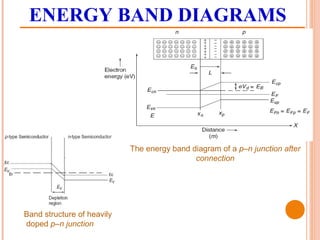


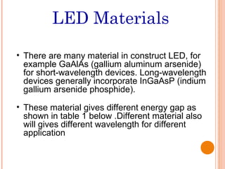


The document discusses optical fiber communication and p-n junctions. It describes how p-n junctions are formed through doping semiconductor materials with donor or acceptor impurities. This creates a concentration gradient that results in carrier diffusion and the formation of a p-n junction. The document then discusses energy band diagrams of p-n junctions and how applying voltage can change the potential barrier. It also summarizes the rectifying voltage-current characteristics and forward and reverse bias modes of p-n junction diodes. Finally, it briefly discusses light emitting diodes and their materials, structures, radiation patterns, and emission efficiency.