
Recommended
More Related Content
Similar to OFC PPT Optical Sources Unit 5-4-23.pptx
Similar to OFC PPT Optical Sources Unit 5-4-23.pptx (20)
Recently uploaded
Recently uploaded (20)
OFC PPT Optical Sources Unit 5-4-23.pptx
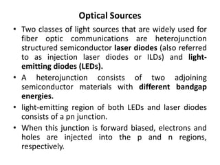
- 1. Optical Sources • Two classes of light sources that are widely used for fiber optic communications are heterojunction structured semiconductor laser diodes (also referred to as injection laser diodes or ILDs) and light- emitting diodes (LEDs). • A heterojunction consists of two adjoining semiconductor materials with different bandgap energies. • light-emitting region of both LEDs and laser diodes consists of a pn junction. • When this junction is forward biased, electrons and holes are injected into the p and n regions, respectively.
- 2. • These injected minority carriers can recombine either radiatively, in which case a photon of energy hv is emitted, or nonradiatively, whereupon the recombination energy is dissipated in the form of heat. • This pn junction is thus known as the active or recombination region. • A major difference between LEDs and laser diodes is that the optical output from an LED is incoherent (different frequency and phase difference), whereas that from a laser diode is coherent (same frequency and zero or constant phase difference).
- 3. • In a coherent source, the optical energy is produced in an optical resonant cavity. The optical energy released from this cavity has spatial and temporal coherence, which means it is highly monochromatic and the output beam is very directional. • In an incoherent LED source, no optical cavity exists for wavelength selectivity • spatial coherence = is correlation between waves at different points in space (tells directionality of laser beams) • temporal coherence= is a measure of average correlation between the value of a wave and itself delayed by time t. (tells how monochromatic a light is)
- 4. Characteristics of Light Source of Communication 1) It must be possible to operate the device continuously at a variety of temperatures for many years. 2) It must be possible to modulate the light output over a wide range of modulating frequencies. 3) For fiber links, the wavelength of the output should coincide with one of transmission windows for the fiber type used. 4) To couple large amount of power into an optical fiber, the emitting area should be small. 5) To reduce material dispersion in an optical fiber link, the output spectrum should be narrow. 6) The power requirement for its operation must be low. 7) The light source must be compatible with the modern solid state devices. 8) The optical output power must be directly modulated by varying the input current to the device. 9) Better linearity to prevent harmonics and intermodulation distortion. 10) High coupling efficiency. 11) High optical output power. 12) High reliability. 13) Low weight and low cost.
- 5. Light-Emitting Diodes (LEDs) • Conventional p-n junction is called as homojunction as, same semiconductor material is used on both sides of the junction. • The electron-hole recombination occurs in relatively wide layer = 10μm. As the carriers are not confined to the immediate vicinity of junction, hence high current densities can not be realized. • The carrier confinement problem can be resolved by sandwiching a thin layer ( = 0.1 μm) between p-type and n-type layers. • The carrier confinement occurs due to bandgap discontinuity of the junction. Such a junction is call heterojunction and the device is called double heterostructure.
- 6. • LEDs are best suitable optical source for an optical communication system when the requirements is – i) Bit rate f 100-200Mb/sec. ii) Optical power in tens of micro watts. LED Structures • To be useful in fiber transmission applications, an LED must have i. high radiance output, ii. fast emission response time, iii. high quantum efficiency.
- 7. • Its radiance (or brightness) is a measure, in watts, of the optical power radiated into a unit solid angle per unit area of the emitting surface. High radiances are necessary to couple sufficiently high optical power levels into a fiber. • The emission response time is the time delay between the application of a current pulse and the onset of optical emission. • The quantum efficiency is related to the fraction of injected electron–hole pairs that recombine radiatively.
- 8. • LED structure must provide a means of confining the charge carriers and the stimulated optical emission to the active region of the pn junction where radiative recombination takes place. • Carrier confinement is used to achieve a high level of radiative recombination in the active region of the device. • Optical confinement is of importance for preventing absorption of the emitted radiation by the material surrounding the pn junction.
- 9. • The most effective of these structures is the configuration shown in Fig. This is referred to as a double-heterostructure (or heterojunction) device because of the two different alloy layers on each side of the active region. • By means of this sandwich structure of differently composed alloy layers, both the carriers and the optical field are confined in the central active layer. • The bandgap differences of adjacent layers confine the charge carriers (as in b) while the differences in the indices of refraction of adjoining layers confine the optical field to the central active layer. (as in c)
- 11. • There are two main types of LED used in optical fiber links – 1. Surface emitting LED. 2. Edge emitting LED.
- 13. • In the surface emitter, the plane of the active light- emitting region is oriented perpendicularly to the axis of the fiber, as shown in Fig. • In this configuration, a well is etched through the substrate of the device, into which a fiber is then cemented in order to accept the emitted light. • The circular active area in practical surface emitters is nominally 50 mm in diameter and up to 2.5 mm thick. • The emission pattern is essentially isotropic with a 120° half-power beam width.
- 14. • This isotropic pattern from such a surface emitter is called a lambertian pattern. • In this pattern, the source is equally bright when viewed from any direction, but the power diminishes as cos θ, where θ is the angle between the viewing direction and the normal to the surface (this is because the projected area one sees decreases as cos θ). • Thus, the power is down to 50 percent of its peak when θ = 60°, so that the total half-power beam width is 120°.
- 16. • The edge emitter depicted in Fig.consists of an active junction region, which is the source of the incoherent light, and two guiding layers. • The guiding layers both have a refractive index lower than that of the active region but higher than the index of the surrounding material. • This structure forms a waveguide channel that directs the optical radiation toward the fiber core. • To match the typical fiber-core diameters (50–100 mm), the contact stripes for the edge emitter are 50–70 mm wide. Lengths of the active regions usually range from 100 to 150 mm. • The emission pattern of the edge emitter is more directional than that of the surface emitter, as is illustrated in Fig. • In the plane parallel to the junction, where there is no waveguide effect, the emitted beam is lambertian (varying as cos θ) with a half-power width of θ parallel = 120°. In the plane perpendicular to the junction, the half-power beam θ perpendicular has been made as small as 25–35° by a proper choice of the waveguide thickness.
- 17. Features of ELED • Linear relationship between optical output and current. • Spectral width is 25 to 400 nm for λ = 0.8 – 0.9 μm. • Modulation bandwidth is much large. • Are more reliable. • ELEDs have better coupling efficiency than surface emitter. • ELEDs are temperature sensitive. Usage : 1. LEDs are suited for short range narrow and medium bandwidth links. 2. Suitable for digital systems up to 140 Mb/sec. 3. Long distance analog links.
- 18. Light Source Materials • For operation in the 800-to-900-nm spectrum, the principal material used is the ternary alloy • The ratio x of aluminum arsenide to gallium arsenide determines the bandgap of the alloy and, correspondingly, the wavelength of the peak emitted radiation. • An example of the emission spectrum of a LED with x = 0.08 is shown in fig.
- 19. • The peak output power occurs at 810 nm. • The width of the spectral pattern at its half-power point is known as the full-width half maximum (FWHM) spectral width. • As shown in Fig. 4.12, this FWHM spectral width is 36 nm.
- 20. • At longer wavelengths the which is a quaternary alloy is one of the primary material candidates. • Using the fundamental quantum mechanical relationship between energy E and frequency v, • The peak emission wavelength λ in micrometers can be expressed as a function of the bandgap energy Eg in electron volts by the equation
- 21. • The bandgap energy (Eg) can be controlled by two compositional parameters x and y, within direct bandgap region. • In the ternary alloy GaAlAs the bandgap energy Eg in electron volts for values of x between zero and 0.37 can be found from the empirical equation • In the quaternary alloy expression relating Eg and x,y are
- 22. Problem: Compute the emitted wavelength from a ternary optical source having x = 0.07. Soln:
- 23. Problem: Consider the material alloy Find (a) the bandgap of this material; (b) the peak emission wavelength • Soln: Comparing the alloy with the quaternary alloy composition it is found that x = 0.26 and y = 0.57
- 24. Quantum Efficiency and LED Power • The internal quantum efficiency in the active region is the fraction of the electron–hole pairs that recombine radiatively. • If the radiative recombination rate is Rr and the nonradiative recombination rate is Rnr, then the internal quantum efficiency ηint is the ratio of the radiative recombination rate to the total recombination rate
- 25. • The radiative recombination lifetime is τr = n/Rr • The nonradiative recombination lifetime is τnr = n/Rnr. • Thus the internal quantum efficiency can be expressed as
- 26. • If the current injected into the LED is I and q is electron charge then total number of recombinations per second is Rr + Rnr = I/q Substituting this in quantum efficiency equation
- 28. Advantages of LED 1. Simple design. 2. Ease of manufacture. 3. Simple system integration. 4. Low cost. 5. High reliability. Disadvantages of LED 1. Refraction of light at semiconductor/air interface. 2. The average life time of a radiative recombination is only a few nanoseconds, therefore modulation BW is limited to only few hundred megahertz. 3. Low coupling efficiency. 4. Large chromatic dispersion.
- 29. Injection Laser Diode (ILD) • The laser is a device which amplifies the light, hence the LASER is an acronym for Light Amplification by Stimulated Emission of Radiation. • The operation of the device may be described by the formation of an electromagnetic standing wave within a cavity which provides an output of monochromatic highly coherent radiation. • Material absorb light than emitting. Three different fundamental process occurs between the two energy states of an atom. 1) Absorption 2) Spontaneous emission 3) Stimulated emission.
- 30. • Laser action is the result of three process absorption of energy packets (photons), spontaneous emission, and stimulated emission. (These processes are represented by the simple two-energy-level diagrams). Where E1 is the lower state energy level. E2 is the higher state energy level.
- 31. • Quantum theory states that any atom exists only in certain discrete energy state, absorption or emission of light causes them to make a transition from one state to another. • The frequency of the absorbed or emitted radiation f is related to the difference in energy E between the two states. • If E1 is lower state energy level, E2 is higher state energy level. • E = (E2 – E1) = h.f • Where, h = 6.626 x 10⁻³⁴ J/s (Plank’s constant).
- 32. • An atom is initially in the lower energy state, when the photon with energy (E2 – E1) is incident on the atom, it will be excited into the higher energy state E2 through the absorption of the photon.
- 33. • When the atom is initially in the higher energy state E2, it can make a transition to the lower energy state E1 providing the emission of a photon at a frequency corresponding to E = h.f. The emission process can occur in two ways. A) By spontaneous emission in which the atom returns to the lower energy state in random manner. B) By stimulated emission when a photon having equal energy to the difference between the two states (E2 – E1) interacts with the atom causing it to the lower state with the creation of the second photon.
- 35. • Spontaneous emission gives incoherent radiation while stimulated emission gives coherent radiation. • Hence the light associated with emitted photon is of same frequency of incident photon, and in same phase. • It means that when an atom is stimulated to emit light energy by an incident wave, the liberated energy can add to the wave in constructive manner. • The emitted light is bounced back and forth internally between two reflecting surface. • The bouncing back and forth of light wave cause their intensity to reinforce and build-up. The result in a high brilliance, single frequency light beam providing amplification.