Module_5_1.pptxsatellite and optical communication
1.
MODULE–5 Syllabus
MODULE –5.1
Optical sources: Light Emitting diodes: LED Structures, Light Source
Materials, Quantum Efficiency and LED Power, Modulation. Laser Diodes:
Modes and Threshold conditions, Rate equation, External Quantum
Efficiency, Resonant frequencies, Laser Diode structures and Radiation
Patterns: Single mode lasers.
Photo Detectors: Physical principles of Photodiodes, Photo detector noise,
Detector response time.
2.
Optical Sources
ABasic Optical Communication System consists of Essentially three
Components they are Optical Source, An Optical Fiber, and a Photo
Detector.
The Role of an Optical Source is to convert Electrical Signal into an
Optical Signal.
•The Major Requirements of the Optical Source are
Ability to Directly Modulate the Light Intensity
Compatibility to Optical Fibers – In terms of the Operating
Wavelength, and Power Coupling
Spectral Width and Reasonable Optical Power Outputs.
Most Suitable Optical Sources are
Semiconductor Light Emitting Diodes (LED)
Laser Diodes (LD)
3.
Optical Sources
LightEmitting Diode (LED): A Light Emitting Diode is a
Semiconductor device that emits narrow beam of light under
Forward bias Condition.
Light from LED is Non-Coherent.
LED consists of semiconductor material, doped with impurities to create
a structure called p-n junction and current flows in one direction.
When Electrons and holes flow into the junction from electrodes
with different voltages, electron falls into lower energy level and
release energy in the form of photon in the Visible Spectrum.
The Wavelength of the Light (Color) depends on the band gap energy
of the material forming the p-n junction.
LED’s are built on n-type substrate with electrodes attached to p-type
layer deposited on its surface.
4.
Optical Sources
TheRefractive Index (RI) of the package material must match with
the RI of the Semiconductor otherwise Light gets partially reflected
back, which is absorbed and turns into Heat.
The Major Breakthrough that Led to High Capacity with the invention
of LASER (Light Amplification by Stimulated Emission of Radiation )
in 1960.
LASER action results from following phenomena
Photon Absorption
Spontaneous Emission
Stimulated Emission (By Population Inversion)
5.
LED STRUCTURES
Light EmittingDiodes(LEDs) :
p-n Junction
Conventional p-n junction is called as homojunction as same
semiconductor material is used on both sides junction. The electron-hole
recombination occurs in relatively wide layer = 10 μm. As the carriers
are not confined to the immediate vicinity of junction, hence high
current densities can not be realized.
The carrier confinement problem can be resolved by sandwiching a thin
layer ( = 0.1 μm) between p-type and n-type layers. The middle
layer may or may not be doped. The carrier confinement occurs due to
bandgap discontinuity of the junction. Such a junction is called hetero
junction and the device is called double hetero structure.
6.
LED STRUCTURES
Forany Optical Communication systems requiring Bit rate less than
100-200Mb/sec together with Multimode Fiber coupled optical power
in tens of micro watts. LEDs (Semiconductor Light Emitting Diode)
are best suitable optical source.
These LEDs require i) less complex drive circuitry than the Laser
diode.
ii) No Thermal or optical stabilization circuits needed
iii) fabricated with low cost
To achieve a high Radiance and a high quantum efficiency, the LED
structure a means of confining the charge carriers and the stimulated
optical emission to the active region of the pn junction where
Radioactive recombination takes place
7.
LED STRUCTURES
ForCarrier Confinement is used to achieve a high level of Radiative
recombination in the active region of the device, which yields a high
quantum efficiency.
Optical Confinement is of importance for preventing absorption of the
emitted radiation by the material surrounding the pn junction.
To achieve carrier and optical confinements LED Structure
configuration are of two types such as
i)HOMO JUNCTION
ii) SINGLE and DOUBLE HETROJUNCTION are widely used
8.
LED STRUCTURES
Heterojuncitons
Ajunction is an interface between two adjoining single crystal
semiconductors with different band gap.
Heterojunctions are of two types,
Isotype (n-n or p-p) or Antisotype (p-n).
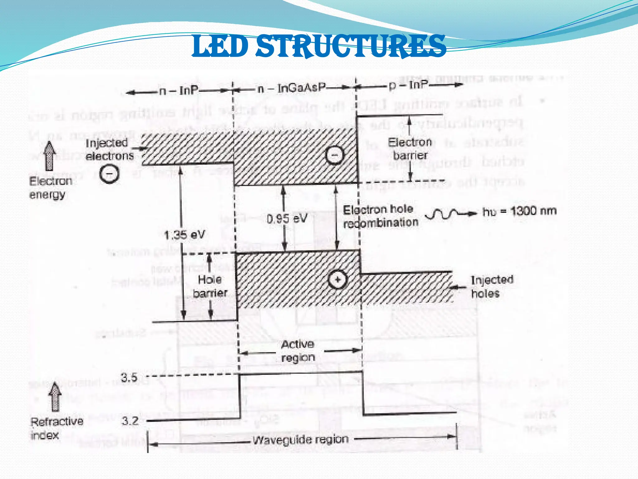
Double Heterojunctions (DH)
In order to achieve efficient confinement of emitted radiation double
hetero junction are used in LED structure. A hetero junction is a
junction formed by dissimilar semiconductors. Double hetero junction
(DH) is formed by two different semiconductors on each side of active
region. Fig. shows double hetero junction (DH) light emitter.
9.
LED STRUCTURES
Heterojuncitons
Ajunction is an interface between two adjoining single crystal
semiconductors with different band gap.
Heterojunctions are of two types,
Isotype (n-n or p-p) or Antisotype (p-n).
Double Heterojunctions (DH)
In order to achieve efficient confinement of emitted radiation double
hetero junction are used in LED structure. A hetero junction is a
junction formed by dissimilar semiconductors. Double hetero junction
(DH) is formed by two different semiconductors on each side of active
region. Fig. shows double hetero junction (DH) light emitter.
Led structures
•The crosshatchedregions represent the energy levels of freecharge.
Recombination occurs only in active InGaAsP layer.
•The two materials have different band gap energies and different
refractive indices. The changes in band gap energies create potential
barrier for both holes and electrons. The free charges can recombine only in
narrow, well defined active layer side.
•A Double Heterojunction (DH) structure will confine both hole and electrons
to a narrow active layer. Under forward bias, there will be a large number of
carriers injected into active region where they are efficiently confined.
Carrier recombination occurs in small active region so leading to an efficient
device.
•Another advantage DH structure is that the active region has a higher
refractive index than the materials on either side, hence light emission
occurs in an optical waveguide, which serves to narrow the output beam.
12.
Led structures cont..
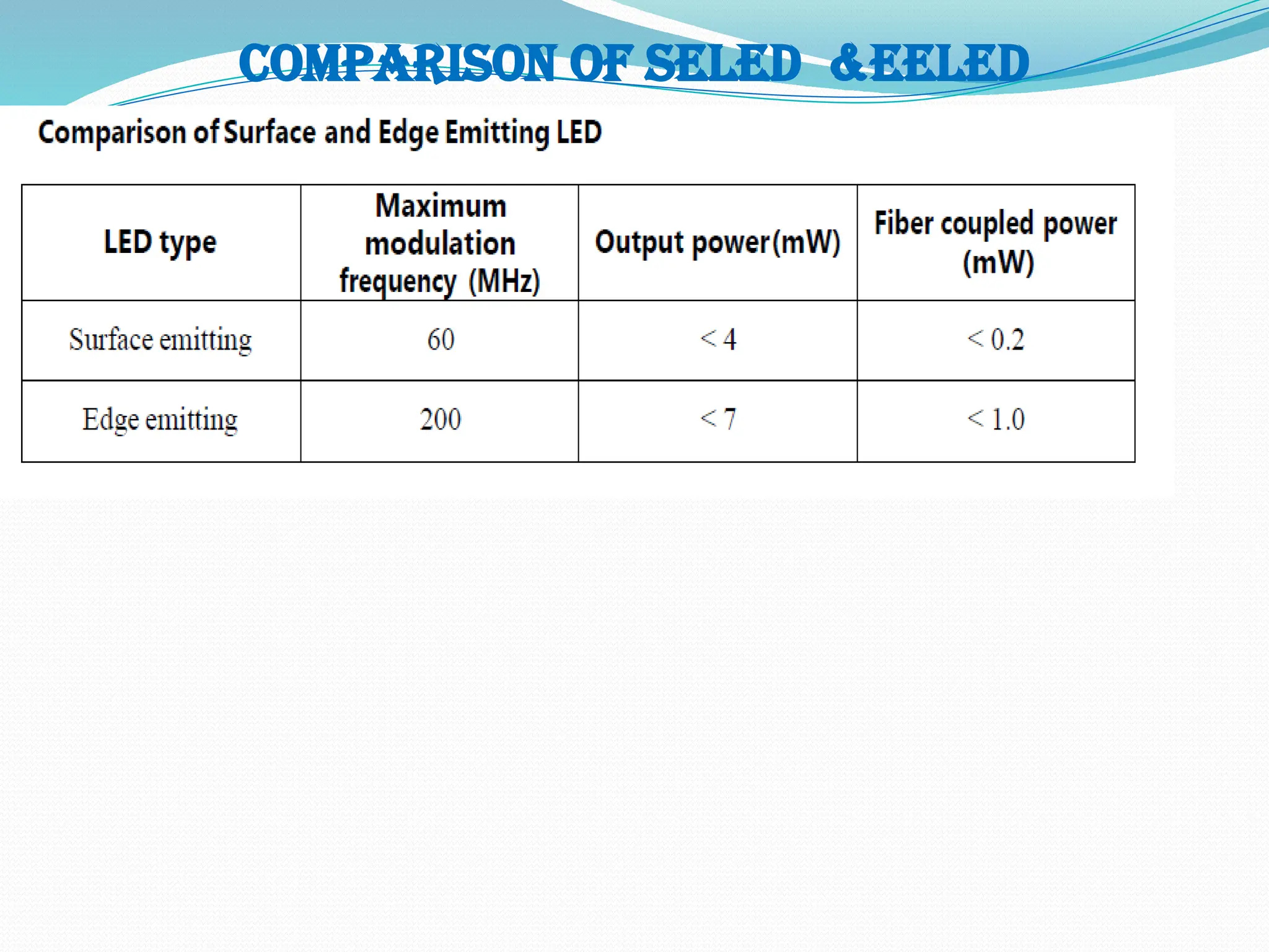
LEDconfigurations :At present there are two main types of LED used in optical
fiber links – 1. Surface emitting LED. 2. Edge emitting LED.
•Both devices used a DH structure to constrain the carriers and the light to an
active layer.
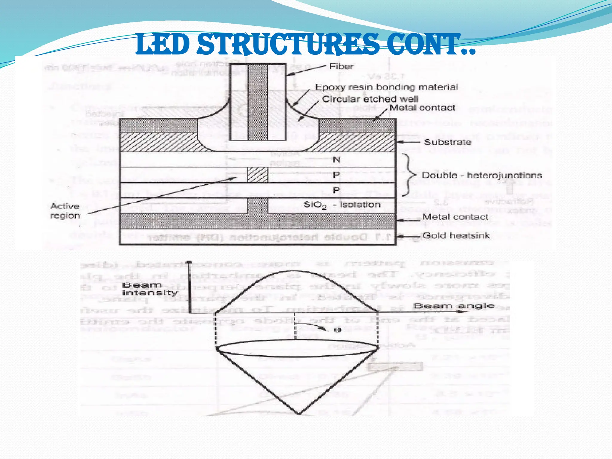
Surface Emitting LEDs
•In surface emitting LEDs the plane of active light emitting region is oriented
perpendicularly to the axis of the fiber. A DH diode is grown on an N-type
substrate at the top of the diode as shown in Fig. A circular well is etched
through the substrate of the device. A fiber is then connected to accept the
emitted light.
•At the back of device is a gold heat sink. The current flows through the
p-type material and forms the small circular active region resulting in the
intense beam of light.
Led structures cont..
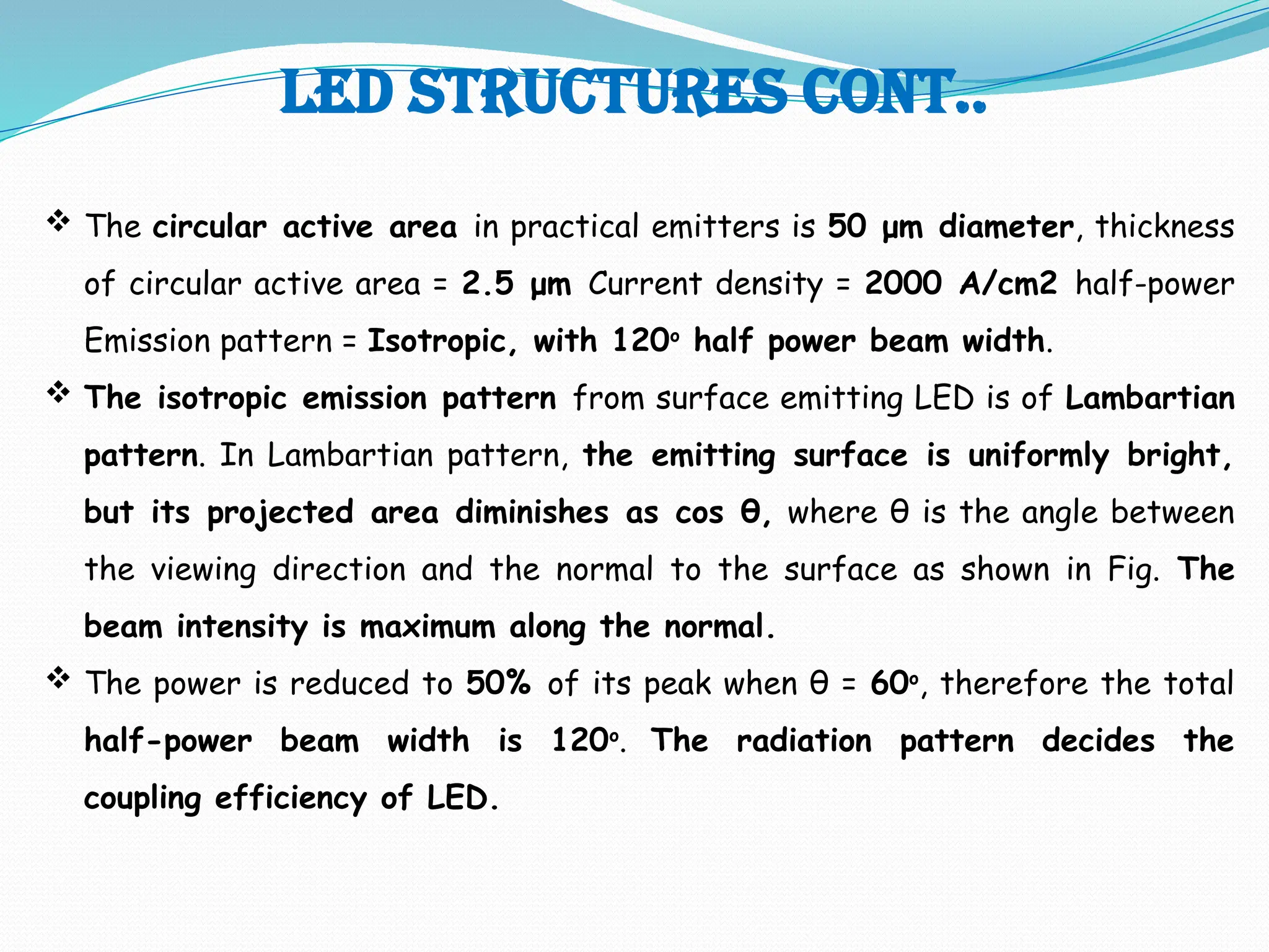
The circular active area in practical emitters is 50 μm diameter, thickness
of circular active area = 2.5 μm Current density = 2000 A/cm2 half-power
Emission pattern = Isotropic, with 120o
half power beam width.
The isotropic emission pattern from surface emitting LED is of Lambartian
pattern. In Lambartian pattern, the emitting surface is uniformly bright,
but its projected area diminishes as cos θ, where θ is the angle between
the viewing direction and the normal to the surface as shown in Fig. The
beam intensity is maximum along the normal.
The power is reduced to 50% of its peak when θ = 60o
, therefore the total
half-power beam width is 120o
. The radiation pattern decides the
coupling efficiency of LED.
15.
Led structures cont..
•EdgeEmitting LEDS (ELEDs) :
•In order to reduce the losses caused by absorption in the active layer and
to make the beam more directional, the light is collected from the edge of
the LED. Such a device is known as Edge Emitting LED or ELED.
•It consists of an active junction region which is the source of incoherent light
and two guiding layers. The refractive index of guiding layers is lower than
active region but higher than outer surrounding material. Thus a waveguide
channel is form and optical radiation is directed into the fiber. Fig shows
structure of ELED.
•Edge emitter‘s emission pattern is more concentrated (directional) providing
improved coupling efficiency. The beam is Lambartian in the plane parallel to
the junction but diverges more slowly in the plane perpendicular to the
junction.
16.
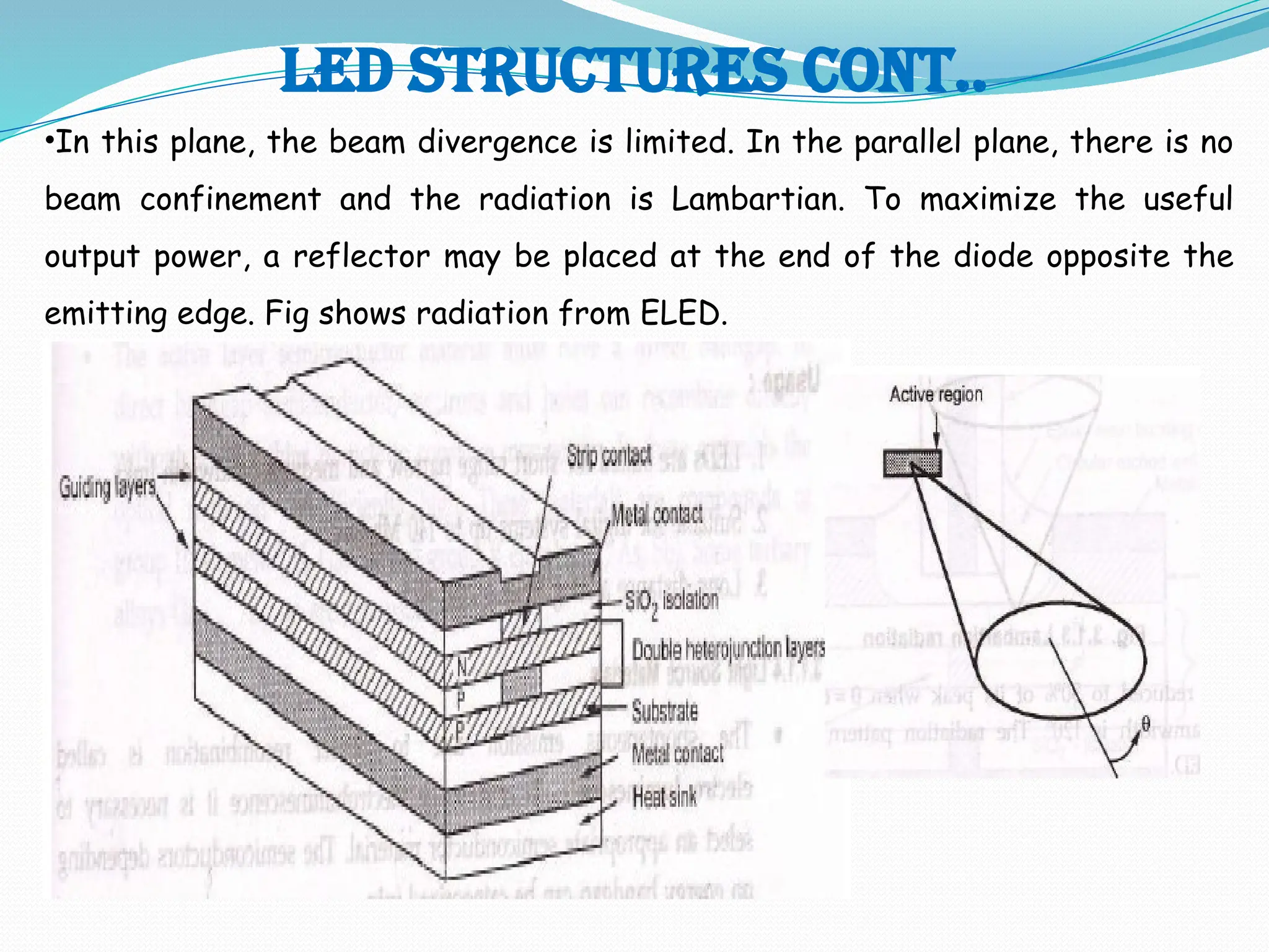
Led structures cont..
•Inthis plane, the beam divergence is limited. In the parallel plane, there is no
beam confinement and the radiation is Lambartian. To maximize the useful
output power, a reflector may be placed at the end of the diode opposite the
emitting edge. Fig shows radiation from ELED.
17.
Led structures cont..
•Featuresof ELED:
1. Linear relationship between optical output and current.
2. Spectral width is 25 to 400 nm for λ = 0.8 – 0.9 μm.
3. Modulation bandwidth is much large.
4. Not affected by catastrophic gradation mechanisms hence are more reliable.
5. ELEDs have better coupling efficiency than surface emitter.
6. ELEDs are temperature sensitive.
•Usage :
1. LEDs are suited for short range narrow and medium bandwidth links.
2. Suitable for digital systems up to 140 Mb/sec.
3. Long distance analog links.
18.
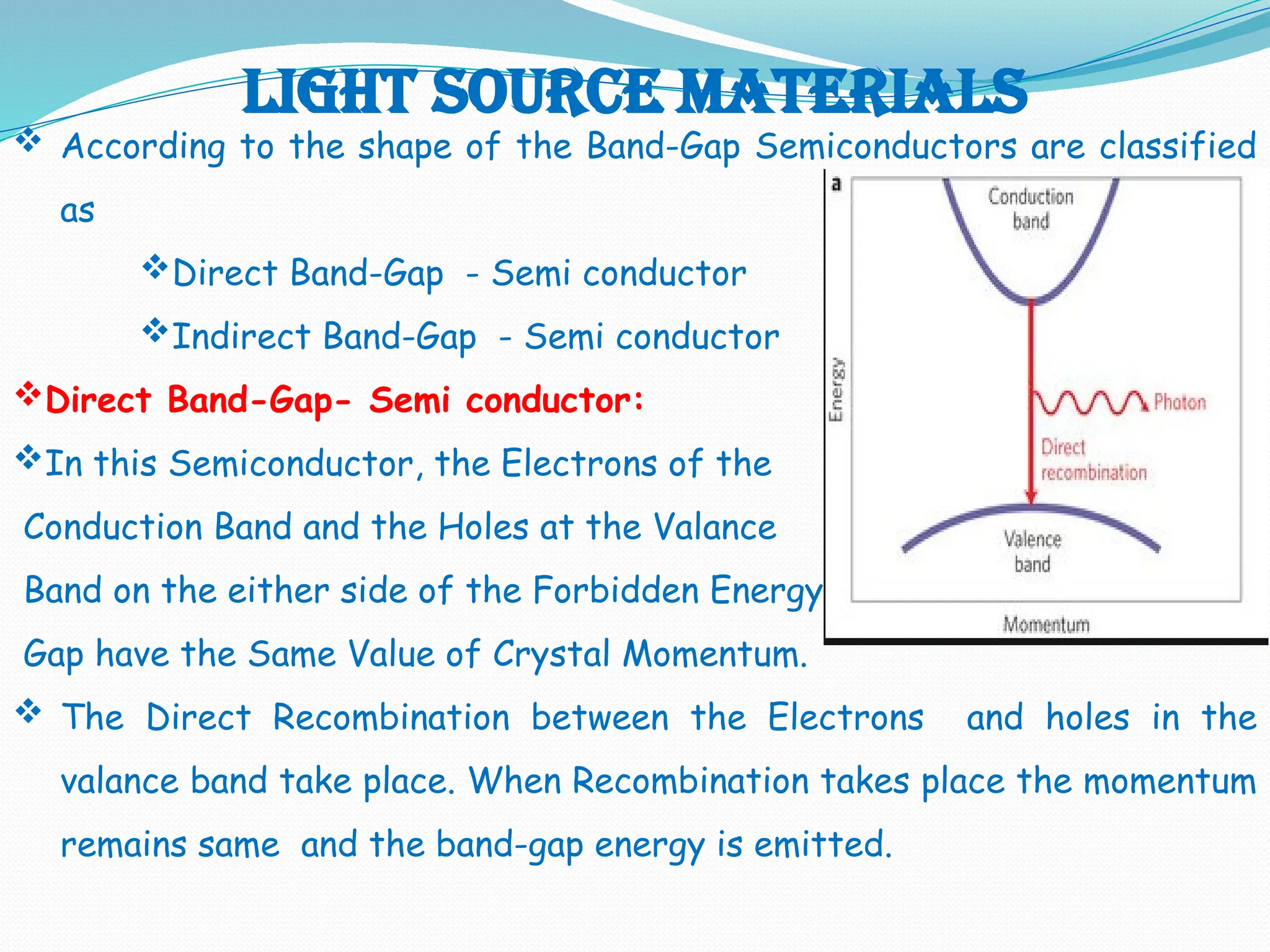
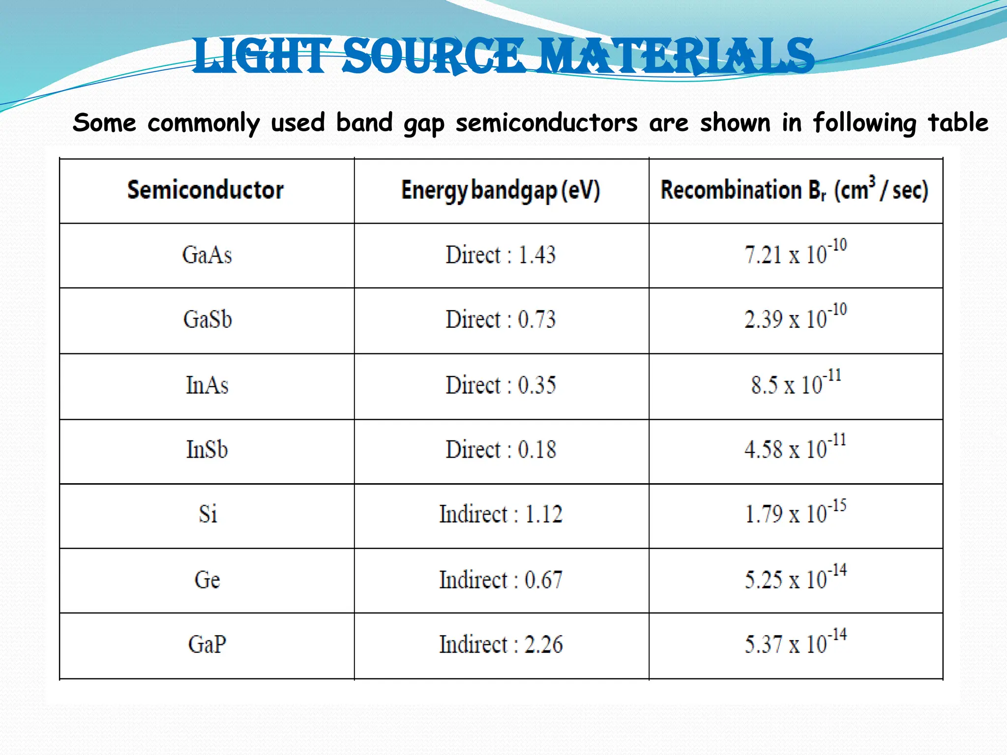
Light source materials
According to the shape of the Band-Gap Semiconductors are classified
as
Direct Band-Gap - Semi conductor
Indirect Band-Gap - Semi conductor
Direct Band-Gap- Semi conductor:
In this Semiconductor, the Electrons of the
Conduction Band and the Holes at the Valance
Band on the either side of the Forbidden Energy
Gap have the Same Value of Crystal Momentum.
The Direct Recombination between the Electrons and holes in the
valance band take place. When Recombination takes place the momentum
remains same and the band-gap energy is emitted.
19.
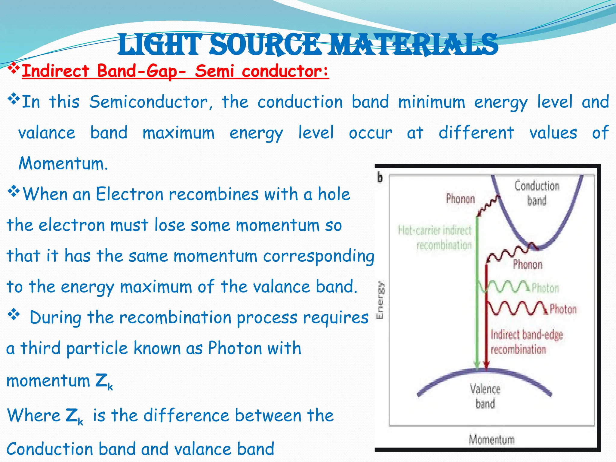
Light source materials
IndirectBand-Gap- Semi conductor:
In this Semiconductor, the conduction band minimum energy level and
valance band maximum energy level occur at different values of
Momentum.
When an Electron recombines with a hole
the electron must lose some momentum so
that it has the same momentum corresponding
to the energy maximum of the valance band.
During the recombination process requires
a third particle known as Photon with
momentum Zk
Where Zk is the difference between the
Conduction band and valance band
20.
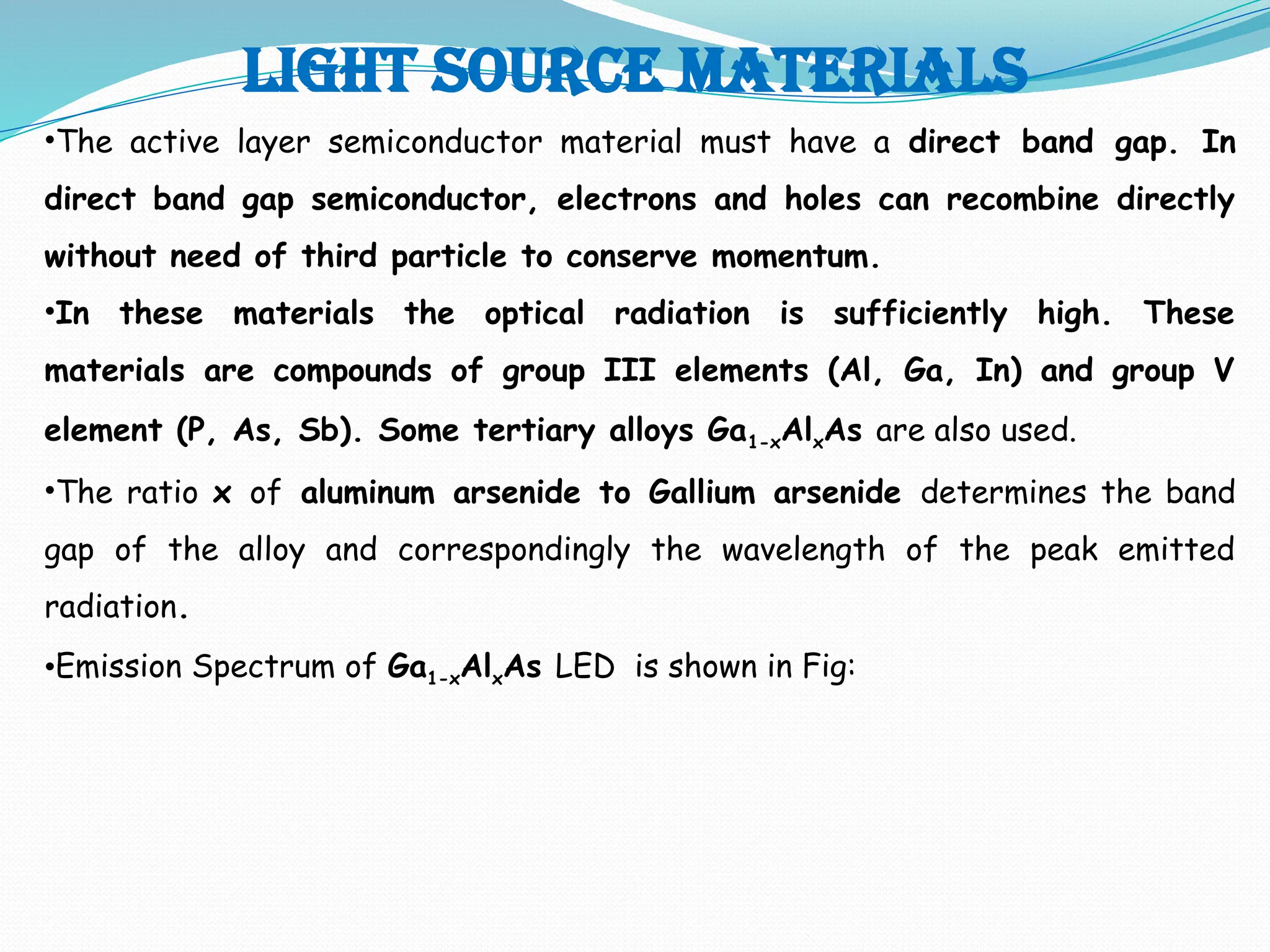
Light source materials
•Theactive layer semiconductor material must have a direct band gap. In
direct band gap semiconductor, electrons and holes can recombine directly
without need of third particle to conserve momentum.
•In these materials the optical radiation is sufficiently high. These
materials are compounds of group III elements (Al, Ga, In) and group V
element (P, As, Sb). Some tertiary alloys Ga1-xAlxAs are also used.
•The ratio x of aluminum arsenide to Gallium arsenide determines the band
gap of the alloy and correspondingly the wavelength of the peak emitted
radiation.
•Emission Spectrum of Ga1-xAlxAs LED is shown in Fig:
21.
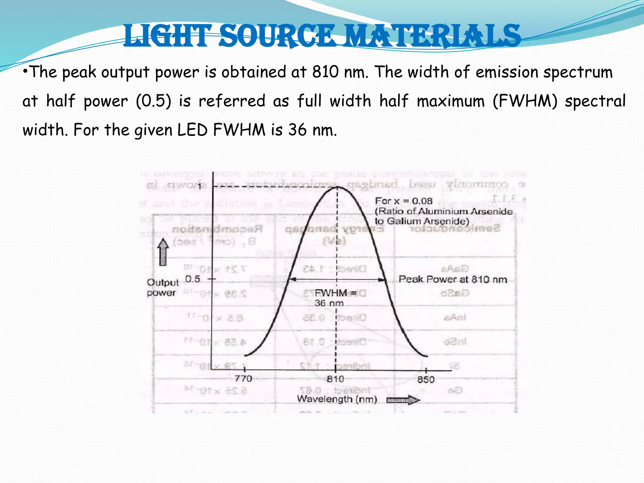
Light source materials
•Thepeak output power is obtained at 810 nm. The width of emission spectrum
at half power (0.5) is referred as full width half maximum (FWHM) spectral
width. For the given LED FWHM is 36 nm.
22.
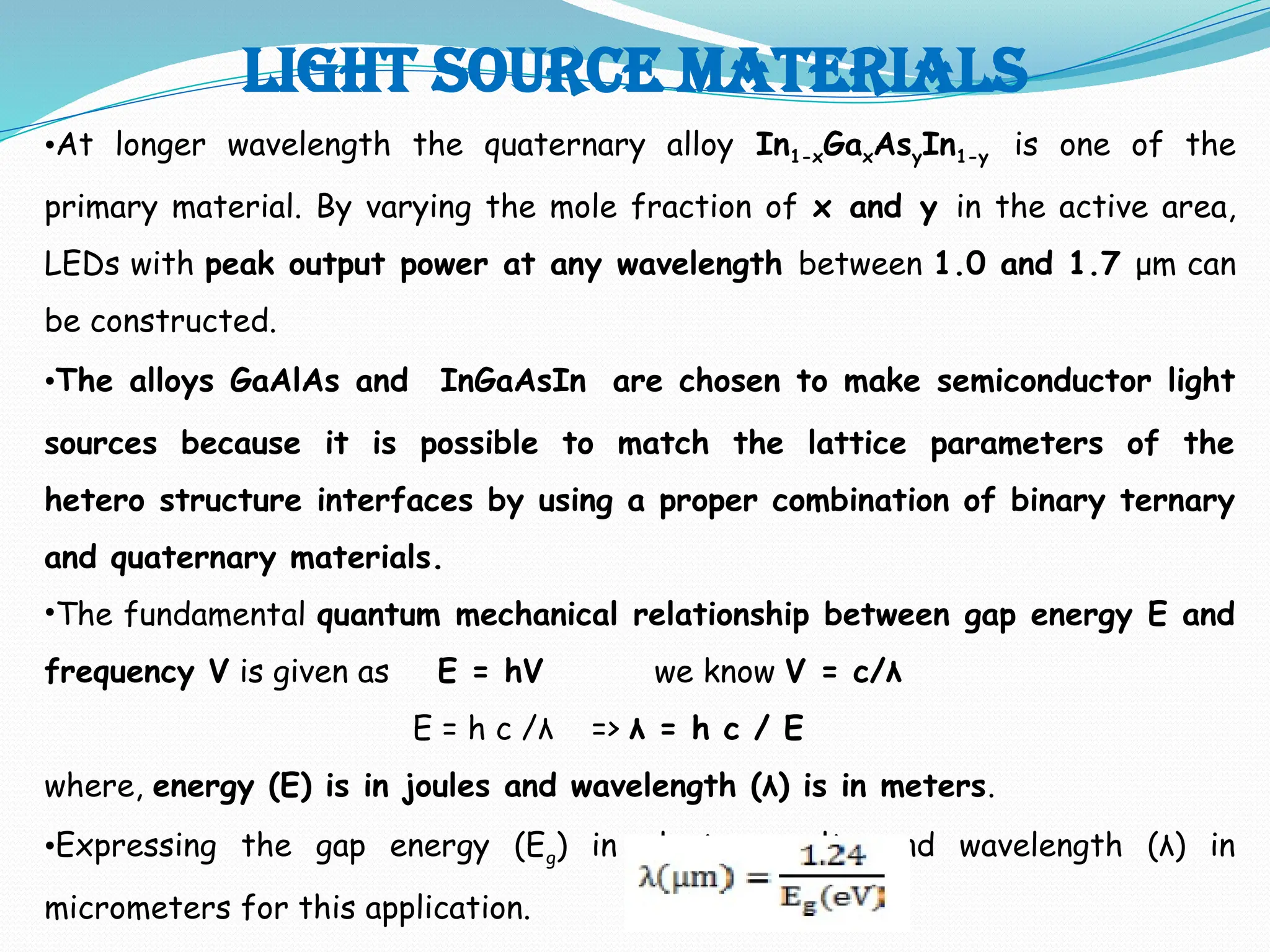
Light source materials
•Atlonger wavelength the quaternary alloy In1-xGaxAsyIn1-y is one of the
primary material. By varying the mole fraction of x and y in the active area,
LEDs with peak output power at any wavelength between 1.0 and 1.7 μm can
be constructed.
•The alloys GaAlAs and InGaAsIn are chosen to make semiconductor light
sources because it is possible to match the lattice parameters of the
hetero structure interfaces by using a proper combination of binary ternary
and quaternary materials.
•The fundamental quantum mechanical relationship between gap energy E and
frequency V is given as E = hV we know V = c/λ
E = h c /λ => λ = h c / E
where, energy (E) is in joules and wavelength (λ) is in meters.
•Expressing the gap energy (Eg) in electron volts and wavelength (λ) in
micrometers for this application.
23.
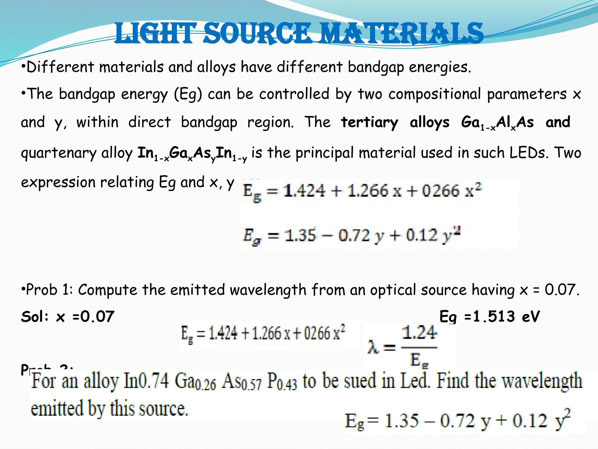
Light source materials
•Differentmaterials and alloys have different bandgap energies.
•The bandgap energy (Eg) can be controlled by two compositional parameters x
and y, within direct bandgap region. The tertiary alloys Ga1-xAlxAs and
quartenary alloy In1-xGaxAsyIn1-y is the principal material used in such LEDs. Two
expression relating Eg and x, y are –
•Prob 1: Compute the emitted wavelength from an optical source having x = 0.07.
Sol: x =0.07 Eg =1.513 eV
Prob 2:
Quantum efficiency &LED POWER
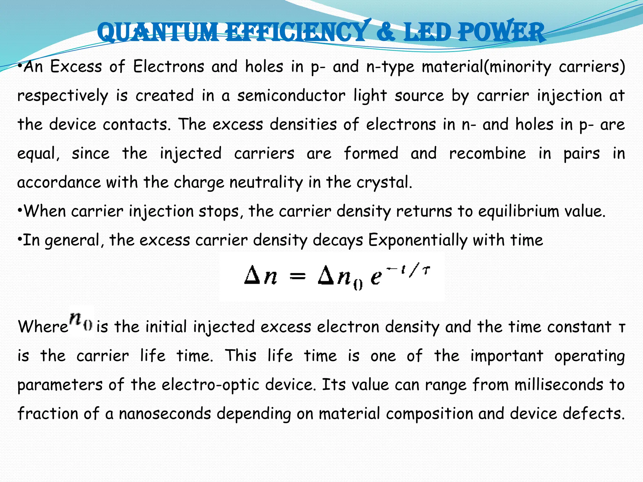
•An Excess of Electrons and holes in p- and n-type material(minority carriers)
respectively is created in a semiconductor light source by carrier injection at
the device contacts. The excess densities of electrons in n- and holes in p- are
equal, since the injected carriers are formed and recombine in pairs in
accordance with the charge neutrality in the crystal.
•When carrier injection stops, the carrier density returns to equilibrium value.
•In general, the excess carrier density decays Exponentially with time
Where is the initial injected excess electron density and the time constant τ
is the carrier life time. This life time is one of the important operating
parameters of the electro-optic device. Its value can range from milliseconds to
fraction of a nanoseconds depending on material composition and device defects.
26.
Quantum efficiency &LED POWER
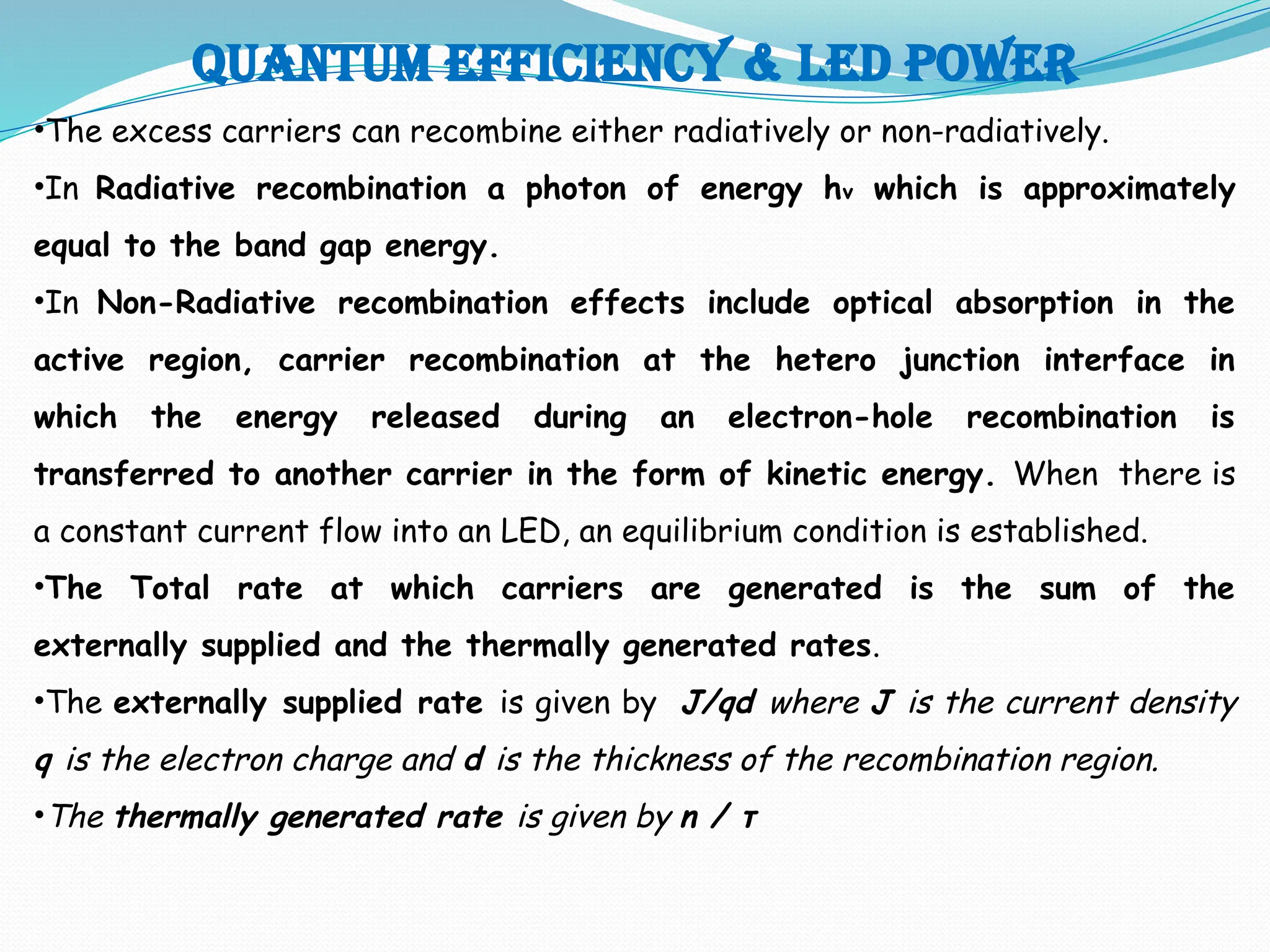
•The excess carriers can recombine either radiatively or non-radiatively.
•In Radiative recombination a photon of energy hv which is approximately
equal to the band gap energy.
•In Non-Radiative recombination effects include optical absorption in the
active region, carrier recombination at the hetero junction interface in
which the energy released during an electron-hole recombination is
transferred to another carrier in the form of kinetic energy. When there is
a constant current flow into an LED, an equilibrium condition is established.
•The Total rate at which carriers are generated is the sum of the
externally supplied and the thermally generated rates.
•The externally supplied rate is given by J/qd where J is the current density
q is the electron charge and d is the thickness of the recombination region.
•The thermally generated rate is given by n / τ
27.
Quantum efficiency &LED POWER
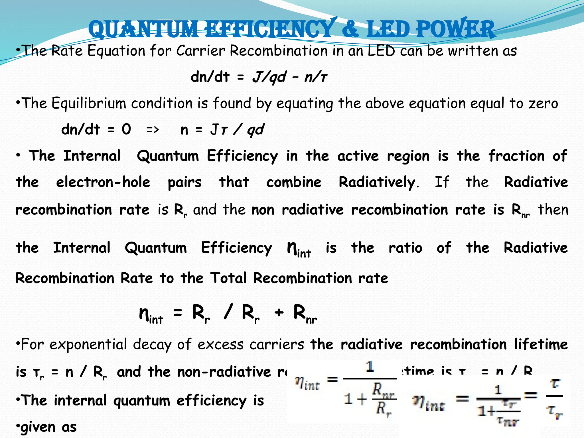
•The Rate Equation for Carrier Recombination in an LED can be written as
dn/dt = J/qd – n/τ
•The Equilibrium condition is found by equating the above equation equal to zero
dn/dt = 0 => n = Jτ / qd
• The Internal Quantum Efficiency in the active region is the fraction of
the electron-hole pairs that combine Radiatively. If the Radiative
recombination rate is Rr and the non radiative recombination rate is Rnr then
the Internal Quantum Efficiency ηint is the ratio of the Radiative
Recombination Rate to the Total Recombination rate
ηint = Rr / Rr + Rnr
•For exponential decay of excess carriers the radiative recombination lifetime
is τr = n / Rr and the non-radiative recombination lifetime is τnr = n / Rnr
•The internal quantum efficiency is
•given as
28.
Quantum efficiency &LED POWER
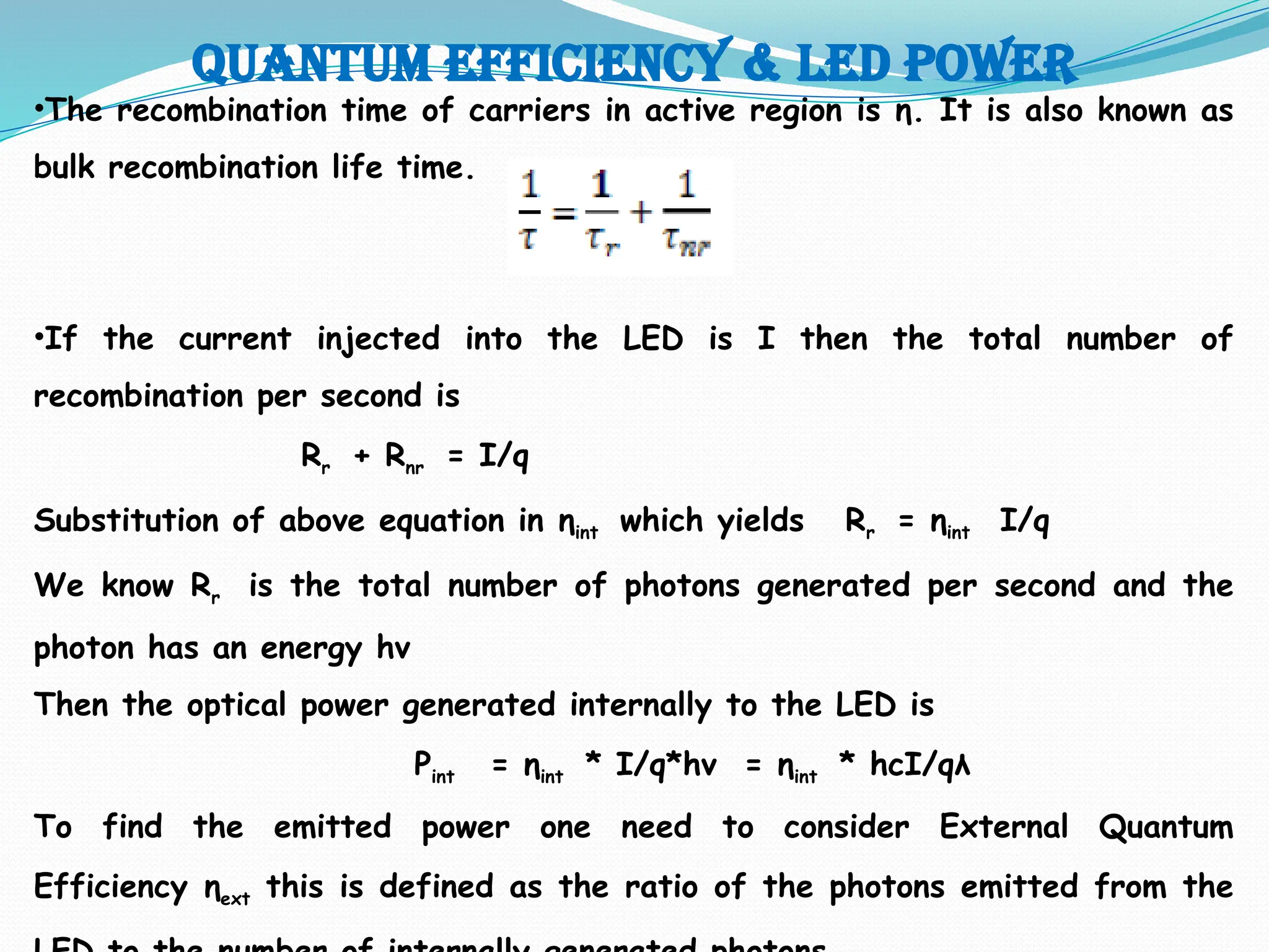
•The recombination time of carriers in active region is η. It is also known as
bulk recombination life time.
•If the current injected into the LED is I then the total number of
recombination per second is
Rr + Rnr = I/q
Substitution of above equation in ηint which yields Rr = ηint I/q
We know Rr is the total number of photons generated per second and the
photon has an energy hv
Then the optical power generated internally to the LED is
Pint = ηint * I/q*hv = ηint * hcI/qλ
To find the emitted power one need to consider External Quantum
Efficiency ηext this is defined as the ratio of the photons emitted from the
29.
Quantum efficiency &LED POWER
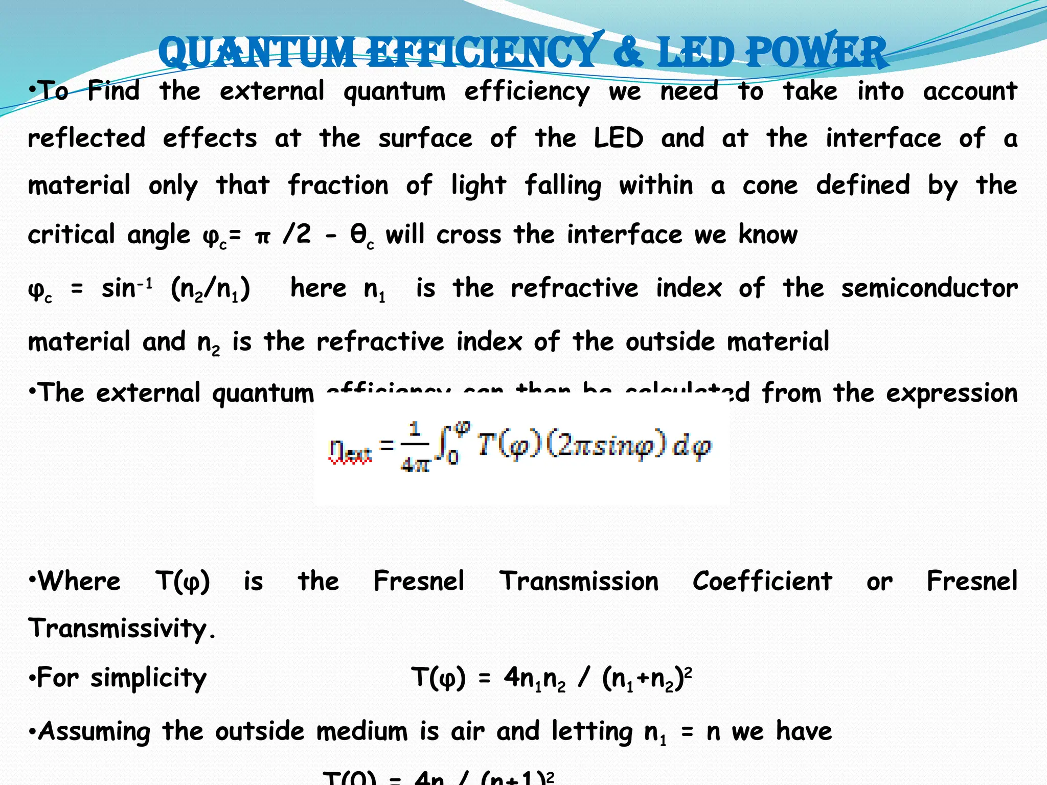
•To Find the external quantum efficiency we need to take into account
reflected effects at the surface of the LED and at the interface of a
material only that fraction of light falling within a cone defined by the
critical angle φc= π /2 - θc will cross the interface we know
φc = sin-1
(n2/n1) here n1 is the refractive index of the semiconductor
material and n2 is the refractive index of the outside material
•The external quantum efficiency can then be calculated from the expression
•Where T(φ) is the Fresnel Transmission Coefficient or Fresnel
Transmissivity.
•For simplicity T(φ) = 4n1n2 / (n1+n2)2
•Assuming the outside medium is air and letting n1 = n we have
2
30.
Quantum efficiency &LED POWER
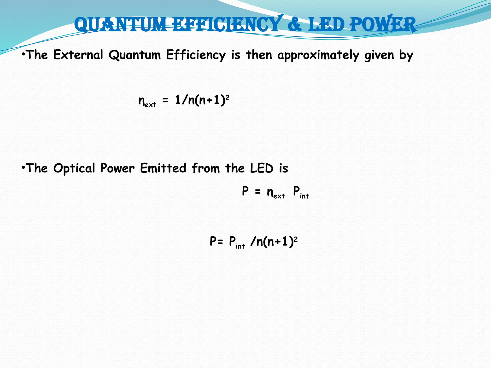
•The External Quantum Efficiency is then approximately given by
ηext = 1/n(n+1)2
•The Optical Power Emitted from the LED is
P = ηext Pint
P= Pint /n(n+1)2
31.
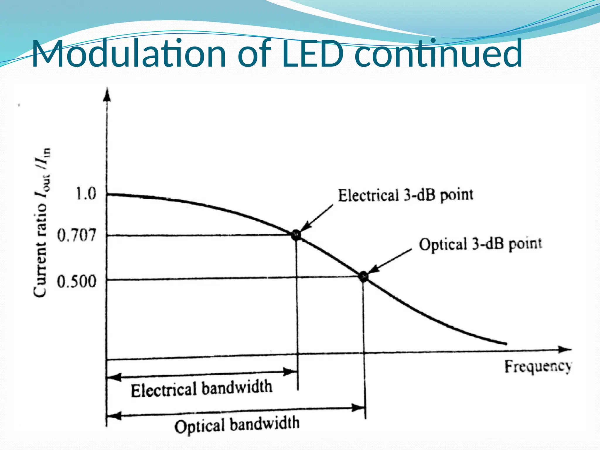
Modulation of anled
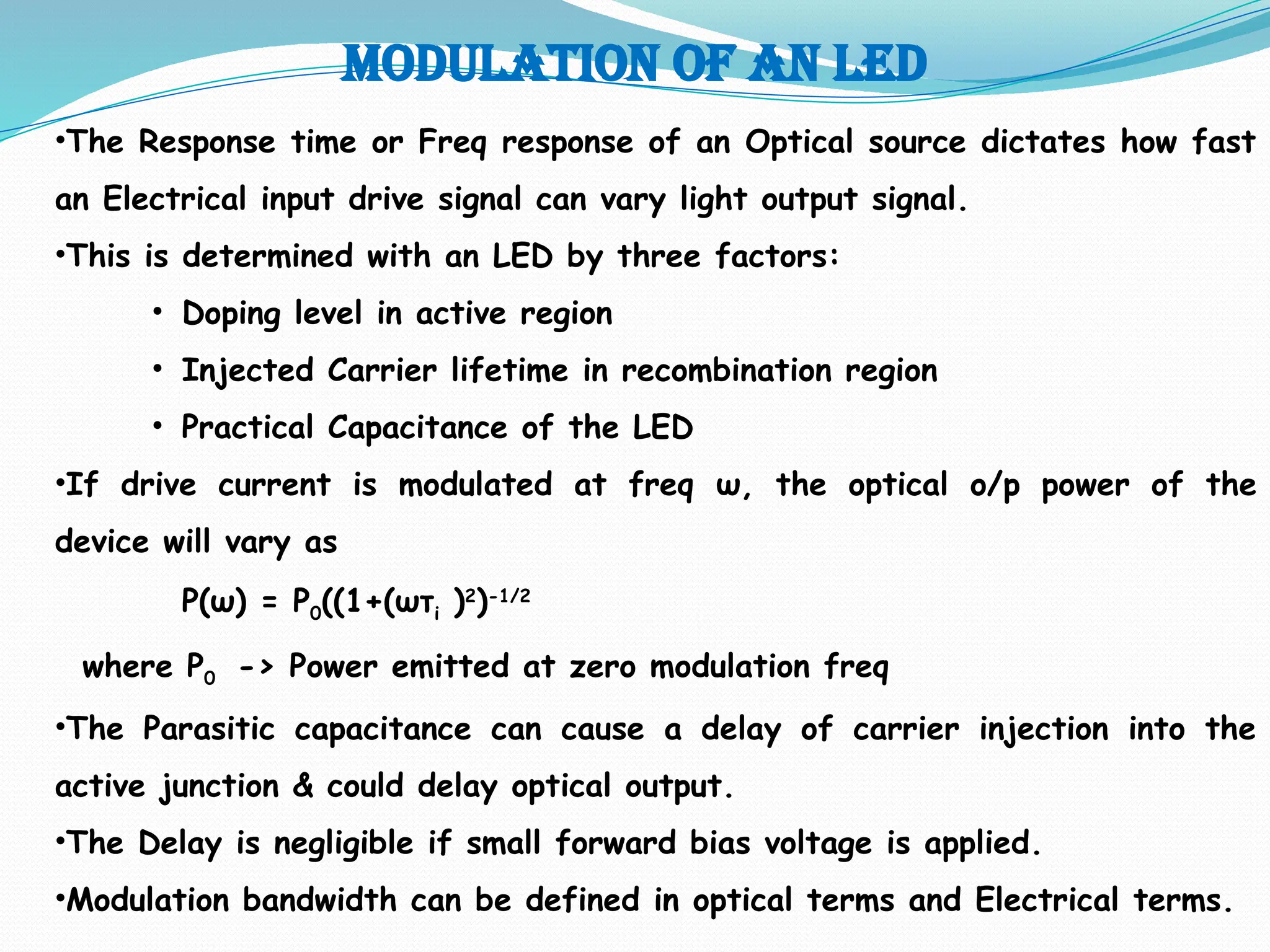
•The Response time or Freq response of an Optical source dictates how fast
an Electrical input drive signal can vary light output signal.
•This is determined with an LED by three factors:
• Doping level in active region
• Injected Carrier lifetime in recombination region
• Practical Capacitance of the LED
•If drive current is modulated at freq ω, the optical o/p power of the
device will vary as
P(ω) = P0((1+(ωτi )2
)-1/2
where P0 -> Power emitted at zero modulation freq
•The Parasitic capacitance can cause a delay of carrier injection into the
active junction & could delay optical output.
•The Delay is negligible if small forward bias voltage is applied.
•Modulation bandwidth can be defined in optical terms and Electrical terms.
Modulation of anled
•Electrical Modulation is defined as where Electrical Power has dropped to
half its constant value due to modulated portion of the Optical signal
•Electrical 3-dB Point: Freq at which output electrical power is reduced by
1/√2 w.r.t input electrical power.
•Optical Bandwidth: Freq at which output optical power is reduced by 1/2
•Electrical Bandwidth is defined by Freq when the output current has
dropped 1/√2 or 0.707 of input current to the system.
•Comparing Optical Bandwidth > Electrical Bandwidth.
BWoptical = √2 BWelectrical
34.
Advantages & disadvantagesof led
Advantages and Disadvantages of LED Advantages of LED
1. Simple design.
2. Ease of manufacture.
3. Simple system integration.
4. Low cost.
5. High reliability.
Disadvantages of LED
1. Refraction of light at semiconductor/air interface.
2. The average life time of a radiative recombination is only a few
nanoseconds, therefore Modulation BW is limited to only few hundred
megahertz.
3. Low coupling efficiency.
4. Large chromatic dispersion.
problems
Prob 1 :The radiative and non radiative recombination life times of
minority carriers in the active region of a double heterojunction LED
are 60 nsec and 90 nsec respectively. Determine the total carrier
recombination life time and optical power generated internally if the
peak emission wavelength si 870 nm and the drive currect is 40 mA.
[July/Aug.-2006, 6 Marks]
Prob 2:A double heterjunciton InGaAsP LED operating at 1310 nm has
radiative and non-radiative recombination times of 30 and 100 ns
respectively. The current injected is 40 Ma. Calculate –
i) Bulk recombination life time.
ii) Internal quantum efficiency.
iii) Internal power level.
37.
Prob 3 ADouble Hetero junction InGaAsP LED emitting at peak wavelength
of 1310 nm has radiative and non-radiative recombination times of 30ns
&100ns. The drive current is 40mA calculate a) Total Recombination life
time. b) Pint ( Internal Power levels) c) external quantum efficiency & Pext
Prob 4. the Minority carrier recombination lifetime for an LED is 5ns when
a constant dc current is applied to the device the optical o/p power is
300micro with rms drive current at freq a> 20Mhz b> 100Mhz. It may
assumed that parasitic capacitance is negligible. Further determine 3dB
optical BW for the device & estimate 3dB electrical BW assuming gaussain
response.
38.
LASER DIODE
•The laseris a device which amplifies the light, hence the LASER is an
acronym for light amplification by stimulated emission of radiation.
•The operation of the device may be described by the formation of an
electromagnetic standing wave within a cavity (optical resonator) which
provides an output of monochromatic highly coherent radiation.
•Principle :
•Material absorb light than emitting. Three different fundamental process
occurs between the two energy states of an atom.
1) Absorption 2) Spontaneous emission 3) Stimulated emission.
•Laser action is the result of three process absorption of energy packets
(photons) spontaneous emission, and stimulated emission. (These processes
are represented by the simple two-energy-level diagrams).
•Where E1 is the lower state energy level. E2 is the higher state energy level.
39.
LASER DIODE
•Quantum theorystates that any atom exists only in certain discrete
energy state, absorption or emission of light causes them to make a
transition from one state to another. The frequency of the absorbed or
emitted radiation f is related to the difference in energy E between the two
states.
•If E1 is lower state energy level. and E2 is higher state energy level.
• E = (E2 – E1) = h.f.
•Where, h = 6.626 x 10⁻³⁴ J/s (Plank‘s constant).
•An atom is initially in the lower energy state, when the photon with
energy (E2 – E1) is incident on the atom it will be excited into the higher
energy state E2 through the absorption of the photon.
40.
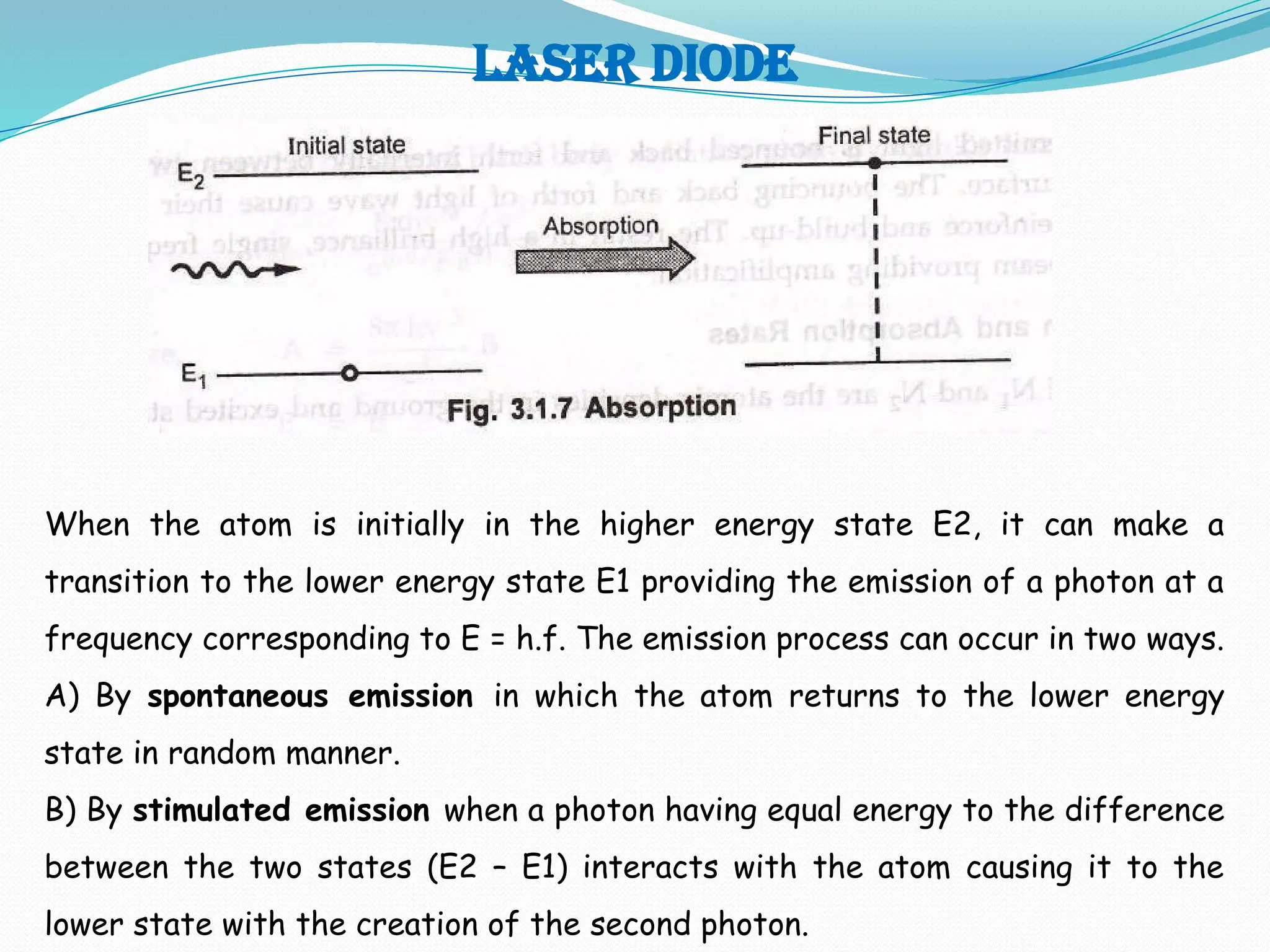
LASER DIODE
When theatom is initially in the higher energy state E2, it can make a
transition to the lower energy state E1 providing the emission of a photon at a
frequency corresponding to E = h.f. The emission process can occur in two ways.
A) By spontaneous emission in which the atom returns to the lower energy
state in random manner.
B) By stimulated emission when a photon having equal energy to the difference
between the two states (E2 – E1) interacts with the atom causing it to the
lower state with the creation of the second photon.
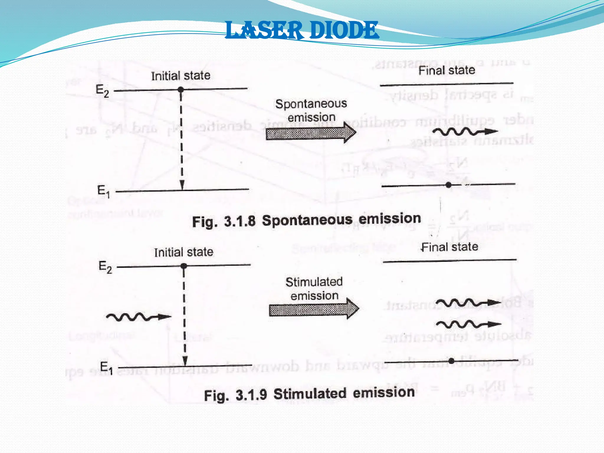
LASER DIODE
•Spontaneous emissiongives incoherent radiation while stimulated
emission gives coherent radiation. Hence the light associated with
emitted photon is of same frequency of incident photon, and in same
phase with same polarization.
•It means that when an atom is stimulated to emit light energy by an
incident wave, the liberated energy can add to the wave in constructive
manner. The emitted light is bounced back and forth internally between
two reflecting surface. The bouncing back and forth of light wave cause
their intensity to reinforce and build-up. The result in a high brilliance,
single frequency light beam providing amplification.
43.
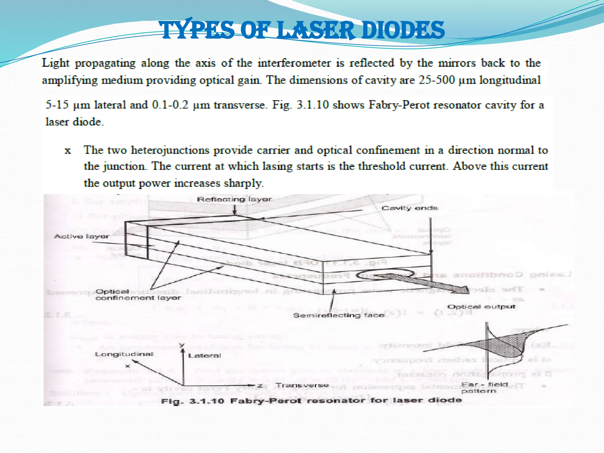
LASER DIODE MODES
In the resonant cavity of Laser Diode the Optical Radiation sets up a
pattern of EM field lines called the Model of the Cavity.
Further the Modes can be separated as
TRANSVERSE ELECTRIC
TRANSVERSE MAGNETIC
In terms of Longitudinal, Lateral and Transverse fields along the major
axis od cavity
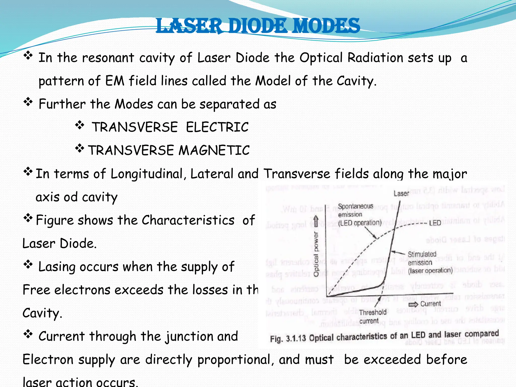
Figure shows the Characteristics of
Laser Diode.
Lasing occurs when the supply of
Free electrons exceeds the losses in the
Cavity.
Current through the junction and
Electron supply are directly proportional, and must be exceeded before
laser action occurs.
44.
LASER DIODE MODES
Laser Oscillations occur when Optical gain exceeds photon losses and this
is where Optical Gain reaches threshold gain. This is the point where
modes or resonant frequencies resonate within the cavity.
The Polished cavity ends are not perfectly reflecting with
approximately 32 % transmitting out of cleaved ends.
The Number of Modes that exist in the Output Spectrum and their
magnitudes depend on the diode current.
Longitudinal Modes : are related to the length L of the cavity It
determines the principal structures of frequency spectrum of the emitted
Optical radiation has 1 > > λ many longitudinal modes can exist.
Lateral Modes : depends on the sides of the cavity. They determine the
shape of the cavity and lateral profile of the Laser beam.
Transverse Mode : they are associated with the EM field and beam
profile in the direction perpendicular to the plane of PN junction. They
determine the Radiation pattern and Threshold current density.
45.
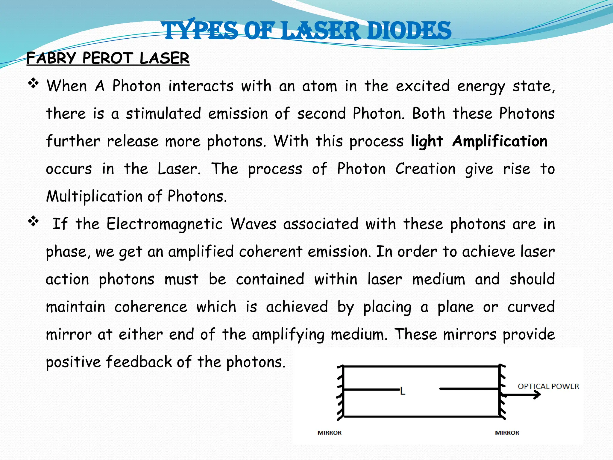
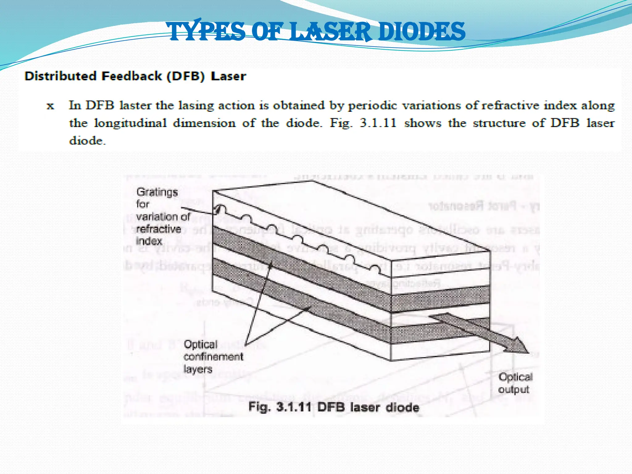
TYPES OF LASERDIODES
FABRY PEROT LASER
When A Photon interacts with an atom in the excited energy state,
there is a stimulated emission of second Photon. Both these Photons
further release more photons. With this process light Amplification
occurs in the Laser. The process of Photon Creation give rise to
Multiplication of Photons.
If the Electromagnetic Waves associated with these photons are in
phase, we get an amplified coherent emission. In order to achieve laser
action photons must be contained within laser medium and should
maintain coherence which is achieved by placing a plane or curved
mirror at either end of the amplifying medium. These mirrors provide
positive feedback of the photons.
46.
TYPES OF LASERDIODES
The photons are reflected at the mirrors at either end of the cavity
which makes the optical cavity as Oscillator rather than Amplifier with
the mirrors optical signal is feedback many times as it passes through
the medium.
Optical losses in the cavity are compensated using a gain mechanism.
The laser cavity has many resonant frequencies.
The device can oscillate at these resonant frequencies which have
sufficient gain to overcome the optical losses.
Lasing effect means that stimulated emission is the major form of
producing light in the structure this requires
Intense Charge Density
Direct Band Gap Material - > Enough Light Produced
Stimulated Emission
For Single Mode Operation the Optical Output of a Laser Diode should
contain only one Longitudinal and one Transverse mode.
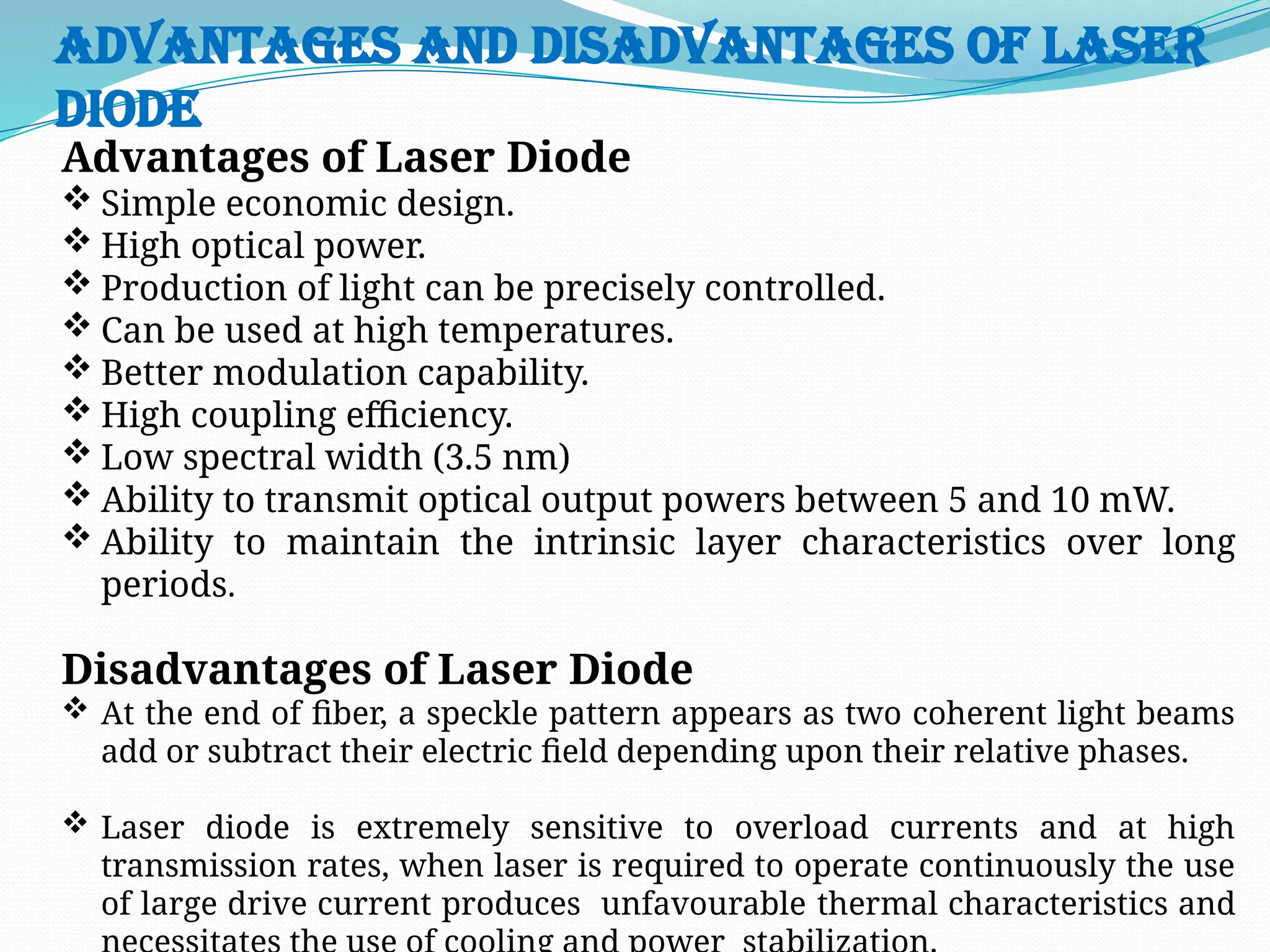
Advantages and Disadvantagesof Laser
Diode
Advantages of Laser Diode
Simple economic design.
High optical power.
Production of light can be precisely controlled.
Can be used at high temperatures.
Better modulation capability.
High coupling efficiency.
Low spectral width (3.5 nm)
Ability to transmit optical output powers between 5 and 10 mW.
Ability to maintain the intrinsic layer characteristics over long
periods.
Disadvantages of Laser Diode
At the end of fiber, a speckle pattern appears as two coherent light beams
add or subtract their electric field depending upon their relative phases.
Laser diode is extremely sensitive to overload currents and at high
transmission rates, when laser is required to operate continuously the use
of large drive current produces unfavourable thermal characteristics and
Photo Detectors
In OFCsystem it is required to convert the optical
signal at the receiver back into the electrical
signal
This task is performed by Photo Detectors
The performance of an optical detector can be
determined by its ability to detect smallest optical
power possible to generate electric power with an
absolute distortion
52.
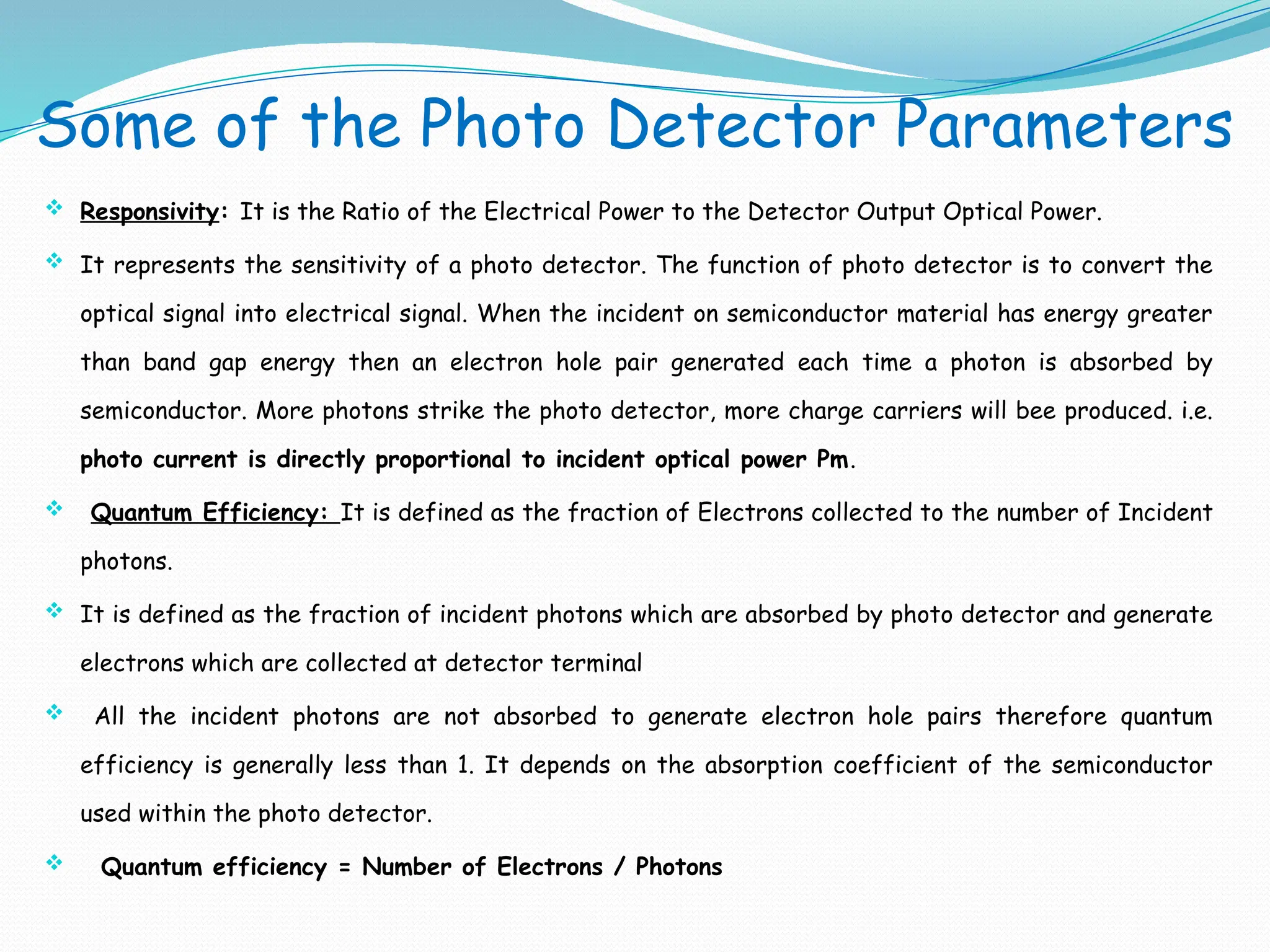
Some of thePhoto Detector Parameters
Responsivity: It is the Ratio of the Electrical Power to the Detector Output Optical Power.
It represents the sensitivity of a photo detector. The function of photo detector is to convert the
optical signal into electrical signal. When the incident on semiconductor material has energy greater
than band gap energy then an electron hole pair generated each time a photon is absorbed by
semiconductor. More photons strike the photo detector, more charge carriers will bee produced. i.e.
photo current is directly proportional to incident optical power Pm.
Quantum Efficiency: It is defined as the fraction of Electrons collected to the number of Incident
photons.
It is defined as the fraction of incident photons which are absorbed by photo detector and generate
electrons which are collected at detector terminal
All the incident photons are not absorbed to generate electron hole pairs therefore quantum
efficiency is generally less than 1. It depends on the absorption coefficient of the semiconductor
used within the photo detector.
Quantum efficiency = Number of Electrons / Photons
53.
Some of thePhoto Detector Parameters
Dark Current : The amount of current generated by the detector with no light
applied.
Dark current increases about 10% for each temperature increase of 1o
C and is much
prominent in Ge and InGaAs at longer wavelength than in Silicon at shorter wavelength.
Noise Floor: Minimum detector power that a detector can handle. The noise floor is
related to dark current since the dark current will set the lower limit.
Response Time : It is the time required for the detector to respond to an optical
Input.
The response time is related to the bandwidth of the detector BW = 0.35 /tr.
Where tr is the rise time of the device.
The rise time is the time required for the detector to rise to a value equal to 63.2 % of
its final steady state reading.
54.
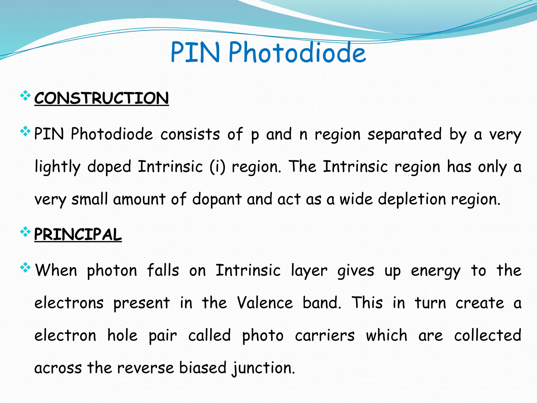
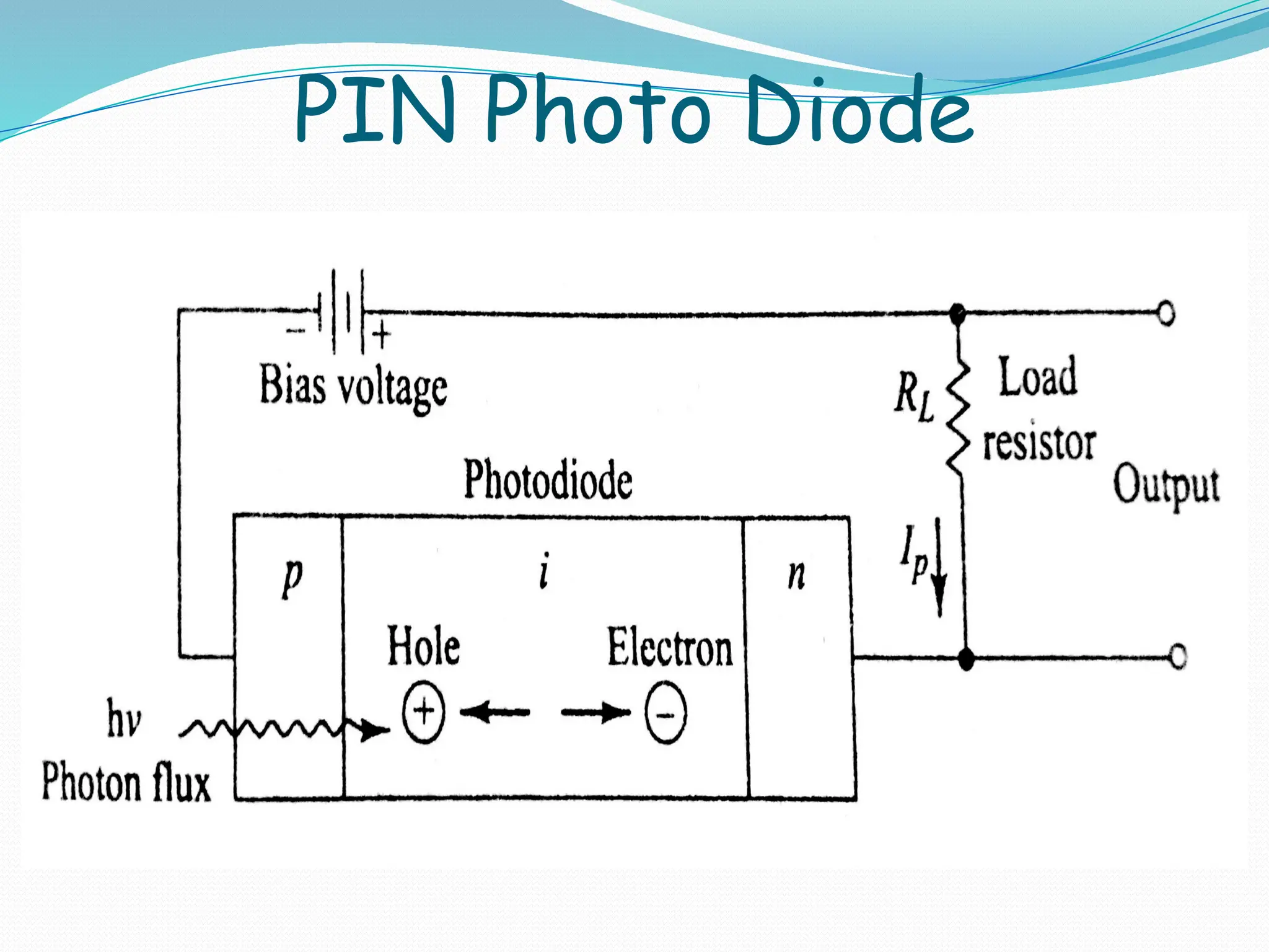
PIN Photodiode
CONSTRUCTION
PIN Photodiodeconsists of p and n region separated by a very
lightly doped Intrinsic (i) region. The Intrinsic region has only a
very small amount of dopant and act as a wide depletion region.
PRINCIPAL
When photon falls on Intrinsic layer gives up energy to the
electrons present in the Valence band. This in turn create a
electron hole pair called photo carriers which are collected
across the reverse biased junction.
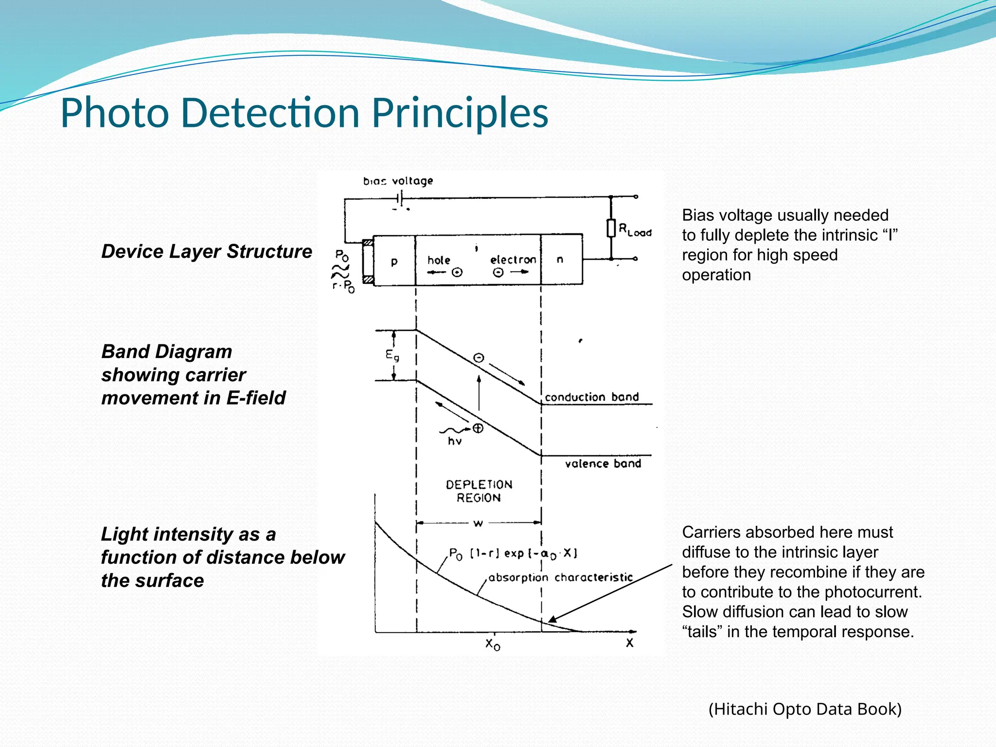
Photo Detection Principles
(HitachiOpto Data Book)
Device Layer Structure
Band Diagram
showing carrier
movement in E-field
Light intensity as a
function of distance below
the surface
Carriers absorbed here must
diffuse to the intrinsic layer
before they recombine if they are
to contribute to the photocurrent.
Slow diffusion can lead to slow
“tails” in the temporal response.
Bias voltage usually needed
to fully deplete the intrinsic “I”
region for high speed
operation
57.
PIN Photo DiodeContinued
Working:
When the incident photon has energy greater than the band gap energy of
its semiconductor material the photon can give up its energy and excite an
electron from valence band to conduction band. This process generates free
electron hole pairs known as photo carriers.
The high electric field present in the depletion region causes the carriers
to separated and be collected across the reverse bias junction. This give
rise to a current flow in an external circuit known as photo current.
Due to reverse biasing a thick depletion layer developed on either side of
the junction. The large potential barrier across the depletion layer prevent
the majority carriers. Suppose a photon of light is incident in or near the
depletion region.
58.
PIN Photo DiodeContinued
Working:
If the incident photon has energy hv equal to or greater than the band gap
energy Eg of the semiconductor material the photon will excite an electron
from valence band to conduction band. This process is called photo
generation.
The photo generated electron- hole pairs are separated in the depletion layer
are swept away by the electric field due to the applied reverse biased
voltage.
Two Important characteristics of photo detectors are
Quantum Efficiency : number of e-h pair generated / number of
incident photons = Ip / Po
Response Time

![problems
Prob 1 : The radiative and non radiative recombination life times of
minority carriers in the active region of a double heterojunction LED
are 60 nsec and 90 nsec respectively. Determine the total carrier
recombination life time and optical power generated internally if the
peak emission wavelength si 870 nm and the drive currect is 40 mA.
[July/Aug.-2006, 6 Marks]
Prob 2:A double heterjunciton InGaAsP LED operating at 1310 nm has
radiative and non-radiative recombination times of 30 and 100 ns
respectively. The current injected is 40 Ma. Calculate –
i) Bulk recombination life time.
ii) Internal quantum efficiency.
iii) Internal power level.](https://image.slidesharecdn.com/module51-251204103621-b9875a76/75/Module_5_1-pptxsatellite-and-optical-communication-36-2048.jpg)