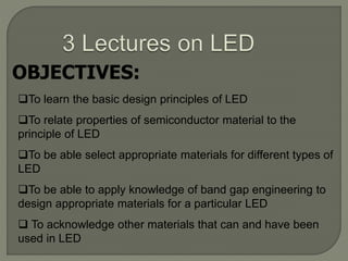
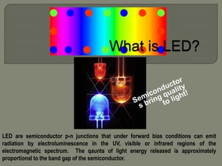
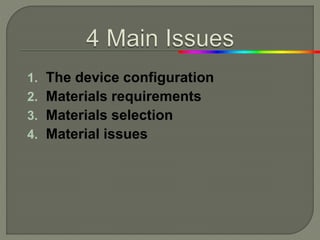
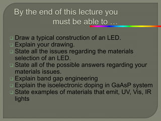
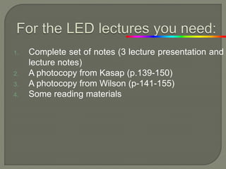
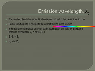
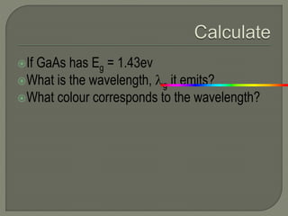
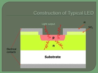
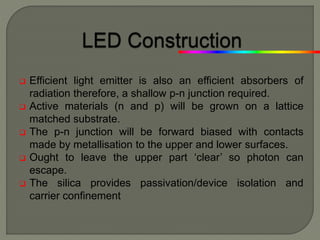
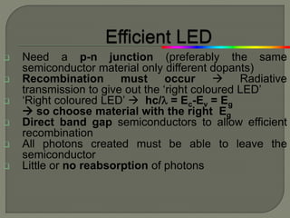
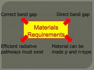
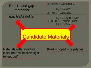
Submitted To Submitted By
www.pptplanet.com www.pptplanet.com
 Objectives
 What is LED?
 4 Main Issues
 By the end of this lecture you must be able to …
 For the LED lectures you need:
 Construction of Typical LED
 Injection Luminescence in LED
 LED Construction
 References
OBJECTIVES:
To learn the basic design principles of LED
To relate properties of semiconductor material to the
principle of LED
To be able select appropriate materials for different types of
LED
To be able to apply knowledge of band gap engineering to
design appropriate materials for a particular LED
 To acknowledge other materials that can and have been
used in LED
LED are semiconductor p-n junctions that under forward bias conditions can emit
radiation by electroluminescence in the UV, visible or infrared regions of the
electromagnetic spectrum. The qaunta of light energy released is approximately
proportional to the band gap of the semiconductor.
H.J. Round, Electrical World, 49, 309, 1907
On applying a potential to
a crystal of carborundum
(SiC), the material gave
out a yellowish light
1. The device configuration
2. Materials requirements
3. Materials selection
4. Material issues
 Draw a typical construction of an LED.
 Explain your drawing.
 State all the issues regarding the materials
selection of an LED.
 State all of the possible answers regarding your
materials issues.
 Explain band gap engineering
 Explain the isoelectronic doping in GaAsP system
 State examples of materials that emit, UV, Vis, IR
lights
1. Complete set of notes (3 lecture presentation and
lecture notes)
2. A photocopy from Kasap (p.139-150)
3. A photocopy from Wilson (p-141-155)
4. Some reading materials
Advantages of Light Emitting Diodes (LEDs)
Longevity:
The light emitting element in a diode is a small
conductor chip rather than a filament which greatly
extends the diode’s life in comparison to an
incandescent bulb (10 000 hours life time compared
to ~1000 hours for incandescence light bulb)
Efficiency:
Diodes emit almost no heat and run at very low
amperes.
Greater Light Intensity:
Since each diode emits its own light
Cost:
Not too bad
Robustness:
Solid state component, not as fragile as
incandescence light bulb
LED chip is the part
that we shall deal
with in this course
 Luminescence is a term used to describe the
emission of radiation from a solid when the
solid is supplied with some form of energy.
 Electroluminescence  excitation results from
the application of an electric field
 In a p-n junction diode injection
electroluminescence occurs resulting in light
emission when the junction is forward biased
P-n junction Electrical
Contacts
A typical LED needs a p-n junction
Junction is biased to produce even more
e-h and to inject electrons from n to p for
recombination to happen
There are a lot of electrons and holes at
the junction due to excitations
Electrons from n need to be injected to p
to promote recombination
Recombination
produces light!!
 Under forward bias – majority carriers from both sides of the junction
can cross the depletion region and entering the material at the other
side.
 Upon entering, the majority carriers become minority carriers
 For example, electrons in n-type (majority carriers) enter the p-type
to become minority carriers
 The minority carriers will be larger  minority carrier injection
 Minority carriers will diffuse and recombine with the majority carrier.
 For example, the electrons as minority carriers in the p-region will
recombine with the holes. Holes are the majority carrier in the p-
region.
 The recombination causes light to be emitted
 Such process is termed radiative recombination.
eVo
Eg
p n+
h =Eg
Eg
p n+
(a) (b)
Electrons in CB
Holes in VB
EC
EV
EF
◘Ideal LED will have all injection electrons to take part in the recombination process
◘In real device not all electron will recombine with holes to radiate light
◘Sometimes recombination occurs but no light is being emitted (non-radiative)
◘Efficiency of the device therefore can be described
◘Efficiency is the rate of photon emission over the rate of supply electrons
◘ The number of radiative recombination is proportional to the carrier injection rate
◘ Carrier injection rate is related to the current flowing in the junction
◘ If the transition take place between states (conduction and valance bands) the
emission wavelength, g = hc/(EC-EV)
◘ EC-EV = Eg
◘ g = hc/Eg
If GaAs has Eg = 1.43ev
What is the wavelength, g it emits?
What colour corresponds to the wavelength?
Substrate
n
Al
SiO2
Electrical
contacts
p
Light output
 Efficient light emitter is also an efficient absorbers of
radiation therefore, a shallow p-n junction required.
 Active materials (n and p) will be grown on a lattice
matched substrate.
 The p-n junction will be forward biased with contacts
made by metallisation to the upper and lower surfaces.
 Ought to leave the upper part ‘clear’ so photon can
escape.
 The silica provides passivation/device isolation and
carrier confinement
 Need a p-n junction (preferably the same
semiconductor material only different dopants)
 Recombination must occur  Radiative
transmission to give out the ‘right coloured LED’
 ‘Right coloured LED’  hc/ = Ec-Ev = Eg
 so choose material with the right Eg
 Direct band gap semiconductors to allow efficient
recombination
 All photons created must be able to leave the
semiconductor
 Little or no reabsorption of photons
Correct band gap Direct band gap
Material can be
made p and n-type
Efficient radiative
pathways must exist
Direct band gap
materials
e.g. GaAs not Si
 UV-ED  ~0.5-400nm
Eg > 3.25eV
 LED -  ~450-650nm
Eg = 3.1eV to 1.6eV
 IR-ED-  ~750nm- 1nm
Eg = 1.65eV
Readily doped n or p-typesMaterials with refractive
index that could allow light
to ‘get out’
Describe the principles of operation of an
LED and state the material’s requirements
criteria to produce an efficient LED.
(50 marks)
www.google.com
www.wikipedia.com
www.studymafia.org
www.pptplanet.com
www.pdfclass.com
Tech led ppt(pptplanet.com)

Tech led ppt(pptplanet.com)

  • 1.
    Submitted To SubmittedBy www.pptplanet.com www.pptplanet.com
  • 2.
     Objectives  Whatis LED?  4 Main Issues  By the end of this lecture you must be able to …  For the LED lectures you need:  Construction of Typical LED  Injection Luminescence in LED  LED Construction  References
  • 3.
    OBJECTIVES: To learn thebasic design principles of LED To relate properties of semiconductor material to the principle of LED To be able select appropriate materials for different types of LED To be able to apply knowledge of band gap engineering to design appropriate materials for a particular LED  To acknowledge other materials that can and have been used in LED
  • 4.
    LED are semiconductorp-n junctions that under forward bias conditions can emit radiation by electroluminescence in the UV, visible or infrared regions of the electromagnetic spectrum. The qaunta of light energy released is approximately proportional to the band gap of the semiconductor.
  • 5.
    H.J. Round, ElectricalWorld, 49, 309, 1907 On applying a potential to a crystal of carborundum (SiC), the material gave out a yellowish light
  • 6.
    1. The deviceconfiguration 2. Materials requirements 3. Materials selection 4. Material issues
  • 7.
     Draw atypical construction of an LED.  Explain your drawing.  State all the issues regarding the materials selection of an LED.  State all of the possible answers regarding your materials issues.  Explain band gap engineering  Explain the isoelectronic doping in GaAsP system  State examples of materials that emit, UV, Vis, IR lights
  • 8.
    1. Complete setof notes (3 lecture presentation and lecture notes) 2. A photocopy from Kasap (p.139-150) 3. A photocopy from Wilson (p-141-155) 4. Some reading materials
  • 11.
    Advantages of LightEmitting Diodes (LEDs) Longevity: The light emitting element in a diode is a small conductor chip rather than a filament which greatly extends the diode’s life in comparison to an incandescent bulb (10 000 hours life time compared to ~1000 hours for incandescence light bulb) Efficiency: Diodes emit almost no heat and run at very low amperes. Greater Light Intensity: Since each diode emits its own light Cost: Not too bad Robustness: Solid state component, not as fragile as incandescence light bulb
  • 12.
    LED chip isthe part that we shall deal with in this course
  • 13.
     Luminescence isa term used to describe the emission of radiation from a solid when the solid is supplied with some form of energy.  Electroluminescence  excitation results from the application of an electric field  In a p-n junction diode injection electroluminescence occurs resulting in light emission when the junction is forward biased
  • 14.
    P-n junction Electrical Contacts Atypical LED needs a p-n junction Junction is biased to produce even more e-h and to inject electrons from n to p for recombination to happen There are a lot of electrons and holes at the junction due to excitations Electrons from n need to be injected to p to promote recombination Recombination produces light!!
  • 15.
     Under forwardbias – majority carriers from both sides of the junction can cross the depletion region and entering the material at the other side.  Upon entering, the majority carriers become minority carriers  For example, electrons in n-type (majority carriers) enter the p-type to become minority carriers  The minority carriers will be larger  minority carrier injection  Minority carriers will diffuse and recombine with the majority carrier.  For example, the electrons as minority carriers in the p-region will recombine with the holes. Holes are the majority carrier in the p- region.  The recombination causes light to be emitted  Such process is termed radiative recombination.
  • 16.
    eVo Eg p n+ h =Eg Eg pn+ (a) (b) Electrons in CB Holes in VB EC EV EF ◘Ideal LED will have all injection electrons to take part in the recombination process ◘In real device not all electron will recombine with holes to radiate light ◘Sometimes recombination occurs but no light is being emitted (non-radiative) ◘Efficiency of the device therefore can be described ◘Efficiency is the rate of photon emission over the rate of supply electrons
  • 17.
    ◘ The numberof radiative recombination is proportional to the carrier injection rate ◘ Carrier injection rate is related to the current flowing in the junction ◘ If the transition take place between states (conduction and valance bands) the emission wavelength, g = hc/(EC-EV) ◘ EC-EV = Eg ◘ g = hc/Eg
  • 18.
    If GaAs hasEg = 1.43ev What is the wavelength, g it emits? What colour corresponds to the wavelength?
  • 19.
  • 20.
     Efficient lightemitter is also an efficient absorbers of radiation therefore, a shallow p-n junction required.  Active materials (n and p) will be grown on a lattice matched substrate.  The p-n junction will be forward biased with contacts made by metallisation to the upper and lower surfaces.  Ought to leave the upper part ‘clear’ so photon can escape.  The silica provides passivation/device isolation and carrier confinement
  • 21.
     Need ap-n junction (preferably the same semiconductor material only different dopants)  Recombination must occur  Radiative transmission to give out the ‘right coloured LED’  ‘Right coloured LED’  hc/ = Ec-Ev = Eg  so choose material with the right Eg  Direct band gap semiconductors to allow efficient recombination  All photons created must be able to leave the semiconductor  Little or no reabsorption of photons
  • 22.
    Correct band gapDirect band gap Material can be made p and n-type Efficient radiative pathways must exist
  • 23.
    Direct band gap materials e.g.GaAs not Si  UV-ED  ~0.5-400nm Eg > 3.25eV  LED -  ~450-650nm Eg = 3.1eV to 1.6eV  IR-ED-  ~750nm- 1nm Eg = 1.65eV Readily doped n or p-typesMaterials with refractive index that could allow light to ‘get out’
  • 24.
    Describe the principlesof operation of an LED and state the material’s requirements criteria to produce an efficient LED. (50 marks)
  • 25.

Editor's Notes

  • #23 Dr Zainovia Lockman L2