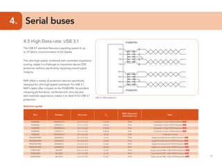
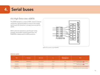
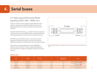
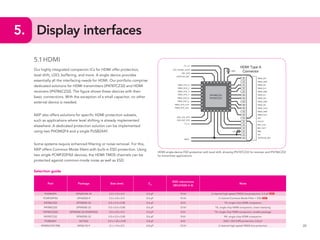
Download as PDF, PPTX
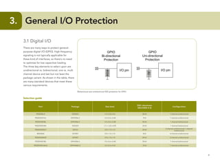
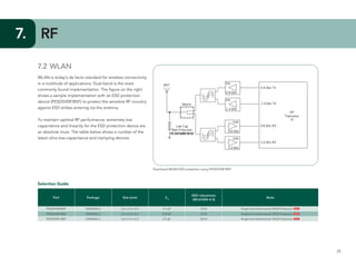


This document provides guidelines for protecting commonly used interfaces from electrostatic discharge (ESD) and transient voltages. It discusses ESD protection considerations and solutions for automotive interfaces like CAN, LIN, and FlexRay. It also covers general input/output, serial buses, displays, Ethernet, and radio frequency interfaces. For each interface, example protection circuits are shown along with NXP's recommended protection devices that offer high ESD robustness and minimal impact on signal integrity.