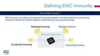
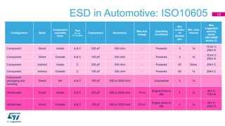
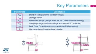
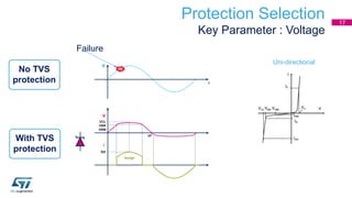
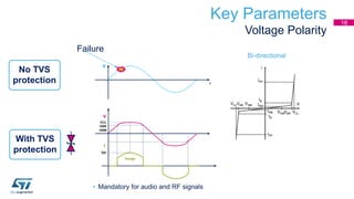
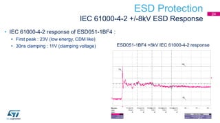
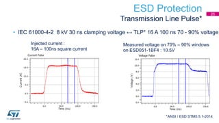
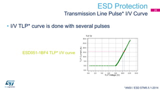
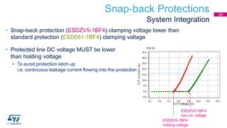
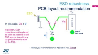
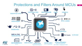
EMC - System Immunity against
Electrostatic Discharges
Mathieu ROUVIERE
Vladimir JANOUSEK
Mohamed SAADNA
Introduction
Defining EMC Immunity
EMC Immunity is the ability of an equipment to properly operate in its electromagnetic environment by
limiting the interference of electromagnetic energy that may cause physical damage.
What is EMC immunity ?
Electronic application
Radiated emissionRadiated immunity
Conducted emissionConducted immunity
3
EMC Immunity Example
Discovery Kit: STM32MP157A-DK1
USB Type-C Power Delivery
ESDA7P120-1U1M, ESDA25L
CC1, CC2VBUS
AUDIO
ESDA6V1BC6: 4-line ESD protection
OUTA, OUTB, MIC IN
USB HOST x2 (Dual USB Type-A)
ESDA7P120-1U1M (x2), ECMF02-2AMX6 (x2)
VBUS DP, DM
USB Type-C DRP (Source Only)
ESDA7P120-1U1M, ESDA25L, ECMF02-2AMX6
CC1, CC2VBUS
USB HOST x2 (Dual USB Type-A)
ESDA7P120-1U1M (x2), ECMF02-2AMX6 (x2)
VBUS DP, DM
DP, DM
HDMI
ECMF04-4HSWM10 (x2), ESDALC6V1-5M6
CEC, I2C, HPDTMDS datalines
MORPHO CONNECTOR
ESDA7P120-1U1M
5V Vin
USER BUTTONS
ESDALC6V1-1U2
MICRO SD CARD
HSP051-4M10 (x2)
SDMMC dataline
ST-LINK USB CONNECTOR
USBLC6-2P6
ETHERNET
HSP053-4M5
DP, DM, VBUS
4
AGENDA
• ESD Protection at System Level
• How to select an ESD protection device?
• ESD Layout Guidelines
• Application Examples
5
ESD Protection at System Level
Source: https://www.esda.org/about-esd/esd-fundamentals/part-1-an-introduction-to-esd/
How ESD is Generated ? 7
ESD Damages to ICs
White Paper on Electrical Overstress - EOS Industry Council on ESD Target Levels
In preparation for this white paper, the Industry Council conducted a worldwide survey of the electronics industry concerning EOS. Results
confirmed the long held view that EOS is consistently one of the “high bars” on product failure Pareto charts. Looking at the EOS survey,
respondents reported greater than 20% of total failures being EOS-related or 30% of total electrical failures being EOS-related, making
EOS the largest bar on the Pareto chart of that responder’s known causes of returns.
Source:https://pdfs.semanticscholar.org/235b/0bfd01dd5f0c6c2c99df3b93bc27f56a9cfd.pdf
“30% of total electrical failure is EOS -related”
Silicon melting Hole in the oxide Melting Flash
Source: STMicroelectronics
8
ESD Sensitivity is Increasing
Vdd = power supply voltage
VBD = breakdown voltage
V
2V
8V
9
ESD and EOS Standards
ESD and EOS standards
ESD
Electro-Static Discharge
EOS
Electrical Over
Stress
Component level
to ensure manufacturability
System level
to assure
robustness
HBM
Human Body
Model
CDM
Charged Device
model
MM
Machine Model
ISO7637
ISO16750
IEC 61000-4-2
ISO10605 (auto)
Final user simulation
System robustness for end users. Uncontrolled environment.These standards have low-level surges as factories are well-controlled environments.
System level
to simulate car
behavior
10
Energy for 8kV IEC 61000-4-2
Energy for 8kV HBM
Energy for 2kV HBM
HV
supply
R(MΩ) 1500Ω
DUT
100pF
Human Body Model for IC
(+/-2kV for most of IC)
HV
supply
R(MΩ) 330Ω
DUT
150pF
IEC 61000-4-2 for system
(+/-8kV for level 4)
HBM and IEC Standards 11
Difference in standards : IEC 61000-4-2 carries more energy than HBM
Silicon die area for
component level ESD
(2 kV HBM)
Silicon die area for
system level ESD
(8 kV IEC contact)
Component Level vs System Level
Silicon Die Area Comparison
12
System-level ESD protection standard
IEC 61000-4-2 test bench
Contact discharge Air discharge
Stress Level
Test Voltage (kV) Test Voltage (kV) Number of
dischargeq
1 2 4 At least 10 single
discharges at 1 Hz
in the most
sensitive polarity
2 4 6
3 6 8
4 8 15
System state as a result of system–level ESD stress
A Normal performance
B
Temporary loss of function or degradation of performance which
cease after the disturbance ceases. The DUT recover its normal
performance , without operator intervention
C Temporary loss of function or degradation of performance , the
correction of which requires operator intervention
D loss of function or degradation of performance, no recovery possible
Self-restored
Require a system reset
13
ESD in Automotive: ISO10605
Configuration Mode
Component
acessible
from:
Test
(A= Air
C= contact)
Capacitance Resistance
Max test
voltage
Operating
conditions
Min
number
of
dischar
ges
Min. time
interval
Max
suggested
severity
levels
(ISO10605
Annex C)
Component Direct Inside A & C 330 pF 330 ohm - Powered 3 1s
15 kV C
25kV A
Component Direct Outside A & C 150 pF 330 ohm - Powered 3 1s
15 kV C
25kV A
Component Indirect Inside C 330 pF 330 ohm - Powered 50 50ms 20kV C
Component Indirect Outside C 150 pF 330 ohm - Powered 50 1s 20kV C
Component
packaging and
handling
Direct NA A & C 150 pF 330 or 2000 ohm - Unpowered 3 1s
Vehicle test Direct Inside A & C 330 pF 330 or 2000 ohm 15 kV
Engine drive or
idle
3 1s
8kV C
15kV A
Vehicle test Direct Outside A & C 150 pF 330 or 2000 ohm 25 kV
Engine drive or
idle
3 1s
8kV C
25kV A
14
How to Select ESD Protection Device
Key Parameters
Parameters Description
VRM Stand-off voltage (normal condition voltage)
IRM Leakage current
VBR Breakdown voltage (voltage when the ESD protection starts working)
VCL Clamping voltage (maximum voltage accross the ESD protection)
IPP Peak Pulse Current (maximum current in the ESD protection)
C Line capacitance (impacts signal integrity)
16
Protection Selection
Key Parameter : Voltage
VBR
Isurge
VF
Ipp
V
No TVS
protection
Failure
VCL
t
VRM
V
Uni-directional
I
With TVS
protection
17
• Mandatory for audio and RF signals
Bi-directional
VBR
Isurge
Ipp
V
Failure
VCL
t
VRM
V
I
No TVS
protection
With TVS
protection
Key Parameters
Voltage Polarity
18
Time domain Frequency domain
Key Parameters
Capacitance Value
• Example of the impact of parasitic capacitance on high-speed signal
simulated with discrete capacitance
19
Fc =
1
π tr
fc
240 MHz
S21 (dB)V
Eye Diagram
What is an Eye Diagram?
1 0 1
0 1 0
0 1 1
1 1 0
0 0 1
1 0 0
0 0 0
1 1 1
0 0 0
0 0 1
0 1 0
0 1 1
1 0 0
1 0 1
1 1 0
1 1 1
20
Impact on Data-lines
Eye Diagram Integrity
• USB 3.1 Gen2 mask at 10.0 Gbps per channel
(Type-C connector, reference cable, EQ with DC=6dB and DFE)
21
Line without HSP053-4M5 Line with HSP053-4M5
Impact on Data-lines
Time Domain Reflectometer Impedance
TDR with 200ps pule rise time impedance of
100Ω line without / with HSP053-4M5
ZLOAD
Step
generator
50Ω
Z0
Transmission Line
Oscilloscope Mainframe
Sampler
ZLOAD
Step
generator
50Ω
Z0
Transmission Line
Oscilloscope Mainframe
Sampler
Step
generator
50Ω
Z0
Transmission Line
Oscilloscope Mainframe
Sampler
HDMI 2.0b TDR specification : 100Ω ±15Ω
Incident step Reflected step
TDR voltage
22
Impact on RF-signal
S21 Attenuation
• ESDARF02-1BU2CK S21
• 30 GHz at -3 dB
• 8 GHz at -0.5 dB
• Negligible impact major frequencies for telecom
• FM radio : 87.5 MHz - 108.0 MHz
• Numerical TV : 400 MHz – 900 MHz
• Cellular phones : 700 MHz … 4.7 GHz
• GNSS : 1.6 GHz
• Bluetooth : 2.4 GHz
• Sub-GHz industrial : 400 MHz … 1.1GHz
• WiFi : 2.4 / 5.0 GHz
10M 100M 1G 10G 100G
-4
-3.5
-3
-2.5
-2
-1.5
-1
-0.5
0
ESDARF02-1BU2CK
APLAC 8.21 User: F:Cust# 8463:STMicroelectronics Tours SAS:National Instruments
f/Hz
ESDARF02-1BU2C
23
ESD Protection
IEC 61000-4-2 +/-8kV ESD Response
• IEC 61000-4-2 response of ESD051-1BF4 :
• First peak : 23V (low energy, CDM like)
• 30ns clamping : 11V (clamping voltage) ESD051-1BF4 +8kV IEC 61000-4-2 response
24
ESD Protection
Transmission Line Pulse*
• IEC 61000-4-2 8 kV 30 ns clamping voltage ↔ TLP* 16 A 100 ns 70 - 90% voltage
Injected current :
16A – 100ns square current
Measured voltage on 70% – 90% windows
on ESD051-1BF4 : 10.5V
*ANSI / ESD STM5.5.1-2014
25
ESD Protection
Transmission Line Pulse* I/V Curve
• I/V TLP* curve is done with several pulses
*ANSI / ESD STM5.5.1-2014
ESD051-1BF4 TLP* I/V curve
26
System-Efficient ESD
Design Methodology
• TLP input current shared between high performance MCU FT input and ESDA5-1BF4
• High performance MCU + ESDA5-1BF4 robustness reach more than 8kV IEC 61000-4-2
• Even if, ESD5-1BF4 clamping voltage > High Performance MCU FT input AMR
• ESD051-1BF4
• 11V clamping voltage at +8kV ESD 61000-4-2
• High Performance MCU FT input
• 3.6 V max operating
• 2 kV HBM ESD
• 250 V CMD ESD
• 5.5 V AMR
MCU working voltage : 3.3V
MCU destruction voltage : 12.5V
27
Snap-back Protections
System Integration
• Snap-back protection (ESDZV5-1BF4) clamping voltage lower than
standard protection (ESD051-1BF4) clamping voltage
• Protected line DC voltage MUST be lower
than holding voltage
• To avoid protection latch-up
i.e. continuous leakage current flowing into the protection
ESDZV5-1BF4
holding voltage
ESDZV5-1BF4
turn-on voltage
28
Recap
Basics of ESD Protection
• Transparency :
• Capacitance must be in-line with application bandwidth / data rate
• Efficiency :
• VRM must be slightly higher than maximum line voltage
To obtain a low clamping voltage
• System integration of snap-back protection :
• Holding voltage must be higher than DC voltage
10M 100M 1G 10G 100G
-4
-3.5
-3
-2.5
-2
-1.5
-1
-0.5
0
ESDARF02-1BU2CK
APLAC 8.21 User: F:Cust# 8463:STMicroelectronics Tours SAS:National Instruments
f/Hz
ESDARF02-1BU2C
AN5241, Fundamentals of ESD protection at system level
29
ESD Layout Guidelines
ESD Robustness
PCB Layout Impact
• PCB Tracks must be under control !
• For protection device length
connection of ~1cm from side to
side, 35µm copper, 0.5mm wide
(microstrip)
• 2 x L = 5 nH !
31
Vcc
Vias to
GND plane
L
L
=
=
ICtoprotect
Vias to
GND plane
ESD Robustness
PCB Layout Impact
dt
di
L
V
Vic
Assuming that lines inductance
is L = 5nH
di/dt = 37.5 A / ns
Vic= V + 2 x L x di/dt
Vic= V + 375 V
ESD surge is
8 kV /0.8 ns rise time, this
makes 37.5 A/nsdt
di
L
ESD
ICtoprotect
Vias to
GND plane
Vcc
Vias to
GND plane
32
ESD Robustness
PCB Layout Recommendation
Vias to GND plane as close as possible to the product GND
ICtoprotect
Vias to
GND plane
Vcc
ESD
33
PCB Layout recommendations in Application note AN1751
Vcc
ICtoprotect
Vic
In this case, Vic ≤ V
In addition, ESD
protection must be placed
as close as possible to the
ESD source, to avoid any
coupling between tracks
on the PCB.
ESD robustness
PCB layout recommendation
V
Vias to
GND plane
ESD
34
Application Examples
Recommended Protection Devices and PCB Layouts
Protections and Filters Around MCUs 36
ECMF04-4HSWM10
High Speed Differential
MIPI, USB 3.1, Display port, HDMI
ESDALC6V1W5
ESDA6V1BC6
SPT01-335DEE
HSP051-4M10
ETH 1G, secondary
ESDA7P120-1U1M
USBLC6-2SC6
TCPP01-M12
Type-C Port Protection
EMIF06-MSD02N16
SD 2.0
EMIF03-SIM02M8 ESDA5V3LDSILC6-4P6 (TAG) SMA6F
ESDA14V2BP6
RS-232
SMAJ40CA
CLT03-2Q3PLC inputs
USB 2.0 Full Speed
Without OTG
SOD323-6L
 Compliant with USB 2.0 eye diagram
 ESD robustness: + 15 kV contact discharge IEC61000-4-2
USBLC6-2SC6
Reuse gerber file
STM32L4R9I-EVAL
DESIGN TIP:
Place the ESD protection close to ESD
source: here close to USB connector
37
RS-232
Reuse gerber file
STM32L4R9I-EVAL
 Low capacitance, 4-line, bi-directional ESD protection
 ESD protection as per IEC61000-4-2 Level 4: + 8kV contact
ESDA14V2BP6
SOT666-6L
DESIGN TIP:
Place the ESD protection close to ESD source:
here close to RS-232 connector
38
USER BUTTON
GPIO Input
SOT23-3L
 PCB space saving: 2 diodes array
 ESD robustness: + 30 kV contact discharge IEC61000-4-2
ESDA5V3L
Reuse gerber file
STM32L4R9I-EVAL
Design note:
Although buttons are not
made of conductive
materials, they are highly
sensitive to ESD air
discharge used during
IEC certification tests
39
ESD protections in STM32MP1 40
USB Type-C Power Delivery
ESDA7P120-1U1M, ESDA25L
CC1, CC2VBUS
AUDIO
ESDA6V1BC6: 4-line ESD protection
OUTA, OUTB, MIC IN
USB HOST x2 (Dual USB Type-A)
ESDA7P120-1U1M (x2), ECMF02-2AMX6 (x2)
VBUS DP, DM
USB Type-C DRP (Source Only)
ESDA7P120-1U1M, ESDA25L, ECMF02-2AMX6
CC1, CC2VBUS
USB HOST x2 (Dual USB Type-A)
ESDA7P120-1U1M (x2), ECMF02-2AMX6 (x2)
VBUS DP, DM
DP, DM
HDMI
ECMF04-4HSWM10 (x2), ESDALC6V1-5M6
CEC, I2C, HPDTMDS datalines
MORPHO CONNECTOR
ESDA7P120-1U1M
5V Vin
USER BUTTONS
ESDALC6V1-1U2
MICRO SD CARD
HSP051-4M10 (x2)
SDMMC dataline
ST-LINK USB CONNECTOR
USBLC6-2P6
ETHERNET
HSP053-4M5
DP, DM, VBUS
Any Electronic Board Must be Protected
3D-printer Control Board
41
• Protections on the application PCB
• Power lines → surge protection : IEC
61000-4-5
• Connector
• Button
• SD card
• Integrated on all IC’s → ESD protection
for manufacturing is JEDEC HBM
SMAJ12A
SMBJ24A
EMIF06-MSD02N16
3x USBLC6-2SC6
ESDA5V3L
ESD protection for
system : IEC 61000-4-2
Resources
Application Notes and Video
• AN5241, Fundamentals of ESD protection at system level
• AN4871, USB Type-C protection and filtering
• AN5121, HDMI ESD protection and signal conditioning products for STBs
• AN3353, IEC 61000-4-2 standard testing
• AN2689, Protection of automotive electronics from electrical hazards,
guidelines for design and component selection
• AN1826, TRANSIENT PROTECTION SOLUTIONS: Transil™ diode versus
Varistor
• AN5241 : Fundamentals of ESD Protection
• Video - ESD Protection: why and how to protect microcontrollers efficiently
42
ST Protection Finder Mobile App
• ST-PROTECTION-FINDER is an application available for
Android™ and iOS™ that allows you to explore ST’s TVS
product portfolio.
• Parametric or series search engine
• Efficient part number search engine
43
4 Steps to Discover ST’s Portfolio
1
OPEN
application
2
SELECT
parameter
3
CHOOSE
product
44
4
GET
datasheet
45

How to protect electronic systems against esd

  • 1.
    EMC - SystemImmunity against Electrostatic Discharges Mathieu ROUVIERE Vladimir JANOUSEK Mohamed SAADNA
  • 2.
  • 3.
    Defining EMC Immunity EMCImmunity is the ability of an equipment to properly operate in its electromagnetic environment by limiting the interference of electromagnetic energy that may cause physical damage. What is EMC immunity ? Electronic application Radiated emissionRadiated immunity Conducted emissionConducted immunity 3
  • 4.
    EMC Immunity Example DiscoveryKit: STM32MP157A-DK1 USB Type-C Power Delivery ESDA7P120-1U1M, ESDA25L CC1, CC2VBUS AUDIO ESDA6V1BC6: 4-line ESD protection OUTA, OUTB, MIC IN USB HOST x2 (Dual USB Type-A) ESDA7P120-1U1M (x2), ECMF02-2AMX6 (x2) VBUS DP, DM USB Type-C DRP (Source Only) ESDA7P120-1U1M, ESDA25L, ECMF02-2AMX6 CC1, CC2VBUS USB HOST x2 (Dual USB Type-A) ESDA7P120-1U1M (x2), ECMF02-2AMX6 (x2) VBUS DP, DM DP, DM HDMI ECMF04-4HSWM10 (x2), ESDALC6V1-5M6 CEC, I2C, HPDTMDS datalines MORPHO CONNECTOR ESDA7P120-1U1M 5V Vin USER BUTTONS ESDALC6V1-1U2 MICRO SD CARD HSP051-4M10 (x2) SDMMC dataline ST-LINK USB CONNECTOR USBLC6-2P6 ETHERNET HSP053-4M5 DP, DM, VBUS 4
  • 5.
    AGENDA • ESD Protectionat System Level • How to select an ESD protection device? • ESD Layout Guidelines • Application Examples 5
  • 6.
    ESD Protection atSystem Level
  • 7.
  • 8.
    ESD Damages toICs White Paper on Electrical Overstress - EOS Industry Council on ESD Target Levels In preparation for this white paper, the Industry Council conducted a worldwide survey of the electronics industry concerning EOS. Results confirmed the long held view that EOS is consistently one of the “high bars” on product failure Pareto charts. Looking at the EOS survey, respondents reported greater than 20% of total failures being EOS-related or 30% of total electrical failures being EOS-related, making EOS the largest bar on the Pareto chart of that responder’s known causes of returns. Source:https://pdfs.semanticscholar.org/235b/0bfd01dd5f0c6c2c99df3b93bc27f56a9cfd.pdf “30% of total electrical failure is EOS -related” Silicon melting Hole in the oxide Melting Flash Source: STMicroelectronics 8
  • 9.
    ESD Sensitivity isIncreasing Vdd = power supply voltage VBD = breakdown voltage V 2V 8V 9
  • 10.
    ESD and EOSStandards ESD and EOS standards ESD Electro-Static Discharge EOS Electrical Over Stress Component level to ensure manufacturability System level to assure robustness HBM Human Body Model CDM Charged Device model MM Machine Model ISO7637 ISO16750 IEC 61000-4-2 ISO10605 (auto) Final user simulation System robustness for end users. Uncontrolled environment.These standards have low-level surges as factories are well-controlled environments. System level to simulate car behavior 10
  • 11.
    Energy for 8kVIEC 61000-4-2 Energy for 8kV HBM Energy for 2kV HBM HV supply R(MΩ) 1500Ω DUT 100pF Human Body Model for IC (+/-2kV for most of IC) HV supply R(MΩ) 330Ω DUT 150pF IEC 61000-4-2 for system (+/-8kV for level 4) HBM and IEC Standards 11 Difference in standards : IEC 61000-4-2 carries more energy than HBM
  • 12.
    Silicon die areafor component level ESD (2 kV HBM) Silicon die area for system level ESD (8 kV IEC contact) Component Level vs System Level Silicon Die Area Comparison 12
  • 13.
    System-level ESD protectionstandard IEC 61000-4-2 test bench Contact discharge Air discharge Stress Level Test Voltage (kV) Test Voltage (kV) Number of dischargeq 1 2 4 At least 10 single discharges at 1 Hz in the most sensitive polarity 2 4 6 3 6 8 4 8 15 System state as a result of system–level ESD stress A Normal performance B Temporary loss of function or degradation of performance which cease after the disturbance ceases. The DUT recover its normal performance , without operator intervention C Temporary loss of function or degradation of performance , the correction of which requires operator intervention D loss of function or degradation of performance, no recovery possible Self-restored Require a system reset 13
  • 14.
    ESD in Automotive:ISO10605 Configuration Mode Component acessible from: Test (A= Air C= contact) Capacitance Resistance Max test voltage Operating conditions Min number of dischar ges Min. time interval Max suggested severity levels (ISO10605 Annex C) Component Direct Inside A & C 330 pF 330 ohm - Powered 3 1s 15 kV C 25kV A Component Direct Outside A & C 150 pF 330 ohm - Powered 3 1s 15 kV C 25kV A Component Indirect Inside C 330 pF 330 ohm - Powered 50 50ms 20kV C Component Indirect Outside C 150 pF 330 ohm - Powered 50 1s 20kV C Component packaging and handling Direct NA A & C 150 pF 330 or 2000 ohm - Unpowered 3 1s Vehicle test Direct Inside A & C 330 pF 330 or 2000 ohm 15 kV Engine drive or idle 3 1s 8kV C 15kV A Vehicle test Direct Outside A & C 150 pF 330 or 2000 ohm 25 kV Engine drive or idle 3 1s 8kV C 25kV A 14
  • 15.
    How to SelectESD Protection Device
  • 16.
    Key Parameters Parameters Description VRMStand-off voltage (normal condition voltage) IRM Leakage current VBR Breakdown voltage (voltage when the ESD protection starts working) VCL Clamping voltage (maximum voltage accross the ESD protection) IPP Peak Pulse Current (maximum current in the ESD protection) C Line capacitance (impacts signal integrity) 16
  • 17.
    Protection Selection Key Parameter: Voltage VBR Isurge VF Ipp V No TVS protection Failure VCL t VRM V Uni-directional I With TVS protection 17
  • 18.
    • Mandatory foraudio and RF signals Bi-directional VBR Isurge Ipp V Failure VCL t VRM V I No TVS protection With TVS protection Key Parameters Voltage Polarity 18
  • 19.
    Time domain Frequencydomain Key Parameters Capacitance Value • Example of the impact of parasitic capacitance on high-speed signal simulated with discrete capacitance 19 Fc = 1 π tr fc 240 MHz S21 (dB)V
  • 20.
    Eye Diagram What isan Eye Diagram? 1 0 1 0 1 0 0 1 1 1 1 0 0 0 1 1 0 0 0 0 0 1 1 1 0 0 0 0 0 1 0 1 0 0 1 1 1 0 0 1 0 1 1 1 0 1 1 1 20
  • 21.
    Impact on Data-lines EyeDiagram Integrity • USB 3.1 Gen2 mask at 10.0 Gbps per channel (Type-C connector, reference cable, EQ with DC=6dB and DFE) 21 Line without HSP053-4M5 Line with HSP053-4M5
  • 22.
    Impact on Data-lines TimeDomain Reflectometer Impedance TDR with 200ps pule rise time impedance of 100Ω line without / with HSP053-4M5 ZLOAD Step generator 50Ω Z0 Transmission Line Oscilloscope Mainframe Sampler ZLOAD Step generator 50Ω Z0 Transmission Line Oscilloscope Mainframe Sampler Step generator 50Ω Z0 Transmission Line Oscilloscope Mainframe Sampler HDMI 2.0b TDR specification : 100Ω ±15Ω Incident step Reflected step TDR voltage 22
  • 23.
    Impact on RF-signal S21Attenuation • ESDARF02-1BU2CK S21 • 30 GHz at -3 dB • 8 GHz at -0.5 dB • Negligible impact major frequencies for telecom • FM radio : 87.5 MHz - 108.0 MHz • Numerical TV : 400 MHz – 900 MHz • Cellular phones : 700 MHz … 4.7 GHz • GNSS : 1.6 GHz • Bluetooth : 2.4 GHz • Sub-GHz industrial : 400 MHz … 1.1GHz • WiFi : 2.4 / 5.0 GHz 10M 100M 1G 10G 100G -4 -3.5 -3 -2.5 -2 -1.5 -1 -0.5 0 ESDARF02-1BU2CK APLAC 8.21 User: F:Cust# 8463:STMicroelectronics Tours SAS:National Instruments f/Hz ESDARF02-1BU2C 23
  • 24.
    ESD Protection IEC 61000-4-2+/-8kV ESD Response • IEC 61000-4-2 response of ESD051-1BF4 : • First peak : 23V (low energy, CDM like) • 30ns clamping : 11V (clamping voltage) ESD051-1BF4 +8kV IEC 61000-4-2 response 24
  • 25.
    ESD Protection Transmission LinePulse* • IEC 61000-4-2 8 kV 30 ns clamping voltage ↔ TLP* 16 A 100 ns 70 - 90% voltage Injected current : 16A – 100ns square current Measured voltage on 70% – 90% windows on ESD051-1BF4 : 10.5V *ANSI / ESD STM5.5.1-2014 25
  • 26.
    ESD Protection Transmission LinePulse* I/V Curve • I/V TLP* curve is done with several pulses *ANSI / ESD STM5.5.1-2014 ESD051-1BF4 TLP* I/V curve 26
  • 27.
    System-Efficient ESD Design Methodology •TLP input current shared between high performance MCU FT input and ESDA5-1BF4 • High performance MCU + ESDA5-1BF4 robustness reach more than 8kV IEC 61000-4-2 • Even if, ESD5-1BF4 clamping voltage > High Performance MCU FT input AMR • ESD051-1BF4 • 11V clamping voltage at +8kV ESD 61000-4-2 • High Performance MCU FT input • 3.6 V max operating • 2 kV HBM ESD • 250 V CMD ESD • 5.5 V AMR MCU working voltage : 3.3V MCU destruction voltage : 12.5V 27
  • 28.
    Snap-back Protections System Integration •Snap-back protection (ESDZV5-1BF4) clamping voltage lower than standard protection (ESD051-1BF4) clamping voltage • Protected line DC voltage MUST be lower than holding voltage • To avoid protection latch-up i.e. continuous leakage current flowing into the protection ESDZV5-1BF4 holding voltage ESDZV5-1BF4 turn-on voltage 28
  • 29.
    Recap Basics of ESDProtection • Transparency : • Capacitance must be in-line with application bandwidth / data rate • Efficiency : • VRM must be slightly higher than maximum line voltage To obtain a low clamping voltage • System integration of snap-back protection : • Holding voltage must be higher than DC voltage 10M 100M 1G 10G 100G -4 -3.5 -3 -2.5 -2 -1.5 -1 -0.5 0 ESDARF02-1BU2CK APLAC 8.21 User: F:Cust# 8463:STMicroelectronics Tours SAS:National Instruments f/Hz ESDARF02-1BU2C AN5241, Fundamentals of ESD protection at system level 29
  • 30.
  • 31.
    ESD Robustness PCB LayoutImpact • PCB Tracks must be under control ! • For protection device length connection of ~1cm from side to side, 35µm copper, 0.5mm wide (microstrip) • 2 x L = 5 nH ! 31 Vcc Vias to GND plane L L = = ICtoprotect Vias to GND plane
  • 32.
    ESD Robustness PCB LayoutImpact dt di L V Vic Assuming that lines inductance is L = 5nH di/dt = 37.5 A / ns Vic= V + 2 x L x di/dt Vic= V + 375 V ESD surge is 8 kV /0.8 ns rise time, this makes 37.5 A/nsdt di L ESD ICtoprotect Vias to GND plane Vcc Vias to GND plane 32
  • 33.
    ESD Robustness PCB LayoutRecommendation Vias to GND plane as close as possible to the product GND ICtoprotect Vias to GND plane Vcc ESD 33
  • 34.
    PCB Layout recommendationsin Application note AN1751 Vcc ICtoprotect Vic In this case, Vic ≤ V In addition, ESD protection must be placed as close as possible to the ESD source, to avoid any coupling between tracks on the PCB. ESD robustness PCB layout recommendation V Vias to GND plane ESD 34
  • 35.
  • 36.
    Protections and FiltersAround MCUs 36 ECMF04-4HSWM10 High Speed Differential MIPI, USB 3.1, Display port, HDMI ESDALC6V1W5 ESDA6V1BC6 SPT01-335DEE HSP051-4M10 ETH 1G, secondary ESDA7P120-1U1M USBLC6-2SC6 TCPP01-M12 Type-C Port Protection EMIF06-MSD02N16 SD 2.0 EMIF03-SIM02M8 ESDA5V3LDSILC6-4P6 (TAG) SMA6F ESDA14V2BP6 RS-232 SMAJ40CA CLT03-2Q3PLC inputs
  • 37.
    USB 2.0 FullSpeed Without OTG SOD323-6L  Compliant with USB 2.0 eye diagram  ESD robustness: + 15 kV contact discharge IEC61000-4-2 USBLC6-2SC6 Reuse gerber file STM32L4R9I-EVAL DESIGN TIP: Place the ESD protection close to ESD source: here close to USB connector 37
  • 38.
    RS-232 Reuse gerber file STM32L4R9I-EVAL Low capacitance, 4-line, bi-directional ESD protection  ESD protection as per IEC61000-4-2 Level 4: + 8kV contact ESDA14V2BP6 SOT666-6L DESIGN TIP: Place the ESD protection close to ESD source: here close to RS-232 connector 38
  • 39.
    USER BUTTON GPIO Input SOT23-3L PCB space saving: 2 diodes array  ESD robustness: + 30 kV contact discharge IEC61000-4-2 ESDA5V3L Reuse gerber file STM32L4R9I-EVAL Design note: Although buttons are not made of conductive materials, they are highly sensitive to ESD air discharge used during IEC certification tests 39
  • 40.
    ESD protections inSTM32MP1 40 USB Type-C Power Delivery ESDA7P120-1U1M, ESDA25L CC1, CC2VBUS AUDIO ESDA6V1BC6: 4-line ESD protection OUTA, OUTB, MIC IN USB HOST x2 (Dual USB Type-A) ESDA7P120-1U1M (x2), ECMF02-2AMX6 (x2) VBUS DP, DM USB Type-C DRP (Source Only) ESDA7P120-1U1M, ESDA25L, ECMF02-2AMX6 CC1, CC2VBUS USB HOST x2 (Dual USB Type-A) ESDA7P120-1U1M (x2), ECMF02-2AMX6 (x2) VBUS DP, DM DP, DM HDMI ECMF04-4HSWM10 (x2), ESDALC6V1-5M6 CEC, I2C, HPDTMDS datalines MORPHO CONNECTOR ESDA7P120-1U1M 5V Vin USER BUTTONS ESDALC6V1-1U2 MICRO SD CARD HSP051-4M10 (x2) SDMMC dataline ST-LINK USB CONNECTOR USBLC6-2P6 ETHERNET HSP053-4M5 DP, DM, VBUS
  • 41.
    Any Electronic BoardMust be Protected 3D-printer Control Board 41 • Protections on the application PCB • Power lines → surge protection : IEC 61000-4-5 • Connector • Button • SD card • Integrated on all IC’s → ESD protection for manufacturing is JEDEC HBM SMAJ12A SMBJ24A EMIF06-MSD02N16 3x USBLC6-2SC6 ESDA5V3L ESD protection for system : IEC 61000-4-2
  • 42.
    Resources Application Notes andVideo • AN5241, Fundamentals of ESD protection at system level • AN4871, USB Type-C protection and filtering • AN5121, HDMI ESD protection and signal conditioning products for STBs • AN3353, IEC 61000-4-2 standard testing • AN2689, Protection of automotive electronics from electrical hazards, guidelines for design and component selection • AN1826, TRANSIENT PROTECTION SOLUTIONS: Transil™ diode versus Varistor • AN5241 : Fundamentals of ESD Protection • Video - ESD Protection: why and how to protect microcontrollers efficiently 42
  • 43.
    ST Protection FinderMobile App • ST-PROTECTION-FINDER is an application available for Android™ and iOS™ that allows you to explore ST’s TVS product portfolio. • Parametric or series search engine • Efficient part number search engine 43
  • 44.
    4 Steps toDiscover ST’s Portfolio 1 OPEN application 2 SELECT parameter 3 CHOOSE product 44 4 GET datasheet
  • 45.