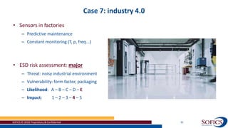
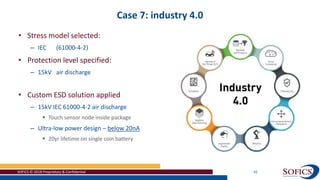
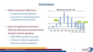
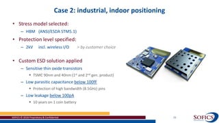
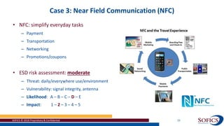
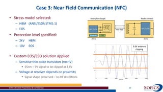
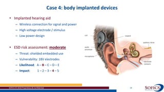
The document discusses the adequacy of 1kV for ESD protection in IoT semiconductor design, outlining the evolution of ESD standards and the challenges faced in modern applications. It analyzes risks based on various IoT applications through case studies, highlighting that while 1kV is generally sufficient under controlled conditions, specific scenarios may require higher levels of protection. The necessity for tailored ESD solutions and the importance of early design phase considerations are emphasized to address evolving threats in diverse operational environments.

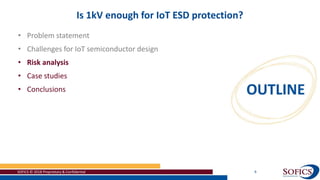
![Risk analysis – ISO 31000
SOFICS © 2018 Proprietary & Confidential 10
• Risk assesment matrix
– Identify threats
– Assess vulnerability
– Determine likelihood
– Determine impact
– Define risk and mitigation
Impact
RISK
Negligible
[1]
Minor
[2]
Serious
[3]
Critical
[4]
Catastrophic
[5]
Likelihood
Extremely
unlikely
[A]
None Trivial Low
Below
moderate
Moderate
Remote
[B]
Trivial Low
Below
moderate
Moderate Tolerable
Occasional
[C]
Low
Below
moderate
Moderate Tolerable Substantial
Reasonably
possible
[D]
Below
moderate
Moderate Tolerable Substantial Major
Frequent
[E]
Moderate Tolerable Substantial Major Intolerable](https://image.slidesharecdn.com/2018-09-27soficsatiotworkshop-slideshare-200227111230/85/IoT-workshop-Is-1kV-Also-Enough-for-IoT-ESD-Protection-Do-Current-Test-Methods-and-Models-Apply-10-320.jpg)
![Risk analysis – adequate protection
SOFICS © 2018 Proprietary & Confidential 15
Impact
RISK Negligible
[1]
Minor
[2]
Serious
[3]
Critical
[4]
Catastrophic
[5]
Likelihood
Extremely
unlikely
[A]
None Trivial Low
Below
moderate
Moderate
Remote
[B]
Trivial Low
Below
moderate
Moderate Tolerable
Occasional
[C]
Low
Below
moderate
Moderate Tolerable Substantial
Reasonably
possible
[D]
Below
moderate
Moderate Tolerable Substantial Major
Frequent
[E]
Moderate Tolerable Substantial Major Intolerable](https://image.slidesharecdn.com/2018-09-27soficsatiotworkshop-slideshare-200227111230/85/IoT-workshop-Is-1kV-Also-Enough-for-IoT-ESD-Protection-Do-Current-Test-Methods-and-Models-Apply-15-320.jpg)
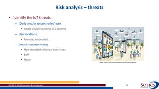
![Case 4: other networked medical devices
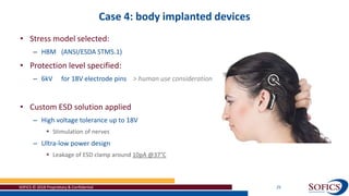
SOFICS © 2018 Proprietary & Confidential 26
• Likelihood and impact differ significantly between applications
– Wearable, external devices have higher likelihood of ESD events
– Life supporting devices (pacemakers) have a bigger impact if things go wrong
Impact
RISK [1] [2] [3] [4] [5]
Likelihood
[A]
[B]
[C]
[D]
[E]](https://image.slidesharecdn.com/2018-09-27soficsatiotworkshop-slideshare-200227111230/85/IoT-workshop-Is-1kV-Also-Enough-for-IoT-ESD-Protection-Do-Current-Test-Methods-and-Models-Apply-26-320.jpg)