This paper analyzes the reliability of MOSFETs that use indium-tin oxide as the gate oxide instead of silicon dioxide. Interface trap charges at the oxide-silicon interface can degrade MOSFET performance by changing the threshold voltage over time. The paper finds that MOSFETs using indium-tin oxide exhibit improved immunity to the effects of interface trap charges compared to those using silicon dioxide. Specifically, indium-tin oxide MOSFETs show enhanced static, linearity, and intermodulation performance metrics when subjected to both positive and negative interface trap charges. Thus, indium-tin oxide has potential to improve MOSFET reliability by reducing sensitivity to interface trap charge effects.


![PN JUNCTION: 2 SEMICONDUCTORS P AND N TYPE ARE
MERGED USING EPITEXIAL TECHNOLOGY, PROVIDING A
DIFFERENT RESPONSE OF VOLTAGE WITH RESPECT TO
CURRENT
A SPACE CHARGE REGION IS FORMED IN A DIODE, WHERE
ONLY IONS AND COVALENT BOND EXISTS RESULTING IN
A BUILT IN POTENTIAL ACROSS THE JUNCTION, (Vbi)
Vbi = Vt ln[NAND/Ni
2]
i.e. Vbi IS STRONGLY DEPENDENT ON TEMPERATURE AND
DOPING CONCENTRAION.
HERE, Vt= KT/q;
K-> BOLTZAMAN CONSTANT
T-> TEMPERATURE
q-> CHARGE
• Vbi CANNOT BE MEASURED DIRECTLY
BY APPPLYING VOLTMETER!](https://image.slidesharecdn.com/presentation1-190211081125/75/MOSFET-ABOUT-FABRICATION-11-2048.jpg)
![DEPLETION WIDTH OF A PN JUNCTION DIODE ALSO
PLAYS AN IMPORTANT ROLE,
DEPLETION WIDTH HIGHLY DEPENDS ON DOPING
CONCENTRATION AND Vbi, ALSO DEPLETION
REGION EXPANDS MORE TO THE SIDE LESS DOPED
IN COMPARISION TO HEAVILY DOPED SIDE.
DIODE CURRENT CAN BE PROVIDED BY THE
FOLLOWING RELATION:
Id= Is[eVd/ῃvt -1] where ῃ is the utility factor.
ῃ =1, recombination current dominates,
ῃ=2, diffusion current dominates.](https://image.slidesharecdn.com/presentation1-190211081125/75/MOSFET-ABOUT-FABRICATION-12-2048.jpg)


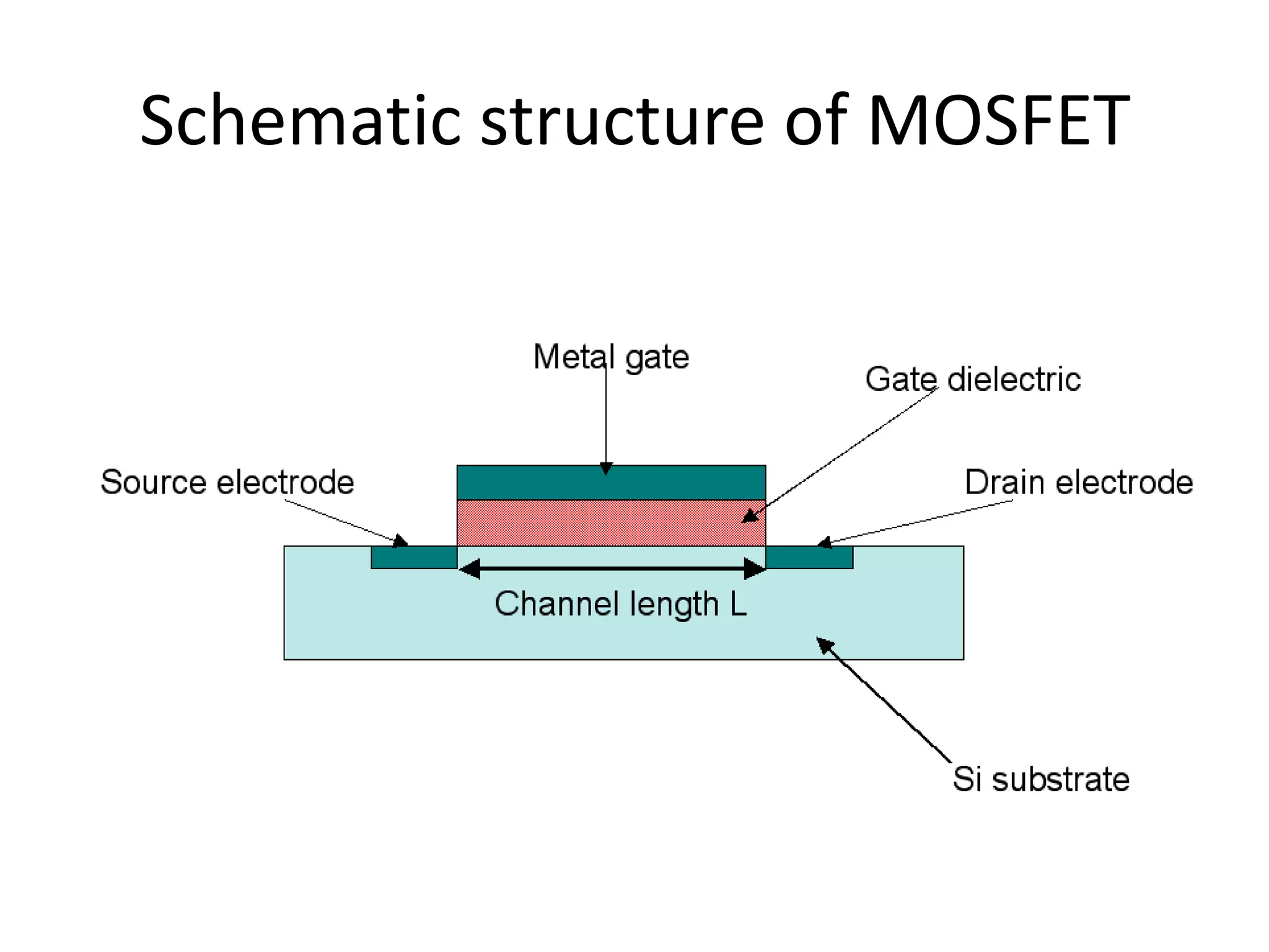
![MOSFET(METAL OXIDE SEMICONDUCTOR FIELD EFECT TRANSISTOR)
• MOSFET IS A 4 TERMINAL
DEVICE[DRAIN,SOURCE,GATE,SUBSTRATE]
• SOURCE AND DRAIN TO SUBSTRATE PN
JUNCTION ARE ALWAYS REVERESE BIASSED,](https://image.slidesharecdn.com/presentation1-190211081125/75/MOSFET-ABOUT-FABRICATION-17-2048.jpg)


![OPERATION OF MOSFET IS DEALT AS:
LINEAR REGION(TRIODE)
SATURATION REGION
BREAKDOWN REGION
IN LINEAR REGION, CURRENT VARIES AS
Id= ʯn Cox (W/L)[VGS-Vth-0.5VDS]VDS
IN SATURATION REGION, CURRENT VARIES AS:
ID= ʯn Cox (W/2L)[VGS-Vth]2
IN BREAKDOWN REGION, HOT CARRIER EFFECT
HAPPENS DUE TO HIGH ELECTRIC FIELD AT DRAIN
END.](https://image.slidesharecdn.com/presentation1-190211081125/75/MOSFET-ABOUT-FABRICATION-20-2048.jpg)