This document summarizes a seminar presentation on photovoltaic cells. The presentation covered:
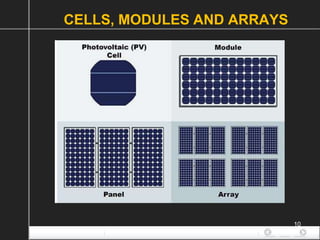
- An introduction to photovoltaics, which are semiconductor devices that convert sunlight to direct current electricity. PV cells are arranged into modules and arrays.
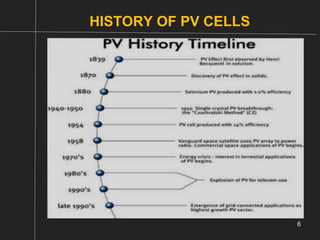
- A brief history of PV cells including early uses to power satellites and navigational aids in the 1950s-1960s and later consumer electronics.
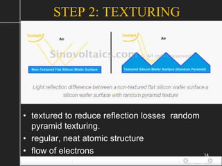
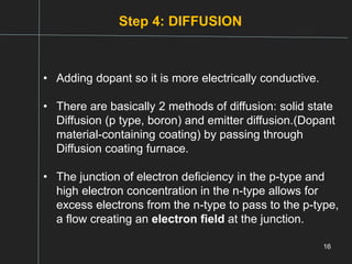
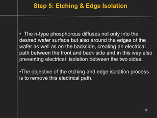
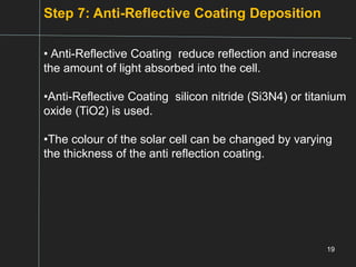
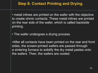
- The 9-step production process for silicon wafer-based PV cells including pre-treatment, texturing, diffusion, anti-reflective coating, contact printing, and final testing and sorting.
CMOS FABRICATION
For less power dissipation requirement CMOS technology is used for implementing transistors. If we require a faster circuit then transistors are implemented over IC using BJT . Fabrication of CMOS transistors as IC’s can be done in three different methods.
The N-well / P-well technology, where n-type diffusion is done over a p-type substrate or p-type diffusion is done over n-type substrate respectively.
P-WELL PROCESS
The fabrication steps of p well process are same as that of an n-well process except that instead of n-well a p-well is implanted . The process steps involved in p-well process are shown in Figure below. The process starts with the n type substrate
The CMOS fabrication process in VLSI.
CMOS (complementary metal-oxide-semiconductor) is the term usually used to describe the small amount of memory on a computer motherboard that stores the BIOS settings.
Cmos fabrication is a part of semiconductor electronics that deals with the designing and fabrication process with NMOS and Cmos and other processes like Twin tub techniques and etc.
Metal oxide semiconductor field emitting transistor is a unipolar high input impedance device usually operated in saturation region for applications like microprocessor, power devices, memories etc.
All about the solar cell for the purpose of usage of solar cells and solar battery bank.if we want to take knowledge for a solar then we should need to know about the conversation of solar energy into electrical energy .
This is not an efficient conversation of energy because the conversation of solar energy in to electrical energy gives the output only 18% output
MONOLITHIC IC PROCESSES A monolithic integrated circuit (IC) is a set of circuitry on a single semiconductor plate or chip rather than built of separate elements as a discrete circuit is.
Overview of advantages and fabrication of solar cells made from silicon nanowires. IT includes few slides of conventional solar cells and benefits of using silicon nanowire.
Solar cell is the device that converts energy of light directly into electrical energy (electricity) by photovoltaic effect In general, a solar cell that includes both solar and non solar sources of light
(such as photons from incandescent bulbs) is termed a photovoltaic cell. Solar cell is also know as photovoltaic cell
Most familiar solar cells are based on the effect
of photovoltaic In this effect, light falling on semiconductor device of the two layer produces a potential difference or photo voltage between the layers The voltage thus produced can drive a current through an external circuit producing useful work
GDG Cloud Southlake #33: Boule & Rebala: Effective AppSec in SDLC using Deplo...James Anderson
Effective Application Security in Software Delivery lifecycle using Deployment Firewall and DBOM
The modern software delivery process (or the CI/CD process) includes many tools, distributed teams, open-source code, and cloud platforms. Constant focus on speed to release software to market, along with the traditional slow and manual security checks has caused gaps in continuous security as an important piece in the software supply chain. Today organizations feel more susceptible to external and internal cyber threats due to the vast attack surface in their applications supply chain and the lack of end-to-end governance and risk management.
The software team must secure its software delivery process to avoid vulnerability and security breaches. This needs to be achieved with existing tool chains and without extensive rework of the delivery processes. This talk will present strategies and techniques for providing visibility into the true risk of the existing vulnerabilities, preventing the introduction of security issues in the software, resolving vulnerabilities in production environments quickly, and capturing the deployment bill of materials (DBOM).
Speakers:
Bob Boule
Robert Boule is a technology enthusiast with PASSION for technology and making things work along with a knack for helping others understand how things work. He comes with around 20 years of solution engineering experience in application security, software continuous delivery, and SaaS platforms. He is known for his dynamic presentations in CI/CD and application security integrated in software delivery lifecycle.
Gopinath Rebala
Gopinath Rebala is the CTO of OpsMx, where he has overall responsibility for the machine learning and data processing architectures for Secure Software Delivery. Gopi also has a strong connection with our customers, leading design and architecture for strategic implementations. Gopi is a frequent speaker and well-known leader in continuous delivery and integrating security into software delivery.
Epistemic Interaction - tuning interfaces to provide information for AI supportAlan Dix
Paper presented at SYNERGY workshop at AVI 2024, Genoa, Italy. 3rd June 2024
https://alandix.com/academic/papers/synergy2024-epistemic/
As machine learning integrates deeper into human-computer interactions, the concept of epistemic interaction emerges, aiming to refine these interactions to enhance system adaptability. This approach encourages minor, intentional adjustments in user behaviour to enrich the data available for system learning. This paper introduces epistemic interaction within the context of human-system communication, illustrating how deliberate interaction design can improve system understanding and adaptation. Through concrete examples, we demonstrate the potential of epistemic interaction to significantly advance human-computer interaction by leveraging intuitive human communication strategies to inform system design and functionality, offering a novel pathway for enriching user-system engagements.
Neuro-symbolic is not enough, we need neuro-*semantic*Frank van Harmelen
Neuro-symbolic (NeSy) AI is on the rise. However, simply machine learning on just any symbolic structure is not sufficient to really harvest the gains of NeSy. These will only be gained when the symbolic structures have an actual semantics. I give an operational definition of semantics as “predictable inference”.
All of this illustrated with link prediction over knowledge graphs, but the argument is general.
Slack (or Teams) Automation for Bonterra Impact Management (fka Social Soluti...Jeffrey Haguewood
Sidekick Solutions uses Bonterra Impact Management (fka Social Solutions Apricot) and automation solutions to integrate data for business workflows.
We believe integration and automation are essential to user experience and the promise of efficient work through technology. Automation is the critical ingredient to realizing that full vision. We develop integration products and services for Bonterra Case Management software to support the deployment of automations for a variety of use cases.
This video focuses on the notifications, alerts, and approval requests using Slack for Bonterra Impact Management. The solutions covered in this webinar can also be deployed for Microsoft Teams.
Interested in deploying notification automations for Bonterra Impact Management? Contact us at sales@sidekicksolutionsllc.com to discuss next steps.
Accelerate your Kubernetes clusters with Varnish CachingThijs Feryn
A presentation about the usage and availability of Varnish on Kubernetes. This talk explores the capabilities of Varnish caching and shows how to use the Varnish Helm chart to deploy it to Kubernetes.
This presentation was delivered at K8SUG Singapore. See https://feryn.eu/presentations/accelerate-your-kubernetes-clusters-with-varnish-caching-k8sug-singapore-28-2024 for more details.
DevOps and Testing slides at DASA ConnectKari Kakkonen
My and Rik Marselis slides at 30.5.2024 DASA Connect conference. We discuss about what is testing, then what is agile testing and finally what is Testing in DevOps. Finally we had lovely workshop with the participants trying to find out different ways to think about quality and testing in different parts of the DevOps infinity loop.
The Art of the Pitch: WordPress Relationships and SalesLaura Byrne
Clients don’t know what they don’t know. What web solutions are right for them? How does WordPress come into the picture? How do you make sure you understand scope and timeline? What do you do if sometime changes?
All these questions and more will be explored as we talk about matching clients’ needs with what your agency offers without pulling teeth or pulling your hair out. Practical tips, and strategies for successful relationship building that leads to closing the deal.
Encryption in Microsoft 365 - ExpertsLive Netherlands 2024Albert Hoitingh
In this session I delve into the encryption technology used in Microsoft 365 and Microsoft Purview. Including the concepts of Customer Key and Double Key Encryption.
Dev Dives: Train smarter, not harder – active learning and UiPath LLMs for do...UiPathCommunity
💥 Speed, accuracy, and scaling – discover the superpowers of GenAI in action with UiPath Document Understanding and Communications Mining™:
See how to accelerate model training and optimize model performance with active learning
Learn about the latest enhancements to out-of-the-box document processing – with little to no training required
Get an exclusive demo of the new family of UiPath LLMs – GenAI models specialized for processing different types of documents and messages
This is a hands-on session specifically designed for automation developers and AI enthusiasts seeking to enhance their knowledge in leveraging the latest intelligent document processing capabilities offered by UiPath.
Speakers:
👨🏫 Andras Palfi, Senior Product Manager, UiPath
👩🏫 Lenka Dulovicova, Product Program Manager, UiPath
UiPath Test Automation using UiPath Test Suite series, part 4DianaGray10
Welcome to UiPath Test Automation using UiPath Test Suite series part 4. In this session, we will cover Test Manager overview along with SAP heatmap.
The UiPath Test Manager overview with SAP heatmap webinar offers a concise yet comprehensive exploration of the role of a Test Manager within SAP environments, coupled with the utilization of heatmaps for effective testing strategies.
Participants will gain insights into the responsibilities, challenges, and best practices associated with test management in SAP projects. Additionally, the webinar delves into the significance of heatmaps as a visual aid for identifying testing priorities, areas of risk, and resource allocation within SAP landscapes. Through this session, attendees can expect to enhance their understanding of test management principles while learning practical approaches to optimize testing processes in SAP environments using heatmap visualization techniques
What will you get from this session?
1. Insights into SAP testing best practices
2. Heatmap utilization for testing
3. Optimization of testing processes
4. Demo
Topics covered:
Execution from the test manager
Orchestrator execution result
Defect reporting
SAP heatmap example with demo
Speaker:
Deepak Rai, Automation Practice Lead, Boundaryless Group and UiPath MVP
3. INTRODUCTION
3
Photovoltaics (PV) or solar cells are semiconductor
devices that convert sunlight into direct current (DC)
electricity.
Groups of PV cells are electrically configured into
modules and arrays, which can be used to charge
batteries, operate motors, and to power any number of
electrical loads.
With the appropriate power conversion equipment, PV
systems can produce alternating current (AC)
compatible with any conventional appliances, and can
operate in parallel with, and interconnected to, the
utility grid
11. TYPES OF PV CELLS
11
Made by using
crystalline solid solar
cells, developed from
micro electronics
technology industry
Mono crystalline PV
cells
Multi crystalline PV
cells
Made by depositing one
or more thin photo
voltaic material on
substrate
Amorphous silicon PV
cells
Poly crystalline PV cells
13. • Raw silicon wafer- pre-check - geometric
shape and thickness conformity and damages such as cracks,
breakages, scratches or other anomalities.
• Then the wafers are split and cleaned with industrial soaps to
remove any metal residues, liquids or other production
remains from the surface that would otherwise impact the
efficiency of that wafer.
13
Step 1: Pre-check and Pretreatment
14. STEP 2: TEXTURING
• textured to reduce reflection losses random
pyramid texturing.
• regular, neat atomic structure
• flow of electrons 14
15. Step 3: Acid Cleaning
15
• acidic rinsing means remove the post texturing
particles which remains their.
• hydrogen flouride (HF) vapor
• hydrogen chloride (HCl)
16. Step 4: DIFFUSION
16
• Adding dopant so it is more electrically conductive.
• There are basically 2 methods of diffusion: solid state
Diffusion (p type, boron) and emitter diffusion.(Dopant
material-containing coating) by passing through
Diffusion coating furnace.
• The junction of electron deficiency in the p-type and
high electron concentration in the n-type allows for
excess electrons from the n-type to pass to the p-type,
a flow creating an electron field at the junction.
17. Step 5: Etching & Edge Isolation
17
• The n-type phosphorous diffuses not only into the
desired wafer surface but also around the edges of the
wafer as well as on the backside, creating an electrical
path between the front and back side and in this way also
preventing electrical isolation between the two sides.
•The objective of the etching and edge isolation process
is to remove this electrical path.
18. Step 6: Post-Etching Washing
18
• After the etching, particle residues potential remain on
the wafer and the wafer edges. Therefore the wafers
need to undergo a second washing to remove remains of
the previous etching process.
•After this second washing, the wafers can further be
processed for the deposition of anti-reflective (AR)
coating.
19. Step 7: Anti-Reflective Coating Deposition
19
• Anti-Reflective Coating reduce reflection and increase
the amount of light absorbed into the cell.
•Anti-Reflective Coating silicon nitride (Si3N4) or titanium
oxide (TiO2) is used.
•The colour of the solar cell can be changed by varying
the thickness of the anti reflection coating.
20. Step 8: Contact Printing and Drying
20
• metal inlines are printed on the wafer with the objective
to create ohmic contacts. These metal inlines are printed
on the rear side of the wafer, which is called backside
printing.
• The wafer undergoes a drying process.
•After all contacts have been printed on the rear and front
sides, the screen-printed wafers are passed through
a sintering furnace to solidify the dry metal pastes onto
the wafers. Then, the wafers are cooled.
21. Step 9: Testing and Cell Sorting
21
In this final process, the now ready-to-assemble solar
cells are tested under simulated sunlight conditions and
then classified and sorted according to their efficiencies.
This is handled by a solar cell testing device that
automatically tests and sorts the cells.
S-EMS produces a stirring force that pushes the liquid steel horizontally along the cast product width and generates a butterfly type flow pattern in the liquid steel. When S-EMS can be placed behind the support rollers (Fig. 2 ) then it is not dependent on a minimum support roller diameter and hence in this case can be optimally placed along the strand from the metallurgical point of view. S – EMS when built into the support rollers requires a minimum roller diameter to include the iron core and windings. In this case the stirrer is placed at a distance from the meniscus and hence is less effective. S -EMS operates at low frequency to ensure good penetration of the stirrer force through the strand. As a result the liquid steel has transverse stirring as shown in Fig 2. S –EMS is usually used in combination with M – EMS. S – EMS can be of either linear or rotary type stirrer. Most common is the linear stirrer, which is easy to install and protect against heat radiation and possible breakouts. S-EMS promotes the formation of equiaxed structure. It promotes grain refinement in the cast product and reduces the shrinkage cavity, centre segregation and internal cracks. It also removes superheat effectively.