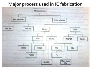
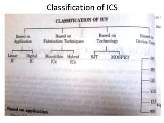
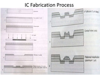
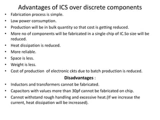
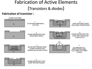
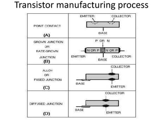
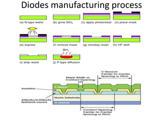
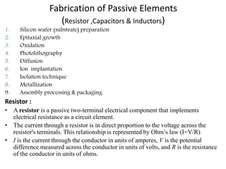
Very Large Scale Integration is the technology used now a day everywhere. Diploma as well as degree students can refer this
(For Downloads, send me mail
agarwal.avanish@yahoo.com)
Very-large-scale integration (VLSI) is the process of creating an integrated circuit (IC) by combining thousands of transistors into a single chip. VLSI began in the 1970s when complex semiconductor and communication technologies were being developed. The microprocessor is a VLSI device. Before the introduction of VLSI technology most ICs had a limited set of functions they could perform. An electronic circuit might consist of a CPU, ROM, RAM and other glue logic. VLSI lets IC designers add all of these into one chip.
The History of the transistor dates to the mid-1920s when several inventors attempted devices that were intended to control current in solid-state diodes and convert them into triodes. Success came after World War II, when the use of silicon and germanium crystals as radar detectors led to improvements in fabrication and theory. Scientists who had worked on radar returned to solid-state device development. With the invention of transistors at Bell Labs in 1947, the field of electronics shifted from vacuum tubes to solid-state devices.
With the small transistor at their hands, electrical engineers of the 1950s saw the possibilities of constructing far more advanced circuits. However, as the complexity of circuits grew, problems arose.
One problem was the size of the circuit. A complex circuit like a computer was dependent on speed. If the components were large, the wires interconnecting them must be long. The electric signals took time to go through the circuit, thus slowing the computer.
The Invention of the integrated circuit by Jack Kilby and Robert Noyce solved this problem by making all the components and the chip out of the same block (monolith) of semiconductor material. The circuits could be made smaller, and the manufacturing process could be automated. This led to the idea of integrating all components on a single silicon wafer, which led to small-scale integration (SSI) in the early 1960s, medium-scale integration (MSI) in the late 1960s, and then large-scale integration (LSI) as well as VLSI in the 1970s and 1980s, with tens of thousands of transistors on a single chip (later hundreds of thousands, then millions, and now billions (109)).
These presentation was given to Electronics and Communication Students, Sem6, CENTRAL INSTITUTE OF TECHNOLOGY(CIT) KOKRAJHAR. This presentation includes general overview of VLSI industry and career guidance for VLSI industry. The program was initiated by Dr. Agile Mathew, Assistant Professor at CIT.
IOSR journal of VLSI and Signal Processing (IOSRJVSP) is an open access journal that publishes articles which contribute new results in all areas of VLSI Design & Signal Processing. The goal of this journal is to bring together researchers and practitioners from academia and industry to focus on advanced VLSI Design & Signal Processing concepts and establishing new collaborations in these areas.
Introduction to semiconductor lasers, and its working. construction of semiconductor laser, Ga As laser, and construction, achievement of population inversion, pumping.
EDC Unit-5 Introduction to Integrated Circuits (ICs) | RGPV De BunkersRGPV De Bunkers
The PDF document "Fundamentals of Integrated Circuits" provides a comprehensive overview of the subject "Electronic Devices & Circuits" for Semester 3 in the Bachelor of Engineering program in Computer Science at Rajiv Gandhi Proudyogiki Vishwavidyalaya Bhopal. Designed to cater to both students and electronics enthusiasts, this document delves into the core concepts of Integrated Circuits (ICs), their fabrication process, and general IC technology.
The first unit, "Introduction to Integrated Circuits (ICs)," sets the foundation by introducing the revolutionary technology of ICs. It explores the integration of multiple active and passive components onto a single semiconductor chip. Emphasizing the advantages of ICs, the document highlights their role in miniaturizing electronic devices, cost-effectiveness in mass production, enhanced reliability, power efficiency, and high-performance capabilities. However, it also discusses the limitations, such as complex design processes and difficulty in repair and maintenance.
The second unit, "Classification of Integrated Circuits," categorizes ICs based on complexity, application, and technology. From Small-Scale Integration (SSI) to Very-Large-Scale Integration (VLSI), it covers the wide spectrum of IC complexities. The distinction between analog ICs, digital ICs, and mixed-signal ICs is explored in terms of their distinct applications. Moreover, the choice between bipolar ICs and CMOS ICs is elaborated upon, explaining the trade-offs between performance and power consumption.
In the third unit, "Production Process of Monolithic ICs," the document delves into the intricate fabrication steps required to create monolithic ICs. From selecting the semiconductor wafer material to heat treatment and testing, each stage of the process is explained in detail. The photolithographic process, an essential part of IC fabrication, is thoroughly covered, encompassing photoresist coating, mask alignment, exposure, developing, and subsequent etching or ion implantation.
The unit further explores unipolar ICs, focusing on N-channel and P-channel Metal-Oxide-Semiconductor Field-Effect Transistors (MOSFETs). It explains how these transistors are used as essential components in digital and analog integrated circuits.
The final topic, "IC Symbols," introduces standardized graphical representations commonly used in circuit diagrams to depict various types of integrated circuits and their functions. Understanding these symbols is fundamental for interpreting and designing electronic circuits accurately.
This comprehensive PDF document serves as an invaluable resource for students and electronics enthusiasts seeking to grasp the fundamentals of Integrated Circuits and Electronic Devices & Circuits. With a detailed explanation of each topic and sub-topic, along with real-world applications, it equips readers with the knowledge required to pursue advanced studies and excel in the dynamic field of electronics.
In this presentation of mine, a basic Design approach of VLSI has been explained. The ppt explains the market level of VLSI and also the fabrication process and also its various applications. An integration of various switches, gates, etc on Ic's has also been showcased in the same.
Student information management system project report ii.pdfKamal Acharya
Our project explains about the student management. This project mainly explains the various actions related to student details. This project shows some ease in adding, editing and deleting the student details. It also provides a less time consuming process for viewing, adding, editing and deleting the marks of the students.
TECHNICAL TRAINING MANUAL GENERAL FAMILIARIZATION COURSEDuvanRamosGarzon1
AIRCRAFT GENERAL
The Single Aisle is the most advanced family aircraft in service today, with fly-by-wire flight controls.
The A318, A319, A320 and A321 are twin-engine subsonic medium range aircraft.
The family offers a choice of engines
About
Indigenized remote control interface card suitable for MAFI system CCR equipment. Compatible for IDM8000 CCR. Backplane mounted serial and TCP/Ethernet communication module for CCR remote access. IDM 8000 CCR remote control on serial and TCP protocol.
• Remote control: Parallel or serial interface.
• Compatible with MAFI CCR system.
• Compatible with IDM8000 CCR.
• Compatible with Backplane mount serial communication.
• Compatible with commercial and Defence aviation CCR system.
• Remote control system for accessing CCR and allied system over serial or TCP.
• Indigenized local Support/presence in India.
• Easy in configuration using DIP switches.
Technical Specifications
Indigenized remote control interface card suitable for MAFI system CCR equipment. Compatible for IDM8000 CCR. Backplane mounted serial and TCP/Ethernet communication module for CCR remote access. IDM 8000 CCR remote control on serial and TCP protocol.
Key Features
Indigenized remote control interface card suitable for MAFI system CCR equipment. Compatible for IDM8000 CCR. Backplane mounted serial and TCP/Ethernet communication module for CCR remote access. IDM 8000 CCR remote control on serial and TCP protocol.
• Remote control: Parallel or serial interface
• Compatible with MAFI CCR system
• Copatiable with IDM8000 CCR
• Compatible with Backplane mount serial communication.
• Compatible with commercial and Defence aviation CCR system.
• Remote control system for accessing CCR and allied system over serial or TCP.
• Indigenized local Support/presence in India.
Application
• Remote control: Parallel or serial interface.
• Compatible with MAFI CCR system.
• Compatible with IDM8000 CCR.
• Compatible with Backplane mount serial communication.
• Compatible with commercial and Defence aviation CCR system.
• Remote control system for accessing CCR and allied system over serial or TCP.
• Indigenized local Support/presence in India.
• Easy in configuration using DIP switches.
CFD Simulation of By-pass Flow in a HRSG module by R&R Consult.pptxR&R Consult
CFD analysis is incredibly effective at solving mysteries and improving the performance of complex systems!
Here's a great example: At a large natural gas-fired power plant, where they use waste heat to generate steam and energy, they were puzzled that their boiler wasn't producing as much steam as expected.
R&R and Tetra Engineering Group Inc. were asked to solve the issue with reduced steam production.
An inspection had shown that a significant amount of hot flue gas was bypassing the boiler tubes, where the heat was supposed to be transferred.
R&R Consult conducted a CFD analysis, which revealed that 6.3% of the flue gas was bypassing the boiler tubes without transferring heat. The analysis also showed that the flue gas was instead being directed along the sides of the boiler and between the modules that were supposed to capture the heat. This was the cause of the reduced performance.
Based on our results, Tetra Engineering installed covering plates to reduce the bypass flow. This improved the boiler's performance and increased electricity production.
It is always satisfying when we can help solve complex challenges like this. Do your systems also need a check-up or optimization? Give us a call!
Work done in cooperation with James Malloy and David Moelling from Tetra Engineering.
More examples of our work https://www.r-r-consult.dk/en/cases-en/
Welcome to WIPAC Monthly the magazine brought to you by the LinkedIn Group Water Industry Process Automation & Control.
In this month's edition, along with this month's industry news to celebrate the 13 years since the group was created we have articles including
A case study of the used of Advanced Process Control at the Wastewater Treatment works at Lleida in Spain
A look back on an article on smart wastewater networks in order to see how the industry has measured up in the interim around the adoption of Digital Transformation in the Water Industry.
Automobile Management System Project Report.pdfKamal Acharya
The proposed project is developed to manage the automobile in the automobile dealer company. The main module in this project is login, automobile management, customer management, sales, complaints and reports. The first module is the login. The automobile showroom owner should login to the project for usage. The username and password are verified and if it is correct, next form opens. If the username and password are not correct, it shows the error message.
When a customer search for a automobile, if the automobile is available, they will be taken to a page that shows the details of the automobile including automobile name, automobile ID, quantity, price etc. “Automobile Management System” is useful for maintaining automobiles, customers effectively and hence helps for establishing good relation between customer and automobile organization. It contains various customized modules for effectively maintaining automobiles and stock information accurately and safely.
When the automobile is sold to the customer, stock will be reduced automatically. When a new purchase is made, stock will be increased automatically. While selecting automobiles for sale, the proposed software will automatically check for total number of available stock of that particular item, if the total stock of that particular item is less than 5, software will notify the user to purchase the particular item.
Also when the user tries to sale items which are not in stock, the system will prompt the user that the stock is not enough. Customers of this system can search for a automobile; can purchase a automobile easily by selecting fast. On the other hand the stock of automobiles can be maintained perfectly by the automobile shop manager overcoming the drawbacks of existing system.
Sachpazis:Terzaghi Bearing Capacity Estimation in simple terms with Calculati...Dr.Costas Sachpazis
Terzaghi's soil bearing capacity theory, developed by Karl Terzaghi, is a fundamental principle in geotechnical engineering used to determine the bearing capacity of shallow foundations. This theory provides a method to calculate the ultimate bearing capacity of soil, which is the maximum load per unit area that the soil can support without undergoing shear failure. The Calculation HTML Code included.
Democratizing Fuzzing at Scale by Abhishek Aryaabh.arya
Presented at NUS: Fuzzing and Software Security Summer School 2024
This keynote talks about the democratization of fuzzing at scale, highlighting the collaboration between open source communities, academia, and industry to advance the field of fuzzing. It delves into the history of fuzzing, the development of scalable fuzzing platforms, and the empowerment of community-driven research. The talk will further discuss recent advancements leveraging AI/ML and offer insights into the future evolution of the fuzzing landscape.
2. Microelectronics & Integrated Circuits
Microelectronics-
• It is defined as that area of technology associated with and applied to the
realization of electronic systems made of extremely small electronic parts
or elements.
• The term microelectronics is normally associated with integrated circuits
(IC).
• As the name suggest ue related to the study and
manufacturing(fabrication) of very small electronic design & components.
These device are made of semiconductor materials.Microelectronics
include active(transistors & diodes) and passive(R,L,C) components.
Integrated Ckt-
• It is an electronic assembly built in such a way that all the components in
the ckt are fabricated on a single container called the chip.(For
interconnection metallization is used)
• Silicon is generally used for IC fabrication.
• Temperature range Si-150◦C,Ge-100◦C,low leakage current,abundance.
5. a) Based on application :
• Linear ICS : These are discrete circuits which need external components like
resistor and capacitor for satisfactory performance apart from the input.They
work on analog signals rather than digital signals.eg-op-
amp,ADC,DAC,Timer(555).
• Digital ICS : They require only digital input and not any other component for
operation.eg-all ics likelogic gates,adders,comparaters etc.
b) Based on fabrication techniques :
• Monolithic ICS : All the active and passive components of a circuit can be
fabricated on a single piece of slicon.(Metallization is used for interconnection).
In this ic fabrication process is complex as this is used for fabrication of large
value of components.It involves many different fabrication techniques such as
oxidation,ion implantation,deposition of new material etc.eg-uchip,computer
chip,silicon chip,ic.
• Hybrid ICS : Separate components parts are attached to a ceramic substrate and
interconnected by means of either metallization pattern or wire bonds.
The only difference between monolithic & hybrid is their manufacturing
(fabrication) and construction.
6. Based on technology :
a) BJT – BIPOLAR
MOSFET – NMOS (N-Channel MOS)
PMOS (P-Channel MOS)
CMOS (Complimentary MOS)
BICMOS
Based on device count :
Nomenclature Active Device Typical function
SSI 1-100 gates,opamps
MSI 100-1000 Registers,filters etc
LSI 1000-100000 Up,a/d
VLSI 10*5 to 10*6 Memories,computers,signal processors
ULSI 10*6 Ultra large scale integration(used in japan)
7. IC Production Process
For fabrication of any ICS i.e. monolithic or hybrid various process are :
a) NMOS Process
b) CMOS Process
c) Bipolar Process
Processing Steps :
1) Crystal preparation : The substrate of ICS is generaliy a single crystal of silicon of
high purity which is lightly doped with impurities of n-type for a p-type
material and vice versa.
2) Masking(pattern generation) : Masks are produced by phtolithographic process.
In this process photoresist is applied to entire surface of wafer.Its physical
characterstics can be changed by exposure to light.In some methods laser beam
or E-beam may be used for developing the mask on the surface of wafer.2 types
of photoresist are there negative and positive photoresist.
3) Deposition : Films of various materials must be applied to the wafer during
processing,eg insulators,resistive films,conductive films,n and p type
semiconductor materials,dopants.For deposition we use CVD(chemical vapour
deposition) or PVD(physical vapour deposition).
4) Etching : Now by etching we remove the unwanted material from the substrate
by using photoresist and masks with the help of UV light.
8. 1) Diffusion : It refers to controlled forced migration of impurities into the
substrate of adjacent material.Diffusion will occur between any silicon that has
different densities of impurity with impurity tending to diffuse from high conc.
area to low conc. area.Deposition and implantattion are different diffusion
techniques.
2) Oxidation : For producing SiO2 layer oxidation process is carried out so that
oxide is grown on the surface of substrate.This serves as a very good
insulator.Oxidation process consumes silicon.2 common approaches are
oxidation and dry oxidation.
3) Epitaxy (carried out only in bipolar process) : This involves growing a single
crystal film on the silicon surface.This is done by CVD.
4) Conductors and resistors : For interconnection of components on an IC
aluminium or other metals are generally used.
5) Packaging & testing : After processing,the ICS are tested and packaged.
10. Advantages of ICS over discrete components
• Fabrication process is simple.
• Low power consumption.
• Production will be in bulk quantity so that cost is getting reduced.
• More no of components will be fabricated in a single chip of IC.So size will be
reduced.
• Heat dissipation is reduced.
• More reliable.
• Space is less.
• Weight is less.
• Cost of production of electronic ckts due to batch production is reduced.
Disadvantages :
• Inductors and transformers cannot be fabricated.
• Capacitors with values more than 30pf cannot be fabricated on chip.
• Cannot withstand rough handling and excessive heat.(If we increase the
current, heat dissipation will be increased).
11. Bipolar and MOS Technology
1) Bipolar device : The basic active device used is BJT. The speed is very high with
bipolar process.
2) MOS Device :
• NMOS : primarily used in many applications, as mobility of p-type material is
poorer than n-type.Also it has excellent density and good performance.
• PMOS : It is dual of NMOS. The basic active device is the p-channel MOSFET.
• CMOS : Complementary MOS : It comprises both PMOS & NMOS.CMOS offers
improvement in power dissipation and performance when compared with
NMOS.
• BiCMOS : It is a combination of bipolar CMOS transistors Therefore in BiCMOS
technology we can have the advantages of both bipolar & CMOS technology.This
seems to be effective in speeding up VLSI ckts.
1) Bipolar device : The basic active device are NPN,PNP and BJT,UJT.
• Unipolar junction transistor(UJT) : Current conduction is due to only one type of
charge carriers i.e.majority charge carriers.
• Bipolar junction transistors : Current conduction is due to both the type of charge
carriers i.e. holes & electrons are majority and minority charge carriers.
12. NPN & PNP Transistors
Transistor can raise the strength of a weak signal hence it is used for amplification.It
consist of 2 PN junctionwith junctions formed by sandwiching either p-type or n-
type semiconductor layers a pair of opposite types.
13. MOSFET
MOSFET,gate is isolated from channel so –ve and +ve VGS can be applied.In
MOSFET gate is insulated from its conducting channel by an ultra thin metal oxide
insulating film (SiO2).Hence it is called as IGFET.
a) Depletion Enhancement MOSFET
b) Enhancement only MOSFET
Enhancement only MOSFET : It operates only in enhancement mode and has
no deplition mode.It has no channel between drain and source.
14. Working
• When Vgs=0 or Vgs<Vt then Id=0 i.e. drain current is 0.
• When Vds is applied or Vgs>Vt then Id flows i.e. drain current starts flowinf and
it is equal to
Id=K(Vgs-Vt)*2
K=design or conductivity parameter.
Transfer characterstics :
18. Fabrication of Passive Elements
(Resistor ,Capacitors & Inductors)
1. Silicon wafer (substrate) preparation
2. Epitaxial growth
3. Oxidation
4. Photolithography
5. Diffusion
6. Ion implantation
7. Isolation technique
8. Metallization
9. Assembly processing & packaging
Resistor :
• A resistor is a passive two-terminal electrical component that implements
electrical resistance as a circuit element.
• The current through a resistor is in direct proportion to the voltage across the
resistor's terminals. This relationship is represented by Ohm’s law (I=V/R)
• I is the current through the conductor in units of amperes, V is the potential
difference measured across the conductor in units of volts, and R is the resistance
of the conductor in units of ohms.
20. Capacitors (Farads)
• Capacitor is a basic storage device to store electrical charges and release it as it is
required by the circuit. In a simple form it is made of two conductive plates
(Electrodes) and an insulating media (Dielectrics) which separate the electrodes.
• The charges (Q) on the capacitor plates depend on the voltage (V)and the
capacitance value (C) and is as follows:
Q=C.V
n-Si
SiO
2
n-Si
GROW 4000 A OXIDE ON N-TYPE SILICON
MATERIAL
PATTERN AND ETCH OXIDE<THEN ION
IMPLANT 50 KeV BORON TO FROM P+
REGION
Thin SiO2
Al
n-Si n-Si
GROW THIN OXIDE (2000 A)
PATTERN AND ETCH OXIDE TO FROM
CONTACT
DEPOSIT 5000A ALUMINUM
PATTERN AND ETCH ALUMINUM
21. Inductors (henry)
• An inductor (also choke, coil or reactor) is a passive two terminal electrical
component that stores energy in its magnetic field. For comparison,
a capacitor stores energy in an electric field, and a resistor does not store
energy but rather dissipates energy as heat.
• Any conductor has inductance. An inductor is typically made of a wire or other
conductor wound into a coil, to increase the magnetic field.
22.
23. Uncertainties in IC Fabrication
• The precision of transistors and passive components fabricated using IC
technology is surprisingly, poor.
Sources of variations:
• Ion impant dose varies from point to point over the wafer and from wafer to
wafer.
• Thicknesses of layers after annealing vary due to temperature variations across
the wafer.
• Widths of regions vary systematically due to imperfect wafer flatness (leading
to focus problems) and randomly due to raggedness in the photoresist edges
after development.
24. PACKAGING TECHNIQUES
Once the IC has been produced, it requires a housing that will protect it from
damage. This damage could result from moisture, dirt, heat, radiation, or other
sources. The housing protects the device and aids in its handling and connection into
the system in which the IC is used.The three most common types of packages are
TRANSISTOR-OUTLINE (TO) PACKAGE, FLAT PACK, DUAL INLINE PACKAGE (DIP).
DUAL INLINE PACKAGE : The dual inline package (DIP) was designed primarily to
overcome the difficulties associated with handling and inserting packages into
mounting boards. DIPs are easily inserted by hand or machine and require no
spreaders, spacers, insulators, or lead-forming tools. Standard hand tools and
soldering irons can be used to field-service the devices. Plastic DIPs are finding wide
use in commercial applications, and a number of military systems are incorporating
ceramic DIPS.
25. Transitor-Outline Package :
The transistor-outline (TO) package was developed from early experience with
transistors. It was a reliable package that only required increasing the number of
leads to make it useful for ICs. Leads normally number between 2 and 12, with 10
being the most common for IC applications. Once the IC has been attached to the
header, bonding wires are used to attach the IC to the leads. The cover provides the
necessary protection for the device. You can easily see that the handling of an IC
without packaging would be difficult for a technician.
26. Flat pack
Many types of IC flat packs are being produced in various sizes and materials.
These packages are available in square, rectangular, oval, and circular
configurations with 10 to 60 external leads. They may be made of metal,
ceramic, epoxy, glass, or combinations of those materials.
27. SSI,MSI,LSI & VLSI
• SSI : Small Scale Integration
• MSI : Medium Scale Integration
• LSI : Large Scale Integration
• VLSI : Very Large Scale Integration
28. VLSI
Very Large Scale Integration
• design/manufacturing of extremely small, complex circuitry using modified
semiconductor material
• integrated circuit (IC) may contain millions of transistors, each a few mm in
size
• applications wide ranging: most electronic logic devices.
Origins of VLSI
• Much development motivated by WWII need for improved electronics,
especially for radar
• 1940 - Russell Ohl (Bell Laboratories) - first pn junction
• 1948 - Shockley, Bardeen, Brattain (Bell Laboratories) - first transistor
• 1956 Nobel Physics Prize
• Late 1950s - purification of Si advances to acceptable levels for use in electronics
• 1958 - Seymour Cray (Control Data Corporation) - first transistorized computer -
CDC 1604.
• 1959 - Jack St. Claire Kilby (Texas Instruments) - first integrated circuit - 10
components on 9 mm2
29. • 1959 - Robert Norton Noyce (founder, Fairchild Semiconductor) - improved
integrated circuit.
• 1968 - Noyce, Gordon E. Moore found Intel.
• 1971 - Ted Hoff (Intel) - first microprocessor (4004) - 2300 transistors on 9 mm2
• Since then - continued improvement in technology has allowed for increased
performance as predicted by Moore’s Law.
Three Dimensional VLSI
• The fabrication of a single integrated circuit whose functional parts (transistors,
etc) extend in three dimensions.
• The vertical orientation of several bare integrated circuits in a single package.
Advantages of VLSI :
• Low power dissipation.
• Area consumption is less.
• Power consumption is less.
• High speed of operation.