Downloaded 134 times


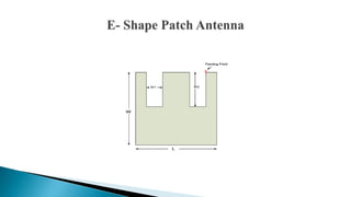
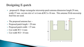
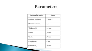
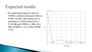
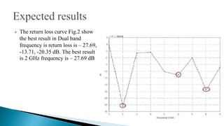


The document describes the design and simulation of an E-shaped microstrip patch antenna. Key details include: 1) The antenna has a proposed patch length of 29mm and width of 37mm, with cuts of 6mm and 18mm. 2) The antenna was simulated in IE3D from 1-9GHz with a dielectric constant of 4.3, thickness of 1.5mm, and loss tangent of 0.019. 3) The simulation results showed dual-band behavior with best return losses of -27.69dB at 2GHz, -13.71dB at 6GHz, and -20.35dB at 8GHz. VSWR was lowest at 2GHz at 1.