This document is the preface to the second edition of the book "Microstrip and Printed Antenna Design" by Randy Bancroft. It provides an overview of the additions and improvements made for the second edition, including new analysis methods for circular polarization bandwidth, expanded sections on omnidirectional and PIFA antennas, and the addition of impedance matching techniques. The preface expresses the goal of the book as providing practical and manufacturable antenna designs while also offering references for more complex designs. It is intended as a handbook for microstrip antenna designers.


![Chapter 1
Microstrip Antennas
1.1 The Origin of Microstrip Radiators
The use of coaxial cable and parallel two wire (or “twin lead”) as a transmis-
sion line can be traced to at least the 19th century. The realization of radio
frequency (RF) and microwave components using these transmission lines
required considerable mechanical effort in their construction. The advent of
printed circuit board techniques in the mid-20th century led to the realization
that printed circuit versions of these transmission lines could be developed
which would allow for much simpler mass production of microwave compo-
nents. The printed circuit analog of a coaxial cable became known as stripline.
With a groundplane image providing a virtual second conductor, the printed
circuit analog of two wire (“parallel plate”) transmission line became known
as microstrip. For those not familiar with the details of this transmission line,
they can be found in Appendix B at the end of this book.
Microstrip geometries which radiate electromagnetic waves were originally
contemplated in the 1950s. The realization of radiators that are compatible with
microstrip transmission line is nearly contemporary, with its introduction in
1952 by Grieg and Englemann.[1]
The earliest known realization of a microstrip-
like antenna integrated with microstrip transmission line was developed in
1953 by Deschamps[2,3]
(Figure 1-1). By 1955, Gutton and Baissinot patented a
microstrip antenna design.[4]
Early microstrip lines and radiators were specialized devices developed in
laboratories. No commercially available printed circuit boards with controlled
dielectric constants were developed during this period. The investigation of
microstrip resonators that were also efficient radiators languished. The theo-
retical basis of microstrip transmission lines continued to be the object of
academic inquiry.[5]
Stripline received more interest as a planar transmission
1](https://image.slidesharecdn.com/1891121731microstrip-151111163821-lva1-app6892/85/1891121731-microstrip-9-320.jpg)
![2 Microstrip Antennas
line at the time because it supports a transverse electromagnetic (TEM) wave
and allowed for easier analysis, design, and development of planar microwave
structures. Stripline was also seen as an adaptation of coaxial cable and
microstrip as an adaptation of two wire transmission line. R. M. Barrett opined
in 1955 that the “merits of these two systems [stripline and microstrip] are
essentially the merits of their respective antecedents [coaxial cable and two
wire].”[6]
These viewpoints may have been some of the reasons microstrip did
not achieve immediate popularity in the 1950s. The development of microstrip
transmission line analysis and design methods continued in the mid to late
1960s with work by Wheeler[7]
and Purcel et al.[8,9]
In 1969 Denlinger noted rectangular and circular microstrip resonators
could efficiently radiate.[10]
Previous researchers had realized that in some
cases, 50% of the power in a microstrip resonator would escape as radiation.
Denlinger described the radiation mechanism of a rectangular microstrip reso-
nator as arising from the discontinuities at each end of a truncated microstrip
transmission line. The two discontinuities are separated by a multiple of a half
wavelength and could be treated separately and combined to describe the
complete radiator. It was noted that the percentage of radiated power to the
Figure 1-1 Original conformal array designed by Deshamps [2] in 1953 fed with
microstrip transmission line.](https://image.slidesharecdn.com/1891121731microstrip-151111163821-lva1-app6892/85/1891121731-microstrip-10-320.jpg)
![Microstrip Antennas 3
total input power increased as the substrate thickness of the microstrip radia-
tor increased. These correct observations are discussed in greater detail in
Chapter 2. Denlinger’s results only explored increasing the substrate thickness
until approximately 70% of the input power was radiated into space. Denlinger
also investigated radiation from a resonant circular microstrip disc. He observed
that at least 75% of the power was radiated by one circular resonator under
study. In late 1969, Watkins described the fields and currents of the resonant
modes of circular microstrip structures.[11]
The microstrip antenna concept finally began to receive closer examination
in the early 1970s when aerospace applications, such as spacecraft and mis-
siles, produced the impetus for researchers to investigate the utility of con-
formal antenna designs. In 1972 Howell articulated the basic rectangular
microstrip radiator fed with microstrip transmission line at a radiating edge.[12]
The microstrip resonator with considerable radiation loss was now described
as a microstrip antenna. A number of antenna designers received the design
with considerable caution. It was difficult to believe a resonator of this type
could radiate with greater than 90% efficiency. The narrow bandwidth of the
antenna seemed to severely limit the number of possible applications for which
the antenna could prove useful. By the late 1970s, many of these objections
had not proven to derail the use of microstrip antennas in numerous aerospace
applications. By 1981, microstrip antennas had become so ubiquitous and
studied that they were the subject of a special issue of the IEEE Transactions
on Antennas and Propagation.[13]
Today a farrago of designs have been developed, which can be bewildering
to designers who are new to the subject. This book attempts to explain basic
concepts and present useful designs. It will also direct the reader who wishes
to research other microstrip antenna designs, which are not presented in this
work, to pertinent literature.
The geometry which is defined as a microstrip antenna is presented in
Figure 1-2. A conductive patch exists along the plane of the upper surface of
a dielectric slab. This area of conductor, which forms the radiating element, is
generally rectangular or circular, but may be of any shape. The dielectric
substrate has groundplane on its bottom surface.](https://image.slidesharecdn.com/1891121731microstrip-151111163821-lva1-app6892/85/1891121731-microstrip-11-320.jpg)
![4 Microstrip Antennas
1.2 Microstrip Antenna Analysis Methods
It was known that the resonant length of a rectangular microstrip antenna is
approximately one-half wavelength with the effective dielectric constant of the
substrate taken into account. Following the introduction of the microstrip
antenna, analysis methods were desired to determine the approximate
resonant resistance of a basic rectangular microstrip radiator. The earliest
useful model introduced to provide approximate values of resistance at
the edge of a microstrip antenna is known as the transmission line model,
introduced by Munson.[14]
The transmission line model provides insight into
the simplest microstrip antenna design, but is not complete enough to be
useful when more than one resonant mode is present. In the late 1970s
Lo et al. developed a model of the rectangular microstrip antenna as a
lossy resonant cavity.[15]
Microstrip antennas, despite their simple geometry,
proved to be very challenging to analyze using exact methods. In the 1980s,
the method of moments (MoM) became the first numerical analysis method
that was computationally efficient enough so that contemporary computers
Figure 1-2 Geometry of a microstrip antenna.](https://image.slidesharecdn.com/1891121731microstrip-151111163821-lva1-app6892/85/1891121731-microstrip-12-320.jpg)
![Microstrip Antennas 5
could provide enough memory and CPU speed to practically analyze microstrip
antennas.[16–19]
Improvements in computational power and memory size of personal com-
puters during the 1990s made numerical methods such as the finite difference
time domain (FDTD) method and finite element method (FEM), which require
much more memory than MoM solutions, workable for everyday use by design-
ers. This book will generally use FDTD as a full-wave analysis method as well
as Ansoft HFSS.[20,21]
1.3 Microstrip Antenna Advantages and Disadvantages
The main advantages of microstrip antennas are:
• Low-cost fabrication.
• Can easily conform to a curved surface of a vehicle or product.
• Resistant to shock and vibration (most failures are at the feed probe solder
joint).
• Many designs readily produce linear or circular polarization.
• Considerable range of gain and pattern options (2.5 to 10.0 dBi).
• Other microwave devices realizable in microstrip may be integrated with a
microstrip antenna with no extra fabrication steps (e.g., branchline hybrid
to produce circular polarization or corporate feed network for an array of
microstrip antennas).
• Antenna thickness (profile) is small.
The main disadvantages of microstrip antennas are
• Narrow bandwidth (5% to 10% [2:1 voltage standing wave ratio (VSWR)] is
typical without special techniques).
• Dielectric and conductor losses can be large for thin patches, resulting in
poor antenna efficiency.
• Sensitivity to environmental factors such as temperature and humidity.](https://image.slidesharecdn.com/1891121731microstrip-151111163821-lva1-app6892/85/1891121731-microstrip-13-320.jpg)
![6 Microstrip Antennas
1.4 Microstrip Antenna Applications
A large number of commercial needs are met by the use of microstrip and
printed antennas, these include the ubiquitous Global Positioning System
(GPS), Zigbee, Bluetooth, WiMax, WiFi applications, 802.11a,b,g, and others.
The most popular microstrip antenna is certainly the rectangular patch (Chapter
2). GPS applications, such as asset tracking of vehicles as well as marine uses,
have created a large demand for antennas. The majority of these are rectangu-
lar patches that have been modified to produce right-hand circular polarization
(RHCP) and operate at 1.575 GHz. Numerous vendors offer patches designed
using ceramics with a high dielectric constant (εr = 6, 20, 36) to reduce the
rectangular microstrip antenna to as small a footprint as possible for a given
application. The patches are provided ready for circuit board integration with
low noise amplifiers. Rectangular patch antennas are also used for Bluetooth
automotive applications (2.4 GHz) with RHCP.
In recent years Satellite Digital Audio Radio Services (SDARS) have become
a viable alternative to AM and FM commercial broadcasts in automobiles. The
system has strict radiation pattern requirements which have been met with a
combination of a printed monopole and a TM21 mode annular microstrip antenna
that has been altered with notches to produce left-hand circular polarization at
2.338 GHz.[22]
The annular microstrip antenna is addressed in Chapter 3.
Wireless local area networks (WLAN) provide short-range, high-speed data
connections between mobile devices (such as a laptop computer) and wireless
access points. The range for wireless data links is typically around 100 to 300
feet indoors and 2000 feet outdoors. Wireless data links use the IEEE Stan-
dards 802.11a,b,g. The majority of WLANs use the unlicensed 2.4 GHz band
(802.11b and 802.11g). The 802.11a standard uses the 5 GHz unlicensed fre-
quency band. Multiband printed antennas that are integrated into ceiling tiles
use a microstrip diplexer (Chapter 5) to combine the signal from Global System
for Mobile communication (GSM) cell phones (860 MHz band), personal com-
munications services (PCS) cell phones (1.92 GHz band), and 802.11a WLAN
service (2.4 GHz band) provided by two integrated microstrip dipoles.[23]
Wireless local area network systems sometimes require links between build-
ings that have wireless access points. This is sometimes accomplished using
microstrip phased arrays at 5 GHz (Chapter 6).](https://image.slidesharecdn.com/1891121731microstrip-151111163821-lva1-app6892/85/1891121731-microstrip-14-320.jpg)
![Microstrip Antennas 7
In other applications, such as warehouse inventory control, a printed
antenna with an omnidirectional pattern is desired (Chapter 7). Omnidirec-
tional microstrip antennas are also of utility for many WiMax applications
(2.3, 2.5, 3.5, and 5.8 GHz are some of the frequencies currently of interest for
WiMax applications) and for access points. Microstrip fed printed slot antennas
have proven useful to provide vertical polarization and integrate well into
laptop computers (Chapter 7) for WLAN.
The advantages of using antennas in communication systems will continue
to generate new applications which require their use. Antennas have the advan-
tage of mobility without any required physical connection. They are the device
which enables all the “wireless” systems that have become so ubiquitous in
our society. The use of transmission line, such as coaxial cable or waveguide,
may have an advantage in transmission loss for short lengths, but as distance
increases, the transmission loss between antennas becomes less than any
transmission line, and in some applications can outperform cables for shorter
distances.[24]
The material costs for wired infrastructure also encourages the
use of antennas in many modern communication systems.
References
[1] Grieg, D. D., and Englemann, H. F., “Microstrip—a new transmission technique
for the kilomegacycle range,” Proceedings of the IRE, 1952, Vol. 40, No. 10, pp.
1644–1650.
[2] Deschamps, G. A., “Microstrip Microwave Antennas,” Third Symposium on the
USAF Antenna Research and Development Program, University of Illinois, Monti-
cello, Illinois, October 18–22, 1953.
[3] Bernhard, J. T., Mayes, P. E., Schaubert, D., and Mailoux, R. J., “A commemoration
of Deschamps’ and Sichak’s ‘Microstrip Microwave Antennas’: 50 years of develop-
ment, divergence, and new directions,” Proceedings of the 2003 Antenna Applica-
tions Symposium, Monticello, Illinois, September 2003, pp. 189–230.
[4] Gutton, H., and Baissinot, G., “Flat aerial for ultra high frequencies,” French Patent
no. 703113, 1955.
[5] Wu, T. T., “Theory of the microstrip,” Journal of Applied Physics, March 1957, Vol.
28, No. 3, pp. 299–302.
[6] Barrett, R. M., “Microwave printed circuits—a historical survey,” IEEE Transac-
tions on Microwave Theory and Techniques, Vol. 3, No. 2, pp. 1–9.](https://image.slidesharecdn.com/1891121731microstrip-151111163821-lva1-app6892/85/1891121731-microstrip-15-320.jpg)
![8 Microstrip Antennas
[7] Wheeler, H. A., “Transmission line properties of parallel strips separated by a
dielectric sheet,” IEEE Transactions on Microwave Theory of Techniques, March
1965, Vol. MTT-13, pp. 172–185.
[8] Purcel, R. A., Massé, D. J., and Hartwig, C. P., “Losses in microstrip,” IEEE Trans-
actions on Microwave Theory and Techniques , June 1968, Vol. 16, No. 6, pp.
342–350.
[9] Purcel, R. A., Massé, D. J., and Hartwig, C. P., “Errata: ‘Losses in microstrip,’” IEEE
Transactions on Microwave Theory and Techniques, December 1968, Vol. 16, No.
12, p. 1064.
[10] Denlinger, E. J., “Radiation from microstrip radiators,” IEEE Transactions on
Microwave Theory of Techniques, April 1969, Vol. 17, No. 4, pp. 235–236.
[11] Watkins, J., “Circular resonant structures in microstrip,” Electronics Letters, Vol.
5, No. 21, October 16, 1969, pp. 524–525.
[12] Howell, J. Q., “Microstrip antennas,” IEEE International Symposium on Antennas
and Propagation, Williamsburg Virginia, 1972, pp. 177–180.
[13] IEEE Transactions on Antennas and Propagation, January 1981.
[14] Munson, R. E., “Conformal microstrip antennas and microstrip phased arrays,”
IEEE Transactions on Antennas and Propagation, January 1974, Vol. 22, No. 1,
pp. 235–236.
[15] Lo, Y. T., Solomon, D., and Richards, W. F., “Theory and experiment on microstrip
antennas,” IEEE Transactions on Antennas and Propagations, 1979, AP-27, pp.
137–149.
[16] Hildebrand, L. T., and McNamara, D. A., “A guide to implementational aspects of
the spatial-domain integral equation analysis of microstrip antennas,” Applied
Computational Electromagnetics Journal, March 1995, Vol. 10, No. 1, ISSN 1054-
4887, pp. 40–51.
[17] Mosig, J. R., and Gardiol, F. E., “Analytical and numerical techniques in the Green’s
function treatment of microstrip antennas and scatterers,” IEE Proceedings, March
1983, Vol. 130, Pt. H., No. 2, pp. 175–182.
[18] Mosig, J. R., and Gardiol, F. E., “General integral equation formulation for microstrip
antennas and scatterers,” IEE Proceedings, December 1985, Vol. 132, Pt. H, No. 7,
pp. 424–432.
[19] Mosig, J. R., “Arbitrarily shaped microstrip structures and their analysis with a
mixed potential integral equation,” IEEE Transactions on Microwave Theory and
Techniques, February 1988, Vol. 36, No. 2. pp. 314–323.
[20] Tavlov, A., and Hagness, S. C., Computational Electrodynamics: The Finite-
Difference Time-Domain Method, 2nd ed., London: Artech House, 2000.
[21] Tavlov, A., ed., Advances in Computational Electrodynamics: The Finite Differ-
ence Time-Domain Method, London: Artech House, 1998.](https://image.slidesharecdn.com/1891121731microstrip-151111163821-lva1-app6892/85/1891121731-microstrip-16-320.jpg)
![Microstrip Antennas 9
[22] Licul, S., Petros, A., and Zafar, I., “Reviewing SDARS antenna requirements,”
Microwaves & RF, September 2003, ED Online ID #5892.
[23] Bateman, B. R., Bancroft, R. C., and Munson, R. E., “Multiband flat panel antenna
providing automatic routing between a plurality of antenna elements and an input/
output port,” U.S. Patent No. 6,307,525.
[24] Milligan, T., Modern Antenna Design, New York: McGraw Hill, 1985, pp. 8–9.](https://image.slidesharecdn.com/1891121731microstrip-151111163821-lva1-app6892/85/1891121731-microstrip-17-320.jpg)
![Chapter 2
Rectangular Microstrip Antennas
2.1 The Transmission Line Model
The rectangular patch antenna is very probably the most popular microstrip
antenna design implemented by designers. Figure 2-1 shows the geometry of
this antenna type. A rectangular metal patch of width W = a and length L = b
is separated by a dielectric material from a groundplane by a distance h. The
two ends of the antenna (located at 0 and b) can be viewed as radiating due
to fringing fields along each edge of width W (= a). The two radiating edges
are separated by a distance L (= b). The two edges along the sides of length L
are often referred to as nonradiating edges.
Numerous full-wave analysis methods have been devised for the rectangular
microstrip antenna.[1–4]
Often these advanced methods require a considerable
investment of time and effort to implement and are thus not convenient for
computer-aided design (CAD) implementation.
The two analysis methods for rectangular microstrip antennas which are
most popular for CAD implementation are the transmission line model and the
cavity model. In this section I will address the least complex version of the
transmission line model. The popularity of the transmission line model may
be gauged by the number of extensions to this model which have been
developed.[5–7]
The transmission line model provides a very lucid conceptual picture of the
simplest implementation of a rectangular microstrip antenna. In this model,
the rectangular microstrip antenna consists of a microstrip transmission line
with a pair of loads at either end.[8,9]
As presented in Figure 2-2(a), the resistive
loads at each end of the transmission line represent loss due to radiation.
At resonance, the imaginary components of the input impedance seen at
10](https://image.slidesharecdn.com/1891121731microstrip-151111163821-lva1-app6892/85/1891121731-microstrip-18-320.jpg)

![Rectangular Microstrip Antennas 13
Y Y
Y jY L
Y jY L
in
L
L
=
+
+
0
0
0
tan( )
tan( )
β
β
(2.1)
Yin is the input admittance at the end of a transmission line of length L
(= b), which has a characteristic admittance of Y0, and a phase constant of β
terminated with a complex load admittance, YL. In other words, the microstrip
antenna is modeled as a microstrip transmission line of width W (= a), which
determines the characteristic admittance, and is of physical length L (= b) and
loaded at both ends by an edge admittance Ye which models the radiation loss.
This is shown in Figure 2-2(a).
Using equation (2.1), the driving point admittance Ydrv = 1/Zdrv at a driving
point between the two radiating edges is expressed as:
Y Y
Y jY L
Y jY L
Y jY L
Y jY
drv
e
e
e
e
=
+
+
+
+
+
0
0 1
0 1
0 2
0
tan( )
tan( )
tan( )
ta
β
β
β
nn( )βL2
(2.2)
Ye is the complex admittance at each radiating edge, which consists of an
edge conductance Ge and edge susceptance Be as related in equation (2.3). The
two loads are separated by a microstrip transmission line of characteristic
admittance Y0:
Y G jBe e e= + (2.3)
Approximate values of Ge and Be may be computed using equation (2.4) and
equation (2.5).[10]
G
W
e = 0 00836
0
.
λ
(2.4)
B
l
h
W
e e= 0 01668
0
.
∆
λ
ε (2.5)
The effective dielectric constant (W/h ≥ 1) is given as
ε
ε ε
e
r r h
W
=
+
+
−
+
−
1
2
1
2
1 12
1 2
(2.6)](https://image.slidesharecdn.com/1891121731microstrip-151111163821-lva1-app6892/85/1891121731-microstrip-21-320.jpg)

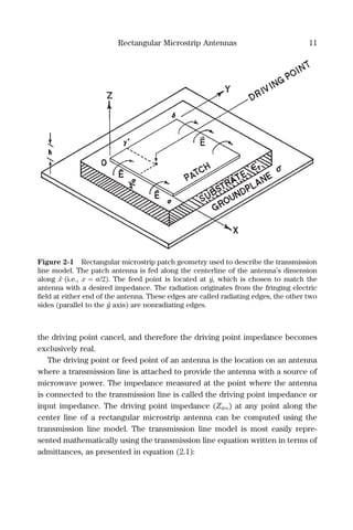
![16 Rectangular Microstrip Antennas
radiation pattern. The impedance of a typical resonant rectangular (a < 2b)
microstrip antenna at a radiating edge is around 200 Ω. This edge resistance
Rin is 1/(2Ge) at resonance. In general, one must provide an impedance trans-
formation to 50 Ω for this feed method. This is often accomplished using a
quarter-wave impedance transformer between the radiating edge impedance
and a 50 Ω microstrip feed line. A quarter-wave transformer has a larger band-
width than the antenna element and therefore does not limit it. It is possible
to widen a rectangular microstrip antenna (a > b) so the edge resistance at
resonance is 50 Ω. In this special case, no impedance transformer is required
to feed the antenna with a 50 Ω microstrip transmission line at a radiating
edge.
A fourth feed method, illustrated in Figure 2-3(d), is to cut a narrow notch
out of a radiating edge far enough into the patch to locate a 50 Ω driving point
impedance. The removal of the notch perturbs the patch fields. A study by
Basilio et al. indicates that a probe fed patch antenna has a driving point resis-
tance that follows an Rincos2
(πL2/L), while a patch with an inset feed is mea-
sured to follow an Rincos4
(πL2/L) function, where 0 < L2 < L/2.[11]
One can
increase the patch width, which increases the edge conductance, until at reso-
nance the edge impedance is 50 Ω. The inset distance into the patch goes to
zero, which allows one to directly feed a patch for this special case using a
50 Ω microstrip line at a radiating edge. The patch width is large enough in this
case to increase the antenna gain considerably.
Equation (2.8) may be used to compute the resonant length (L) of a rectan-
gular microstrip antenna:
L
c
f
l
l
r e
e
= −
= −
2
2
2
2
ε
λε
∆
∆ (2.8)
λ
λ
ε
εe
e
= 0
(2.9)
Equation (2.2) provides a predicted input impedance at the desired design
frequency fr. Numerical methods for obtaining the roots of an equation such](https://image.slidesharecdn.com/1891121731microstrip-151111163821-lva1-app6892/85/1891121731-microstrip-24-320.jpg)
![Rectangular Microstrip Antennas 17
as the Bisection Method (Appendix B) may be used with equation (2.2) to
determine the value of L1 and L2, which correspond to a desired input resis-
tance value. The initial guesses are along b at b1 = 0 (Rin = 1/2Ge) and b2 = b/2
(Rin ≈ 0).
The predicted position of a desired driving point impedance to feed the
antenna is generally close to measurement as long as the substrate height is
not larger than about 0.1λ0. A good rule of thumb for an initial guess to the
location of a 50 Ω feed point when determining the position in an empirical
manner is 1/3 of the distance from the center of the antenna to a radiating edge,
inward from a radiating edge.
Early investigation of the rectangular microstrip antenna, viewed as a linear
transmission line resonator, was undertaken by Derneryd.[12]
The input imped-
ance characteristics of the transmission line model were altered by Derneryd
in a manner which allows for the influence of mutual conductance between
the radiating edges of the patch antenna. This model further allows for the
inclusion of higher order linear transmission line modes.
In 1968, an experimental method to investigate the electric fields near sur-
rounding objects was developed which used a liquid crystal sheet backed with
a resistive thin film material.[13,14]
Derneryd used a liquid crystal field detector
of this type to map the electric field of a narrow microstrip antenna. Derneryd’s
results are reproduced in Figure 2-4, along with thermal (electric field magni-
tude) plots produced using the finite difference time domain (FDTD) method.
The FDTD patch analysis used a = 10.0 mm, b = 30.5 mm, εr = 2.55, h = 1.5875 mm
(0.0625 inches), and tan δ = 0.001. The feed point location is 5.58 mm from the
center of the patch antenna along the centerline. The groundplane is 20 mm ×
42 mm.
Figure 2-4(a) is the antenna without an electric field present. Figure 2-4(b)
is Derneryd’s element analyzed with a thermal liquid crystal display (LCD)
which shows the first (lowest order) mode of this antenna. The frequency for
this first mode is reported to be 3.10 GHz. A sinusoidal source at 3.10 GHz with
FDTD was used to model this antenna. The FDTD plot is of the total magnitude
of the electric field in the plane of the antenna. The FDTD simulation thermal
plot is very similar to the shape of the measured LCD thermal pattern. We see
two radiating edges at either end of the antenna in the lowest mode, with two
nonradiating edges on the sides.](https://image.slidesharecdn.com/1891121731microstrip-151111163821-lva1-app6892/85/1891121731-microstrip-25-320.jpg)
![18 Rectangular Microstrip Antennas
Figure 2-4(c) has Derneryd’s measured LCD results with the antenna driven
at 6.15 GHz. The LCD visualization shows the next higher order mode one
would expect from transmission line theory. The electric field seen at either
side of the center of the patch antenna along the nonradiating edges still con-
tribute little to the antenna’s radiation. In the far field, the radiation contribu-
Figure 2-4 Electric field distribution surrounding a narrow patch antenna as com-
puted using FDTD analysis and measured using a liquid crystal sheet: (a) patch without
fields, (b) 3.10 GHz, (c) 6.15 GHz, and (d) 9.15 GHz. After Derneryd [12].](https://image.slidesharecdn.com/1891121731microstrip-151111163821-lva1-app6892/85/1891121731-microstrip-26-320.jpg)
![Rectangular Microstrip Antennas 19
tions from each side of the nonradiating edges cancel.* The FDTD thermal plot
result in Figure 2-4(c) is once again very similar in appearance to Derneryd’s
LCD thermal measurement at 6.15 GHz.
The next mode is reported by Derneryd to exist at 9.15 GHz. The measured
LCD result in Figure 2-4(d) and the theoretical FDTD thermal plot once again
have good correlation. As before, the radiation from the nonradiating edges
will cancel in the far field.
The LCD method of measuring the near fields of microstrip antennas is still
used, but other photographic and probe measurement methods have been
developed as an aid to the visualization of the fields around microstrip
antennas.[15–18]
2.2 The Cavity Model
The transmission line model is conceptually simple, but has a number of draw-
backs. The transmission line model is often inaccurate when used to predict
the impedance bandwidth of a rectangular microstrip antenna for thin sub-
strates. The transmission line model also does not take into consideration the
possible excitation of modes which are not along the linear transmission line.
The transmission line model assumes the currents flow in only one direction
along the transmission line. In reality, currents transverse to these assumed
currents can exist in a rectangular microstrip antenna. The development of the
cavity model addressed these difficulties.
The cavity model, originated in the late 1970s by Lo et al., views the rectan-
gular microstrip antenna as an electromagnetic cavity with electric walls at the
groundplane and the patch, and magnetic walls at each edge.[19,20]
The fields
under the patch are the superposition of the resonant modes of this two-
* The far field of an antenna is at a distance from the antenna where a transmitted
(spherical) electromagnetic wave may be considered to be planar at the receive
antenna. This distance R is generally accepted for most practical purposes to be
R ≥
2 2
d
λ
. The value d is the largest linear dimension of transmit or receive antenna and
λ is the free-space wavelength. The near field is a distance very close to an antenna where
the reactive (nonradiating) fields are very large.](https://image.slidesharecdn.com/1891121731microstrip-151111163821-lva1-app6892/85/1891121731-microstrip-27-320.jpg)
![20 Rectangular Microstrip Antennas
dimensional radiator. (The cavity model is the dual of a very short piece of
rectangular waveguide which is terminated on either end with magnetic walls.)
Equation (2.10) expresses the (Ez) electric field under the patch at a location
(x,y) in terms of these modes. This model has undergone a considerable
number of refinements since its introduction.[21,22]
The fields in the lossy cavity
are assumed to be the same as those that will exist in a short cavity of this
type. It is assumed that in this configuration, where (h << λ0), only a vertical
electric field will exist (Ez) which is assumed to be constant along zˆ, and only
horizontal magnetic field components (Hx and Hy) exist. The magnetic field is
transverse to the zˆ axis (Figure 2-5) and the modes are described as TMmn
modes (m and n are integers). The electric current on the rectangular patch
antenna is further assumed to equal zero normal to each edge. Because the
electric field is assumed to be constant along the zˆ direction, one can multiply
equation (2.10) by h to obtain the voltage from the patch to the groundplane.
The driving point current can be mathematically manipulated to produce the
ratio of voltage to current on the left side of equation (2.10). This creates an
Figure 2-5 Rectangular microstrip patch geometry used for cavity model analysis.](https://image.slidesharecdn.com/1891121731microstrip-151111163821-lva1-app6892/85/1891121731-microstrip-28-320.jpg)
![Rectangular Microstrip Antennas 21
expression which can be used to compute the driving point impedance [equa-
tion (2.15)] at an arbitrary point (x´,y´), as illustrated in Figure 2-5.
E A x yz mn mn
nm
=
=
∞
=
∞
∑∑ Φ ( ),
00
(2.10)
A j
J
k k
mn
z mn
mn mn c mn
=
< >
< > −
ωµ
,
,
Φ
Φ Φ
1
2 2
(2.11)
Φmn
eff eff
x y
m x
a
n y
b
( ) cos cos, =
π π
(2.12)
The cavity walls are slightly larger electrically than they are physically due
to the fringing field at the edges, therefore we extend the patch boundary
outward and the new dimensions become aeff = a + 2∆ and beff = b + 2∆, which
are used in the mode expansion. The effect of radiation and other losses is
represented by lumping them into an effective dielectric loss tangent [equation
(2.19)].
k j kc r eff
2
0
2
1= −ε δ( ) (2.13)
k
m
a
n
b
mn
eff eff
2
=
+
π π
(2.14)
The driving point impedance at (x´,y´) may be calculated using
Z
j
j
drv
mn
mn effnm
=
− −=
∞
=
∞
∑∑
ωα
ω δ ω2 2
00 1( )
(2.15)
ω
ε
mn
mn
r
c k
= 0
(2.16)
α
δ δ
ε ε
π π
mn
m n
eff eff r eff eff
h
a b
m x
a
n y
b
=
0
2 2
cos cos s
′ ′
iinc2
2
m w
a
p
eff
π
(2.17)](https://image.slidesharecdn.com/1891121731microstrip-151111163821-lva1-app6892/85/1891121731-microstrip-29-320.jpg)
![22 Rectangular Microstrip Antennas
wp is the width of the feed probe.
δi
i
i
=
=
≠{1 0
2 0
if
if
(2.18)
The effective loss tangent for the cavity is computed from the total Q of the
cavity.
δeff
T d c r swQ Q Q Q Q
= = + + +
1 1 1 1 1
(2.19)
The total quality factor of the cavity QT consists of four components: Qd, the
dielectric loss; Qc, the conductor loss; Qr, the radiation loss; and Qsw, the
surface wave loss.
Qd =
1
tanδ
(2.20)
Q
k h
R
c r
s
=
1
2
0
0
η µ (2.21)
R
w
s =
µ
σ
0
2
(2.22)
Q
wW
P
r
es
r
=
2
(2.23a)
where Wes is the energy stored:
W
abV
h
es
r
=
ε ε0 0
2
8
(2.23b)
The power radiated into space is Pr.[23]
P
V A
B
A A B A A
r = − − +
+ − +
0
2 4 2 2 2
23040
1 1
15 420 5
2
7 189
π
( )
(2.24)](https://image.slidesharecdn.com/1891121731microstrip-151111163821-lva1-app6892/85/1891121731-microstrip-30-320.jpg)
![Rectangular Microstrip Antennas 23
A
a
=
π
λ0
2
(2.25a)
B
b
=
2
0
2
λ
(2.25b)
V0 is the input (driving point) voltage.
The Q of the surface wave loss (Qsw) is related to the radiation quality
factor (Qr):[24]
Q Q
e
e
sw r
r
hed
r
hed
=
−
1
(2.26)
e
P
P P
r
hed r
hed
r
hed
sw
hed
=
+
(2.27)
P
k h c
r
hed r
=
( ) ( )0
2 2 2
1
0
2
80π µ
λ
(2.28a)
c
n n
1
1
2
1
4
1
1 2
5
= − + (2.28b)
n r r1 = ε µ (2.29)
P
k x
x k h x x
sw
hed r
r r
=
−
+ + − +
η ε
ε ε
0 0
2
0
2 3 2
1 0 0
2 2
1
8
1
1 1 1
( )
( ) ( )
(2.30)
x
x
xr
1
0
2
0
2
1
=
−
−ε
(2.31)
x r r r
r
0
2
0 1
2
0 1 0
2
2
1
2
1
2
= +
− + + − +
−
ε α α ε ε α α α
ε α( )
(2.32)
α ε ε0 01 1= − −r rk htan( ) (2.33)](https://image.slidesharecdn.com/1891121731microstrip-151111163821-lva1-app6892/85/1891121731-microstrip-31-320.jpg)
![24 Rectangular Microstrip Antennas
α
ε
ε
ε
ε
1
0
0
2
0
1
1
1
1
= −
− +
−
−
−
tan( )
cos ( )
k h
k h
k h
r
r
r
r
(2.34)
The cavity model is conceptually accessible and readily implemented, but
its accuracy is limited by assumptions and approximations that are only valid
for electrically thin substrates. The self-inductance of a coaxial probe used to
feed the rectangular microstrip antenna is not included in this model. The
cavity model is generally accurate in its impedance prediction and is within 3%
of measured resonant frequency for a substrate thickness of 0.02λ0 or less.
When it is thicker than this, anomalous results may occur.[25]
2.2.1 The TM10 and TM01 Mode
When a rectangular microstrip antenna has its dimension a wider than dimen-
sion b and is fed along the centerline of dimension b, only the TM10 mode may
be driven. When it is fed along the centerline of dimension a, only the TM01
mode may be driven.
When the geometric condition a > b is met, the TM10 mode is the lowest
order mode and possesses the lowest resonant frequency of all the time har-
monic modes. The TM01 mode is the next highest order mode and has the next
lowest resonant frequency (Figure 2-6).
When b > a, the situation is reversed, TM01 becomes the mode with the
lowest resonant frequency and TM10 has the next lowest resonant frequency.
If a = b, the two modes TM10 and TM01 maintain their orthogonal nature, but
have identical resonant frequencies.
The integer mode index m of TMmn is related to half-cycle variations of the
electric field under the rectangular patch along a. Mode index n is related to
the number of half-cycle electric field variations along b. In the case of the TM10
mode, the electric field is constant across any slice through b (i.e., the yˆ direc-
tion) and a single half-cycle variation exists in any cut along a (i.e., the xˆ direc-
tion). Figure 2-4 shows a narrow patch driven in the TM01, TM02, and TM03
modes according to cavity model convention.](https://image.slidesharecdn.com/1891121731microstrip-151111163821-lva1-app6892/85/1891121731-microstrip-32-320.jpg)
![Rectangular Microstrip Antennas 25
One notes that the electric field is equal to zero at the center of a rectangular
patch for both the TM10 and TM01 modes. This allows a designer the option of
placing a shorting pin in the center of the rectangular patch without affecting
the generation of either of the two lowest order modes. This shorting pin or
via forces the groundplane and rectangular patch to maintain an equivalent
direct current (DC) electrostatic potential. In many cases the buildup of static
charge on the patch is undesirable from an electrostatic discharge (ESD) point
of view, and a via may be placed in the center of the rectangular patch to
address the problem.
Figure 2-7(a) shows the general network model used to represent a rectan-
gular microstrip antenna. The TM00 mode is the static (DC) term of the series.[26]
As described previously, the TM10 and/or TM01 are the two lowest order modes
that are generally driven in most applications. When this is the case, the other
higher order modes are below cut-off and manifest their presence as an infinite
Figure 2-6 When a > b, the TM10 mode is the lowest order mode (lowest resonant
frequency) for a rectangular microstrip antenna. The TM01 mode has the next highest
resonant frequency.](https://image.slidesharecdn.com/1891121731microstrip-151111163821-lva1-app6892/85/1891121731-microstrip-33-320.jpg)

![Rectangular Microstrip Antennas 27
patch increases, the contribution of the equivalent series inductance of the
higher order modes to the driving point impedance becomes larger and larger,
which produces a larger and larger mismatch, until the patch antenna can no
longer be matched by simply choosing an appropriate feed point location. The
cavity model does not include the small amount of intrinsic self-inductance
introduced by a coaxial feed probe.[27]
Increasing the thickness of the substrate
also increases the impedance bandwidth of the element. These two properties
(impedance bandwidth and match) may need to be traded off in a design.
The cavity model is accurate enough to use for many engineering designs.
Its advantage is that it is expressed with closed form equations, which allow
efficient computation and ease of implementation. Its disadvantage is its
accuracy when compared with more rigorous methods.
The cavity model equations presented previously were implemented
for a rectangular patch antenna with a = 34.29 mm and a resonant length of
b = 30.658 mm (TM01). The feed point is 7.595 mm from the center of the patch,
Figure 2-8 Comparison to measurement of predicted negative return loss of a rect-
angular microstrip patch (of parameters in Table 2-1) by the cavity model and FDTD
analysis.](https://image.slidesharecdn.com/1891121731microstrip-151111163821-lva1-app6892/85/1891121731-microstrip-35-320.jpg)


![30 Rectangular Microstrip Antennas
have this spacing in free space, the array produces a maximum directivity.
As the dielectric constant increases, the resonant length of the patch along
a decreases, which decreases the spacing between the radiating slots. The
slots no longer optimally add broadside to the rectangular microstrip antenna,
which decreases the directivity and hence increases the pattern beamwidth.
The electric field from a single slot with a voltage across the slot of V0 is
given as[28]
E j V bk
e
r
F
jk r
φ
π
θ φ= −
−
2
4
0 0
0
( ), (2.35)
Eθ = 0 (2.36)
F
k h
k h
k b
( )
sin( ( / )sin cos )
( / )sin cos
sin( ( / )cos
θ φ
θ φ
θ φ
θ
, = ⋅0
0
02
2
2 ))
( / )cos
sin
k b0 2 θ
θ (2.37)
k0
0
2
=
π
λ
(2.38)
For two slots spaced at a distance a apart, the E-plane radiation pattern is
F
k h
k h
k bE( )
sin( ( / )cos )
( / )cos
cos( / cos )φ
φ
φ
φ= 0
0
0
2
2
2 (2.39)
The H-plane pattern is independent of the slot spacing a and is given by
F
k b
k b
H( )
sin( cos )
cos
sinθ
θ
θ
θ= 0
0
(2.40)
The angle θ is measured from the zˆ axis and φ is measured from the xˆ axis.
The directivity of a microstrip antenna can be approximated by starting with
the directivity of a single slot:[29]
D
b
I
=
4 2 2
1 0
2
π
λ
(2.41)](https://image.slidesharecdn.com/1891121731microstrip-151111163821-lva1-app6892/85/1891121731-microstrip-38-320.jpg)


![Rectangular Microstrip Antennas 33
surface equivalence theorem.[30,31]
One can see the measured and FDTD results
are very similar for the upper hemisphere in both the E- and H-plane patterns.
Equation (2.43) was used to compute the directivity for the slot model. The E-
plane slot model pattern results are close for ±45º, but begin to deviate at low
angles. The H-plane slot model is close up to about ±60º. The slot model does
not take groundplane affects into account, but is clearly very accurate consid-
ering the simple model used.
The important parameter which determines the directivity of a microstrip
antenna is the relative dielectric constant εr of the substrate. When the sub-
strate is air (εr ≈ 1.0), the two antenna edges are approximately half of a free
space wavelength apart (λ0/2). This spacing produces an array spacing for the
slot model which produces maximum directivity. It is possible to achieve a
directivity of almost 10 dB with an air loaded rectangular microstrip patch
antenna. As the dielectric constant of the substrate is increased, the slots
become closer in terms of free space wavelengths and no longer array to
produce as high a directivity as in the free space case. As the substrate dielec-
tric constant of a rectangular microstrip antenna increases, the directivity of
a patch antenna decreases. Table 2-3 presents a comparison of the directivity
predicted by the slot model and FDTD method for a square microstrip antenna.
For low values of relative dielectric constant (εr < 4.0), the slot model is within
approximately 1 dB. For εr > 4.0, the directivity of the slot model is still within
about 1.5 dB. The slot model can be useful for estimating directivity.
Table 2-3 Directivity (dB) of a square linear microstrip
antenna vs. εr (2.45 GHz, h = 3.048 mm, tanδ = 0.0005).
εr Slot Model FDTD
1.0 8.83 8.00
2.6 6.56 7.11
4.1 5.93 6.82
10.2 5.24 6.54
20.0 5.01 6.45
Square Groundplane Dimensions for FDTD = 63.5 mm ×
63.5 mm
(Antenna Centered)](https://image.slidesharecdn.com/1891121731microstrip-151111163821-lva1-app6892/85/1891121731-microstrip-41-320.jpg)
![34 Rectangular Microstrip Antennas
2.4 Quarter-Wave Rectangular Microstrip Antenna
Understanding the electric field distribution under a rectangular microstrip
antenna allows us to develop useful variations of the original λ/2 rectangular
microstrip antenna design. In the case where a microstrip antenna is fed to
excite the TM01 mode exclusively, a virtual short-circuit plane exists in the
center of the antenna parallel to the x axis centered between the two radiating
edges. This virtual shorting plane can be replaced with a physical metal short-
ing plane to create a rectangular microstrip antenna that is half of its original
length (approximately λeff/4), as illustrated in Figure 2-11. Only a single radiat-
ing edge remains with this design, which reduces the radiation pattern directiv-
ity compared with a half-wavelength patch. This rectangular microstrip antenna
design is known as a quarter-wave microstrip patch or half-patch antenna. The
use of a single shorting plane to create a quarter-wave patch antenna was first
described by Sanford and Klein in 1978.[32]
Later, Post and Stephenson[33]
Figure 2-11 A quarter-wave microstrip antenna has a shorting wall which replaces
the virtual short found in a half-wave microstrip antenna.](https://image.slidesharecdn.com/1891121731microstrip-151111163821-lva1-app6892/85/1891121731-microstrip-42-320.jpg)
![Rectangular Microstrip Antennas 35
described a transmission line model to predict the driving point impedance of
a λ/4 microstrip antenna.
The length of a quarter-wavelength patch antenna for a given operating
frequency fr is
L
c
f
l
r e
= −
4 ε
∆ (2.47)
= −
λεe
l
4
∆ (2.48)
Y Y
Y jY L
Y jY L
jY Ldrv
e
e
=
+
+
−0
0 2
0 2
0 1
tan( )
tan( )
cot( )
β
β
β (2.49)
The transmission line model of a quarter-wave microstrip antenna is pre-
sented in Figure 2-12. Equation (2.49) represents the driving point admittance
at a point along L represented by L = L1 + L2. The final term in equation (2.49)
is a pure susceptance at the driving point which is due to the shorted transmis-
sion line stub. The admittance at the driving point from the section of transmis-
sion line that translates the edge admittance Ye along a transmission line of
length L2 resonates when its susceptance cancels the susceptance of the
shorted stub. The 50 Ω input resistance location may be found from equation
(2.49), with an appropriate root finding method such as the bisection method
(Appendix B). The 50 Ω driving point impedance location is not exactly at the
same position relative to the center short as the 50 Ω driving point location of
a half-wavelength patch is to its virtual shorting plane. This is because, for the
case of the half-wavelength patch, two radiators exist and have a mutual cou-
pling term that disappears in the quarter-wavelength case. Equation (2.49) does
not take this difference into account, but provides a good engineering starting
point. This change in mutual coupling also affects the cavity Q, which in turn
reduces the impedance bandwidth of a quarter-wavelength patch to approxi-
mately 80% of the impedance bandwidth of a half-wavelength patch.[34]
The short circuit of the quarter-wave patch antenna is critical. To maintain
the central short, considerable current must exist within it. Deviation from a
low impedance short circuit will result in a significant change in the resonant](https://image.slidesharecdn.com/1891121731microstrip-151111163821-lva1-app6892/85/1891121731-microstrip-43-320.jpg)
![36 Rectangular Microstrip Antennas
frequency of the antenna and modify the radiation characteristics.[35]
A design
of this type often uses a single piece of metal with uniform width which is
stamped into shape and utilizes air as a dielectric substrate.
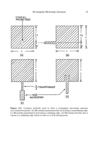
2.5 λ/4 × λ/4 Wavelength Rectangular Microstrip Antenna
When a = b, the TM01 and TM10 modes have the same resonant frequency
(square microstrip patch). If the patch is fed along the diagonal, both modes
can be excited with equal amplitude and in phase. This causes all four edges
to become radiating edges. The two modes are orthogonal and therefore inde-
Ydrv
L1
jBe Ge
L2
Ydrv
L1
Yo Yo
L2
Ye
L
Figure 2-12 Transmission line model of a quarter-wave microstrip antenna.](https://image.slidesharecdn.com/1891121731microstrip-151111163821-lva1-app6892/85/1891121731-microstrip-44-320.jpg)
![Rectangular Microstrip Antennas 37
pendent. Because they are in phase, the resultant of the electric field radiation
from the patch is slant linear along the diagonal of the patch.
When a square microstrip patch is operating with identical TM01 and TM10
modes, a pair of shorting planes exist centered between each of the pairs of
radiating slots (Figure 2-13). We can replace the virtual shorting planes, which
divide the patch into four sections, with physical shorting planes. We can
remove one section (i.e., quadrant) and drive it separately due to the symmetry
of the modes (Figure 2-14). This produces an antenna that has one-fourth the
area of a square patch antenna.[36]
This provides a design option for applica-
tions where volume is restricted.
Figure 2-13 Development of a λ/4-by-λ/4 microstrip antenna from a square microstrip
antenna. When a square microstrip antenna is driven along the diagonal, two virtual
shorting planes appear. Replacing the virtual shorting planes with physical shorting
planes allows one to remove a quarter section of the original antenna and drive it
independently.](https://image.slidesharecdn.com/1891121731microstrip-151111163821-lva1-app6892/85/1891121731-microstrip-45-320.jpg)

![40 Rectangular Microstrip Antennas
the modes to have a 90º phase difference. This situation is the most general
geometry describing this type of circularly polarized patch. One could use a
single tab, a single indent, a pair of tabs, or a pair of indents to perturb a rect-
angular microstrip antenna and produce circular polarization.
The third method illustrated in Figure 2-15(III) is to remove a pair of corners
from the microstrip antenna. This creates a pair of diagonal modes (no longer
TM10 and TM01 as the shape of the patch has been altered) that can be adjusted
to have identical magnitudes and a 90º phase difference between these modes.
The fourth method in Figure 2-15(IV) is to place a slot diagonally across the
patch. The slot does not disturb the currents flowing along it, but electrically
lengthens the patch across it. The dimensions of the slot can be adjusted to
produce circular polarization. It is important to keep the slot narrow so that
radiation from the slot will be minimal. One only wishes to produce a phase
shift between modes, not create a secondary slot radiator. Alternatively, one
can place the slot across the patch and feed along the diagonal.[37]
Figure 2-16 illustrates how one designs a patch of type I. Figure 2-16(a)
shows a perfectly square patch antenna probe fed in the lower left along
the diagonal. This patch will excite the TM10 and TM01 modes with identical
amplitudes and in phase. The two radiating edges which correspond to each
of the two modes have a phase center that is located at the center of the
patch. Therefore the phase center of the radiation from the TM10 and TM01
modes coincide and are located in the center of the patch. When a = b, the
two modes will add in the far field to produce slant linear polarization
along the diagonal. If the aspect ratio of the patch is changed so that a > b, the
resonant frequency of each mode shifts. The TM10 mode shifts down in fre-
quency and the TM01 mode shifts up compared with the original resonant
frequency of the slant linear patch. Neither mode is exactly at resonance.
This slightly nonresonant condition causes the edge impedance of each mode
to possess a phase shift. When the phase angle of one edge impedance is +45º
and the other is −45º, the total difference of phase between the modes is 90º.
This impedance relationship clearly reveals itself when the impedance versus
frequency of the patch is plotted on a Smith chart. The frequency of optimum
circular polarization is the point on a Smith chart which is the vertex of a
V-shaped kink.
Figure 2-17 presents the results of a cavity model analysis of a patch radiat-
ing left-hand circular polarization (LHCP) using a rectangular microstrip](https://image.slidesharecdn.com/1891121731microstrip-151111163821-lva1-app6892/85/1891121731-microstrip-48-320.jpg)

![42 Rectangular Microstrip Antennas
antenna with an appropriate a/b ratio. The antenna operates at 2.2 GHz, its
substrate thickness is 1.5748 mm, with εr = 2.5, tan δ = 0.0019, a = 40.945 mm,
and b = 42.25 mm. The patch is fed at x´ = 13.5 mm, y´ = 14.5 mm, and Wp =
1.3 mm. The approximate a/b ratio was arrived upon using trial and error with
equation (2.54).
The design of a rectangular circularly polarized patch is difficult to realize
due to the sensitivity of the patch to physical dimensions and dielectric con-
stant. One method is to start with the case of the slant linear patch. The slant
linear patch has a = b and is therefore square and has its dimensions chosen
to produce resonance at a desired design frequency. The ratio of a/b when the
square patch aspect ratio has been adjusted to produce circular polarization
has been derived using a perturbation technique:[38]
a
b Q
= +1
1
0
(2.50)
The Q of the unperturbed slant linear patch (Q0) is given by
1 1 1 1 1
0Q Q Q Q Qd c r sw
= + + + (2.51)
The Q of a square rectangular microstrip antenna driven as a slant linear patch
or as a linear patch are essentially identical. When a patch is square, the TM10
and TM01 modes are degenerate, the energy storage in the TM10 and TM01 modes
are identical, as is the amount of energy loss in each for the slant linear case.
If all the energy is stored in a single TM10 or TM01, as occurs when the patch is
driven in the linear case, the same total amount of energy will be lost as in the
slant linear case. In both situations, the energy stored per cycle versus energy
lost is the same, and therefore so is the Q.
If the slant linear patch has the dimension á (= b´), the new dimensions of
the circularly polarized patch will be
a a L= ′ + ∆ (2.52a)
b a L= ′ − ∆ (2.52b)](https://image.slidesharecdn.com/1891121731microstrip-151111163821-lva1-app6892/85/1891121731-microstrip-50-320.jpg)

![44 Rectangular Microstrip Antennas
The driving point impedance of the slant linear patch and the patch modified
to have circular polarization using the a and b values computed with equation
(2.52a) and equation (2.52b) are plotted in Figure 2-18. Again, the cavity model
has been used to compute the driving point impedance. It can be seen that
in this case the computation has the advantage that it produces a better
match for the circularly polarized patch which has been modified to produce
circular polarization than the trial and error method of the original patch.
The input impedance at 2.2 GHz for the patch modified to produce circular
polarization is 46.6 + j1.75 Ω. This is about half the input resistance value
of the slant linear patch. This calculation provides some insight into the sen-
sitivity of the driving point impedance location of the design to physical para-
meters of the patch.
The cavity model can be used to compute the axial ratio of a circularly
polarized rectangular patch.[39]
The relationship between electric field and axial
ratio is[40]
Figure 2-18 The rectangular patch antenna of Figure 2-17 has its dimensions aver-
aged to create a slant linear patch which resonates at 2.2 GHz using cavity model analy-
sis (dashed lines). Next, equation (2.52a) and equation (2.52b) are used to compute the
values of a and b required to produce circular polarization at 2.2 GHz, which is then
analyzed using the cavity model (solid lines).](https://image.slidesharecdn.com/1891121731microstrip-151111163821-lva1-app6892/85/1891121731-microstrip-52-320.jpg)

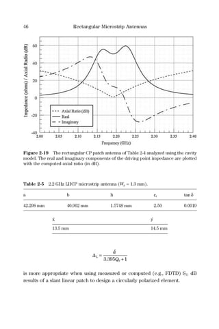
![Rectangular Microstrip Antennas 47
Equation (2.53) also shows that as the antenna Q increases, ∆L decreases.
When a high dielectric constant is used as a substrate, the Q of the antenna
becomes larger, which means the impedance bandwidth has become narrower.
The high dielectric constant also decreases the size of the patch, which
drives down the value of ∆L, which tightens any manufacturing tolerances
considerably.
A more complex iterative approach that uses the cavity model to compute
single-feed circularly polarized rectangular patch designs is presented by
Lumini et al.[41]
Another design approach is to use a genetic algorithm optimi-
zation with the cavity model to develop a circularly polarized rectangular
microstrip antenna design.[42]
This method has the advantage that it optimizes
for driving point match and axial ratio simultaneously. This eliminates first
developing a slant linear patch and then using equation (2.52a) and equa-
tion (2.52b) to compute the dimensions to produce circular polarization.
Experience with genetic algorithms indicates that it produces a design which
is no better than the more straightforward method previously described.
Figure 2-15(II) uses indentation tabs to produce circular polarization. This
type of design is undertaken experimentally.
Figure 2-15(III) has a pair of corners cut off to produce circular polarization.
This creates a pair of diagonal modes (no longer TM10 and TM01, as the shape
of the patch has been altered) that can be adjusted to have identical magni-
tudes and a 90º phase difference between these modes. The antenna is fed
along the centerline in this case so it will excite each of the diagonal modes
with equal amplitude. In Figure 2-15 we see that if the upper right-hand corner
and lower left-hand corner are reduced, we can view the situation as reducing
the capacitance along that diagonal, making it more inductive. The opposite
diagonal from lower right to upper left remains unchanged and has a larger
capacitance by comparison. The amount of the area removed can be adjusted
so the phase of the chopped corner diagonal is 45º and the phase of the unmodi-
fied diagonal is −45º. This situation creates right-hand circular polarization
(RHCP). Leaving the feed point position unchanged and removing the opposite
pair of corners reverses the phase, and thus the polarization sense.
We will define the total area removed to perturb the patch so it produces
circular polarization as ∆S (Figure 2-15). The total area S of the unperturbed
square patch prior to the corner removal to produce circular polarization is](https://image.slidesharecdn.com/1891121731microstrip-151111163821-lva1-app6892/85/1891121731-microstrip-55-320.jpg)
![48 Rectangular Microstrip Antennas
S = a · b = á2
(a = b = á). It has been reported that the ratio of the change in
area ∆S to the original area of the patch S is related to the Q of the uncut
antenna Q0 computed using equation (2.51) by[43]
∆S
S Q
=
1
2 0
(2.58)
The area to be cut from each corner of the unperturbed patch, as shown in
Figure 2-15(III), is half of the perturbation area S calculated using equation
(2.58) or ∆S/2S. In terms of the length along each edge which is cut off we have
∆L
a
Q
=
′
0
(2.59)
Figure 2-15(IV) uses a diagonal slot to produce circular polarization. A
guideline for choosing the slot area is to make it equal to ∆S/S.
45° –45° –45° 45°
RHCP LHCP
Figure 2-20 One may cut off a pair of opposing corners of a rectangular microstrip
antenna to produce circular polarization. One can view cutting off a corner as reducing
the capacitance of that diagonal mode. This will produce a more inductive impedance
across the two chopped corners which will cause the electric field to have a phase of
45º compared with the −45º of the electric field with the capacitive impedance across
the uncropped corners. Reversing the position of the corners reverses the polarization
sense.](https://image.slidesharecdn.com/1891121731microstrip-151111163821-lva1-app6892/85/1891121731-microstrip-56-320.jpg)

![50 Rectangular Microstrip Antennas
2.6.3 Quadrature (90º) Hybrid
The design of a rectangular patch with circular polarization (Section 2.6.2)
requires a branchline hybrid, also known as a quadrature hybrid. A branchline
quadrature hybrid provides a 3 dB power split between a pair of output ports
with a 90º difference between them. The left-hand illustration of Figure 2-21(b)
shows a branchline hybrid as it would appear realized in stripline or microstrip.
The shunt branches have a characteristic impedance Zs and the through or
series branch has a characteristic impedance of Zt.
At the branchline hybrid design frequency, the scattering parameters
are[44]
S j
Z
Z
t
21
0
= − (2.60a)
Figure 2-21 (b) A 90º branchline hybrid realized in microstrip or stripline and as often
packaged commercially.](https://image.slidesharecdn.com/1891121731microstrip-151111163821-lva1-app6892/85/1891121731-microstrip-58-320.jpg)
![Rectangular Microstrip Antennas 51
S
Z
Z
t
s
31 = − (2.60b)
S11 0 0= . (2.60c)
S41 0 0= . (2.60d)
The illustration on the right of Figure 2-21(b) shows how a commercial
hybrid appears with coaxial connectors. Some hybrids have a built-in load on
one port, as shown, while others require the user to provide a load. This allows
one to have one input that produces RHCP and another that produces LHCP,
as shown in Figure 2-21(a). This allows a system to switch between polariza-
tion if desired.
When a 3 dB split between ports is desired with a reference impedance of
Z0 (generally 50 Ω), the shunt branches should have Zs = Z0 and the through
branches Zt = Z0/ 2 (35.4 Ω for a 50 Ω system). The lengths of the branches
are all λ/4. When port 1 is used as an input port, then port 2 receives half of
the input power and is the phase reference for port 3. Port 3 receives half of
the input port power with a phase that is 90º behind port 2. The split waves
cancel at port 4, which is called the isolated port. A load is generally placed
on this port to absorb any imbalance, which stabilizes the phase difference
between port 2 and 3. If port 4 is the input port, port 1 becomes the isolation
port, port 3 is the 0º phase port with half the power, and port 2 becomes the
−90º port.
In practice, there is often a slight imbalance in the power split between ports
2 and 3. We note that equation (2.60b) has Zs in its denominator. This allows
one to change the characteristic impedance of the shunt branches slightly and
obtain a more even power split.
The bandwidth of a branchline hybrid is limited by the quarter-wave length
requirement on the branches to 10–20%. One must also take the discontinuities
at the transmission line junctions into account to produce a design which
operates as desired. One can increase the bandwidth of a branchline coupler
by adding cascading sections.[45]
Recently Qing added an extra section to
produce a three-stub hybrid coupler and created a microstrip antenna design
with 32.3% 2:1 voltage standing wave ratio (VSWR) bandwidth and 42.6% 3 dB](https://image.slidesharecdn.com/1891121731microstrip-151111163821-lva1-app6892/85/1891121731-microstrip-59-320.jpg)
![52 Rectangular Microstrip Antennas
axial ratio bandwidth.[46]
Quadrature hybrids that have unequal power division
and/or unequal characteristic impedances at each port can also be
designed.[47]
2.7 Impedance and Axial Ratio Bandwidth
The impedance bandwidth of a rectangular microstrip antenna can be deter-
mined with the total Q used in the cavity model. For a linear rectangular
microstrip antenna, driven in a single mode, the normalized impedance band-
width is related to the total Q by[48]
BW
S
Q S
Linear
T
=
−1
(S:1 VSWR) (2.61)
When a linear microstrip antenna design is very close to achieving an imped-
ance bandwidth design goal, one can obtain a tiny amount of extra impedance
bandwidth by designing the antenna to have a 65 Ω driving point resistance at
resonance rather than a perfectly matched 50 Ω input resistance. The perfect
match at one frequency is traded for a larger overall 2:1 VSWR bandwidth.[49]
The impedance bandwidth also increases slightly when the width of the rect-
angular microstrip antenna is increased. The largest bandwidth increase occurs
as the substrate dielectric constant εr is decreased and/or the substrate thick-
ness is increased. The effect substrate thickness and dielectric constant have
on impedance bandwidth as computed with the cavity model is illustrated in
Figure 2-22 for a square linearly polarized microstrip antenna.
One must recall that as the substrate thickness is increased, higher order
modes provide a larger and larger contribution to an equivalent series induc-
tance, which in turn produces a larger and larger driving point mismatch. A
desirable driving point impedance must be traded for impedance bandwidth.
Equation (2.62) and equation (2.63) have been developed to relate the imped-
ance bandwidth of a rectangular patch antenna radiating circular polarization
to total Q as well as its expected axial ratio bandwidth. We can substitute
S = 2 in equation (2.61) and equation (2.62), forming the ratio of circular to
linear bandwidth. This reveals that the impedance bandwidth of a circularly](https://image.slidesharecdn.com/1891121731microstrip-151111163821-lva1-app6892/85/1891121731-microstrip-60-320.jpg)

![54 Rectangular Microstrip Antennas
where p is the fraction of power received by a matched load (load resistance
is equal to driving point resistance at resonance), to the power received by the
antenna at its resonant frequency (0 < p < 1). The received power reaches
maximum when p = 1 and becomes zero when p = 0. In equation (2.64), pmin is
the minimum acceptable receive power coefficient for a given design.
Langston and Jackson have written the above expressions in terms of a
normalized frequency variable for comparison.[50]
The axial ratio bandwidth
is the smallest for a transmitting single-feed circularly polarized patch.
The receive power bandwidth is larger than the axial ratio or impedance
bandwidth.
2.8 Efficiency
The antenna efficiency e relates the gain and directivity of an antenna:
G eD= (2.65)
where G is the antenna gain and D is directivity.
The efficiency of a rectangular microstrip antenna can be calculated from
the cavity model in terms of the cavity Qs.[51]
The radiated efficiency is the
power radiated divided by the total power, which is the sum of the radiated,
surface wave, conductor loss, and dielectric loss. The stored energy is identical
for all the cavity Qs. This allows us to write:
e
Q
Q
T
r
= (2.66)
which expanded out is
e
Q Q Q
Q Q Q Q Q Q Q Q Q Q Q Q
d c sw
sw c d sw c r sw r d r d c
=
+ + +
(2.67)
When multiplied by 100%, equation (2.66) gives the antenna efficiency in
percent as predicted by the cavity model. We can readily see from equation](https://image.slidesharecdn.com/1891121731microstrip-151111163821-lva1-app6892/85/1891121731-microstrip-62-320.jpg)

![56 Rectangular Microstrip Antennas
When the dielectric constant is increased to εr = 10.2 (Table 2-8), we see the
surface wave power increases significantly compared with the εr = 2.6 case in
Table 2-7. The thinnest substrate only radiates 53.75% into the space wave.
As h increases from 0.762 mm to 1.524 mm, the amount lost to the conductor
and dielectric loss approximately reverse contributions. The best compromise
to maximize the losses due to the space wave, and minimize the conductor and
dielectric losses, is the 2.286 mm thickness. Computing the losses separately
can be very useful to a designer when evaluating the choice of substrate thick-
ness for a given design. This is often a good design path to use because of the
difficulty involved in making experimental efficiency measurements.[52]
2.9 Design of a Linearly Polarized Microstrip Antenna with
Dielectric Cover
Microstrip antennas are often enclosed in dielectric covers (i.e., radomes) to
protect them from harsh environments. These can range from vacuum-molded
Table 2-7 Losses in a square linear microstrip antenna versus h (2.45 GHz, a =
b = 37.62 mm, tanδ = 0.0025, εr = 2.6).
h ηr ηsw ηc ηd
(0.030″) 0.762 mm 76.28% 2.43% 8.82% 12.47%
(0.060″) 1.524 mm 85.15% 5.43% 2.46% 6.96%
(0.090″) 2.286 mm 85.96% 8.25% 1.10% 4.68%
(0.120″) 3.048 mm 84.99% 10.93% 0.61% 3.47%
Table 2-8 Losses in a square linear microstrip antenna versus h (2.45 GHz, a = b =
19.28 mm, tanδ = 0.0025, εr = 10.2)
h ηr ηsw ηc ηd
(0.030″) 0.762 mm 53.75% 24.71% 17.47% 4.07%
(0.060″) 1.524 mm 68.09% 10.73% 5.53% 15.65%
(0.090″) 2.286 mm 69.31% 17.56% 2.50% 10.62%
(0.120″) 3.048 mm 66.27% 24.76% 1.35% 7.62%](https://image.slidesharecdn.com/1891121731microstrip-151111163821-lva1-app6892/85/1891121731-microstrip-64-320.jpg)
![Rectangular Microstrip Antennas 57
or injection-molded plastic enclosures which leave an air gap between the
radiating patch and the radome, to bonding a plastic material directly to the
antenna.
Bonding dielectric material directly to the antenna can provide a high degree
of hermetic sealing. When the substrate material is Teflon based, the bonding
process to produce good adhesion can be very involved. In some commercial
applications, the injection molding of a plastic radome which surrounds the
antenna element and seals it has been implemented. In these cases, the use of
a full-wave simulator such as Ansoft HFSS is best for the refinement of a
design prior to prototyping, but the use of a quick quasi-static analysis can
provide initial design geometry for refinement and design sensitivity prior to
optimization.
A number of approaches have been forwarded to analyze a microstrip
antenna with a dielectric cover.[53–56]
Here we will utilize the transmission line
model to analyze a rectangular microstrip antenna with a dielectric cover.
A quasi-static analysis of a microstrip transmission line with a dielectric
cover forms the basis of this analysis.[57]
An effective dielectric constant for
the geometry shown in Figure 2-23 is defined in equation (2.68) and the
characteristic impedance is related in equation (2.69).
ε ε
e
C
C
r
=
0
(2.68)
Z
Zair
e
0 =
ε
(2.69)
Z
cC
air =
1
0
(2.70)
where
εe = effective dielectric constant of microstrip line
Z0 = characteristic impedance of microstrip line
Zair = characteristic impedance of microstrip line with no dielectrics
present](https://image.slidesharecdn.com/1891121731microstrip-151111163821-lva1-app6892/85/1891121731-microstrip-65-320.jpg)
![58 Rectangular Microstrip Antennas
Cεr
= capacitance per unit length with dielectrics present
C0 = capacitance per unit length with only free space present
c = speed of light in a vacuum.
Using the substitution of α = βh1 in Bahl et al.[58]
, we are able to write the
capacitance as
1 1
1 6
2
2
2 4 2
2
0
1
1
1
2
0C
W h
W h
W h
W
= +
⋅−
∞
∫πε
α
α
α
α
.
sin( / )
( / )
. ( / )
cos( / hh
W h
W h
W h W h1
1
1
2
1 1
22 2
2
4 4)
sin( / )
( / )
sin ( / ) ( / )− + ⋅
−α
α
α α
22
⋅
ε
ε α
ε α
ε α αr
r
r
r
h h
h h2
2
2
1
2 1
2 1
1tanh( / )
tanh( / )
coth( )
+
+
+
−1
dα (2.71)
Figure 2-23 Rectangular microstrip patch geometry of a dielectric covered microstrip
antenna analyzed with the transmission line model. The patch antenna is fed along
the centerline of the antenna’s width (i.e., W/2). The feed point is represented by the
black dot.](https://image.slidesharecdn.com/1891121731microstrip-151111163821-lva1-app6892/85/1891121731-microstrip-66-320.jpg)
![Rectangular Microstrip Antennas 59
where
W = width of microstrip transmission line (patch width)
h1 = thickness of dielectric substrate
εr1 = relative dielectric constant of substrate
h2 = thickness of dielectric superstrate (dielectric cover/radome)
εr2 = relative dielectric constant of radome dielectric superstrate (dielectric
cover/radome).
The integration of equation (2.71) is efficiently computed using Gaussian
quadrature, as presented in Appendix B. The slot admittance is modified when
a dielectric cover is added to a rectangular microstrip antenna design. The
modification is slight and is best computed using equation (2.4), when com-
pared with the accuracy of more complicated alternatives.[59,60]
The edge
susceptance may be written as
B jwCe slot= (2.72a)
The capacitance of the radiating slot for a rectangular microstrip antenna
with a cover layer is obtained using
C
W L
cZ L
L
h
slot
e
air
r= −
2
0
1
ε
ε ε
( )
( )
(2.72b)
εe(L) and Zair(L) are the effective dielectric constant with dielectrics
present and the characteristic impedance of a microstrip line of width L with
only air, respectively. Equation (2.72a) provides the edge capacitance of a
microstrip transmission line with a dielectric superstrate of width L rather
than W. The left-hand term inside of equation (2.72b) is the transmission
line capacitance and the right-hand term is the capacitance per unit length
of a parallel plate capacitor of width L. The fringing field capacitance is
computed by the difference, which is used as an approximation of the slot
capacitance.
When a microstrip antenna is covered with a dielectric substrate in practice,
an air gap may exist. This air gap has a strong effect on the effective dielectric](https://image.slidesharecdn.com/1891121731microstrip-151111163821-lva1-app6892/85/1891121731-microstrip-67-320.jpg)
![60 Rectangular Microstrip Antennas
constant of the patch, which in turn affects the characteristic impedance and
resonant frequency of the antenna.
The resonant frequency of the microstrip antenna with a dielectric cover is
computed using
f
c
L l e
=
+2 2( )∆ ε
(2.73a)
∆l h
W h
W h
e
e
=
+ +
− +
0 412
0 3 0 264
0 258 0 8
1
1
1
.
( . )( / . )
( . )( / . )
ε
ε
(2.73b)
2.10 Design Guidelines for a Linearly Polarized Rectangular
Microstrip Antenna
There are a number of antenna performance trade-offs with respect to sub-
strate dielectric constant and thickness to consider when designing a linear
rectangular microstrip antenna.[61]
Clearly if one needs to feed a patch with a
coaxial transmission line, then a probe feed is a good choice. If the design
requires a microstrip feed, a nonradiating edge feed may make sense, but the
patch needs to be narrow enough to decrease any excitation of a secondary
mode. A narrower patch has slightly decreased bandwidth compared with a
wide patch. If the impedance bandwidth requirement is greater than a narrow
patch can provide, then one can turn to a feed along a radiating edge. A quarter-
wave transformer feed on a radiating edge produces the least amount of per-
turbation of the patch radiation, but if the design constraints do not allow for
enough area to implement the transformer, an inset feed can be utilized. In
either case, if the patch is fed along a centerline which drives the lowest order
mode, the driving point impedance presented by the next dominant mode is
along a shorting plane for that next mode and mismatched (not driven), even
if the patch is square.
A useful beginning patch width for a linear microstrip antenna is
W
c
fr
r
=
+
−
2
1
2
1 2
ε
/
(2.74)](https://image.slidesharecdn.com/1891121731microstrip-151111163821-lva1-app6892/85/1891121731-microstrip-68-320.jpg)
![Rectangular Microstrip Antennas 61
Patch thickness is an important parameter to consider. If the patch thick-
ness is too thin, the efficiency and impedance bandwidth are decreased. When
the patch is too thick, it can efficiently generate surface waves and produce
a series inductive mismatch at the driving point from higher order cavity
modes.
The lowest order surface wave (TM0), which can propagate in any direction
along a conducting sheet coated with a dielectric slab, has no cutoff frequency
for dielectric substrates with εr > 1. This means there will always be some
amount of power in the lowest order surface wave mode independent of
frequency when εr > 1. For a given maximum frequency of operation, a good
compromise between these conflicting parameters is to choose the substrate
thickness according to
h
c
f r
≤
0 3
2
.
π εmax
(2.75)
At higher frequencies, Gopinath has presented an analysis which allows one
to choose a substrate thickness that maximizes the Q of a microstrip line at a
given frequency.[62]
When a very thick substrate or a dielectric cover layer
(radome) is present, more efficient generation of surface waves is possible than
in the normal microstrip antenna geometry with a thin substrate and no cover
layer over the patch.
The resonant length of a rectangular microstrip antenna is computed with
L
c
f
l
r e
= −
2
2
ε
∆ (2.76)
When designing a square microstrip patch one can use
L
c
fr r
0
2
=
ε
(2.77)
to provide an initial length L0. This value can then be equated to the width of
the antenna, W, to produce a new resonant length L1 using equation (2.76),
equation (2.6), and equation (2.7). This process is continued until the value](https://image.slidesharecdn.com/1891121731microstrip-151111163821-lva1-app6892/85/1891121731-microstrip-69-320.jpg)
![62 Rectangular Microstrip Antennas
becomes fixed. The solution generally becomes fixed by the fifth iteration [L5]
(Appendix B, Section B.3).
If electrostatic discharge (ESD) is a consideration, one can place an electri-
cal short at the center of the patch using a via or soldered shorting pin. Gold
flashing can be used to protect a copper element from many environmental
hazards. Tin immersion is another alternative which is useful in some situa-
tions to prevent copper degradation.
In some designs, a higher frequency resonance of a rectangular microstrip
antennamaycoincidewithabandwhichistobeisolatedforsystemdesignreasons.
This problem can sometimes be resolved by using a circular microstrip patch
which has resonances with different spacings than those of a rectangular patch.
The desired feed point impedance may be located using the transmission
line model with a root finding algorithm such as the bisection method (Appen-
dix B, Section B.4). Experience indicates the relationships used to compute
the wall admittance, equation (2.4) and equation (2.5), predict accurate values
for the feed point location when the dielectric constant is 2.2 < εr < 3.8, which
is often encountered in practice, and have proven more accurate than alterna-
tive expressions for uncovered rectangular microstrip antennas. In other situ-
ations, the feed point will require experimental determination. One can also
use the cavity model to predict the location of a desired driving point imped-
ance, but its results are somewhat sensitive to the effective probe diameter
used in the computation.
The directivity of a linear rectangular microstrip antenna can be estimated
using equation (2.43), which is generally within 1 to 2 dB of measurement for
most groundplane sizes. A more accurate directivity can be computed with a
more powerful technique such as FDTD or FEM. The antenna efficiency can
be computed from equation (2.66) and used to calculate the antenna gain.
As discussed previously, the directivity of a linear rectangular microstrip
antenna depends on the substrate’s relative dielectric constant, εr. Directivity
increases as the dielectric constant decreases and will decrease, in an asymp-
totic fashion, as the dielectric constant is increased (see Table 2-3).
In some design environments, a microstrip antenna must survive a consider-
able amount of shock and vibration. When a patch is probe fed, the solder joint
on the top of a microstrip patch that connects the feed probe to the patch is
vulnerable to failure. Under large vibrational shock, the probe can punch itself](https://image.slidesharecdn.com/1891121731microstrip-151111163821-lva1-app6892/85/1891121731-microstrip-70-320.jpg)

![64 Rectangular Microstrip Antennas
A resonant cavity model may be used to estimate the amount of cross-
polarization produced by probe placement error.[63]
These computations were
undertaken by Mishra and Milligan.[64]
For a square patch to have no less than
25 dB cross-polarization, the feed probe must not vary more than 0.75% of the
antenna width (a). A square patch designed on a substrate with a 2.32 relative
dielectric constant and a 3.0 GHz operating frequency with an approximately
3 cm width must be within 0.22 mm to achieve 25 dB cross-polarization.
When only linear polarization is desired, one can increase the 25 dB cross-
polarization driving point location tolerance by using a rectangular patch
(a > b). By shifting the TM10 resonance to a frequency twice that of the 2:1
VSWR band-edge location, the tolerance increases from 0.75% to 2% of the
patch width (a).
These examples demonstrate that when feeding a patch with a probe feed,
the feed point location tolerance for low cross-polarization is very tight and
small location errors will quickly increase cross-polarization levels.
2.11 Design Guidelines for a Circularly Polarized Rectangular
Microstrip Antenna
The design of a circularly polarized microstrip antenna that uses a rectangular
patch with an aspect ratio begins with designing a square microstrip antenna.
Equation (2.8) and equation (2.6) may be iterated (Appendix B, Section B.3) to
create a square patch. The resonant frequency tends to be slightly low when
the iterated converged value is used. The cavity model may be used to refine
the patch size and make it more accurate. The Q of a single mode, TM01 or
TM10, of a square patch can be determined with measurement or computed
using the cavity model to determine QT. The cavity model can then be used to
compute a driving point location that has an input resistance at resonance of
about 88 Ω. Equation (2.52) is then used to compute the patch dimensions to
produce circular polarization.
Experimental optimization is generally required to complete the design of a
circularly polarized rectangular patch antenna. The Smith chart of Figure 2-18
illustrates the impedance trace one needs in order to achieve circular polariza-
tion. The frequency which exists at the vertex of a kink in the Smith chart
impedance, which forms a 90º angle, is the point at which the optimum circular
polarization occurs. The polarization sense of the antenna may be determined](https://image.slidesharecdn.com/1891121731microstrip-151111163821-lva1-app6892/85/1891121731-microstrip-72-320.jpg)
![Rectangular Microstrip Antennas 65
by consulting Figure 2-15(I). Often the impedance at the kink of the impedance
trace is not well matched and frequently has a capacitive component. In the
case of a probe fed circularly polarized rectangular microstrip antenna, one
can move the driving point location off the patch diagonal and often match the
antenna at the circular polarization frequency.
When a dielectric superstrate (radome) covers a microstrip antenna
(Figure 2-23) that generates circular polarization, the axial ratio bandwidth
will remain unchanged.[65]
A variety of Global Positioning System (GPS) RHCP rectangular microstrip
antenna designs that use high dielectric constant ceramic material as a sub-
strate are offered by a number of manufacturers. A common GPS antenna
design has substrate dimensions of 25 mm × 25 mm × 4 mm with εr = 20 which
are optimized to operate on a 70 mm × 70 mm groundplane. This antenna
design is electrically small at 1.575 GHz and its performance is strongly affected
by electrically small groundplane dimensions. The groundplane dimensions
affect the resonant frequency and radiation patterns adversely and these effects
must be included in the design. The limitations of electrically small antennas
are discussed in Chapter 7, Section 7.3.1.
2.12 Electromagnetically Coupled Rectangular Microstrip Antenna
One may use a rectangular microstrip patch that is fed with a microstrip
transmission line which is electromagnetically coupled to the patch. The
geometry of this design is defined in Figure 2-25. Microstrip antennas of this
configuration are very difficult to directly analyze and most designs are em-
pirical or designed by trial and error with a full-wave simulator.[66]
One can use
equations (2.68) through (2.71) to determine the width that corresponds to a
50 Ω microstrip line embedded between two dielectrics, εr1 and εr2. Alterna-
tively, many full-wave electromagnetic simulation programs allow one to
compute the characteristic impedance of an embedded microstrip trans-
mission line. Altering the width of a patch generally allows one to match the
antenna to the transmission line, and patch length determines the resonant
frequency.
An example electromagnetically coupled patch designed to operate at
2.45 GHz has substrate heights of h1 = h2 = 1.524 mm. The dielectric constant](https://image.slidesharecdn.com/1891121731microstrip-151111163821-lva1-app6892/85/1891121731-microstrip-73-320.jpg)

![Rectangular Microstrip Antennas 67
of both layers εr1 and εr2 = 2.6, with tan δ = 0.0025. The patch width is W =
44.0 mm and the resonant length is L = 34.0 mm. The width of the 50 Ω microstrip
feed line is Wm = 4.0 mm. The groundplane width and length are 128.0 mm and
130.0 mm. respectively. The patch is centered on the substrate and the feed
line extends under the patch to the patch center. The antenna has about 3.2%
impedance bandwidth, with 7.3 dBi gain. We can see from this design example
that another advantage of this geometry is the ability to feed a rectangular
microstrip antenna directly with a 50 Ω microstrip transmission line.
2.13 Ultrawide Rectangular Microstrip Antennas
In Chapter 4 we will investigate the use of a matching network to broadband
a microstrip antenna. The example used requires a microstrip antenna with an
edge resistance of 92.5 Ω. This antenna is obtained by increasing the width of
the patch beyond that generally suggested.[67]
The symmetry of the feed is such
that driving a mode along the length of the patch does not occur when it is
driven at the frequency of the TM01 mode. Rectangular microstrip antennas that
are very wide compared with their resonant length are referred to as ultrawide
rectangular microstrip antennas (UWMSAs).
Ultrawide microstrip antennas have useful properties compared with
microstrip antennas that possess typical widths. First, one can control the edge
resistance at resonance to make the development of a broadband matching
network easier. Second, one can choose a patch width that produces an edge
resistance of 50 Ω and vanquishes the need for matching when the patch is fed
with a 50 Ω microstrip transmission line. Third, the gain of a wide microstrip
antenna is very large compared with typical microstrip antennas.
A special case of a UWMSA is the 50 Ω microstrip patch. This patch has a
width that is chosen so the edge resistance at resonance is 50 Ω. A 50 Ω trans-
mission line can be used to directly feed a radiating edge so that no matching
network (e.g., quarter-wave transformer) is required. The patch aperture is
larger than a conventional patch and so has enhanced gain when compared
with a typical patch antenna design.
The geometry of a UWMSA 50 Ω patch is presented in Figure 2-26. The
antenna has a width W50 and length L. The patch is fed with a 50 Ω microstrip](https://image.slidesharecdn.com/1891121731microstrip-151111163821-lva1-app6892/85/1891121731-microstrip-75-320.jpg)


![70 Rectangular Microstrip Antennas
The computed radiation patterns of the ultrawide microstrip antenna are
presented in Figure 2-27. The top polar plot is of a patch with an air dielectric
(εr = 1.0). The bottom patch has a dielectric substrate with (εr = 2.6). Table 2-9
presents the single element gain of UWMSA examples. The air loaded UWMSA
has as much gain as a typical 2 × 2 rectangular patch array on a dielectric
substrate.
References
[1] Hildebrand, L. T., and McNamara, D. A., “A guide to implementational aspects of
the spacial-domain integral equation analysis of microstrip antennas,” Applied
Computational Electromagnetics Journal, March 1995, Vol. 10, No. 1, ISSN 1054-
4887, pp. 40–51.
[2] Mosig, J. R., and Gardiol, F. E. “Analytical and numerical techniques in the Green’s
function treatment of microstrip antennas and scatterers,” IEE Proceedings, March
1983, Vol. 130, Pt. H, No. 2, pp. 175–182.
[3] Mosig, J. R., and Gardiol, F. E., “General integral equation formulation for microstrip
antennas and scatterers,” IEE Proceedings, December 1985, Vol. 132, Pt. H, No. 7,
pp. 424–432.
[4] Mosig, J. R., “Arbitrarily Shaped microstrip structures and their analysis with a
mixed potential integral equation,” IEEE Transactions on Microwave Theory and
Techniques, February 1988, Vol. 36, No. 2, pp. 314–323.
[5] Pues, H., and Van de Capelle, A., “Accurate transmission-line model for the rect-
angular microstrip antenna,” IEE Proceedings, December 1984, Vol. 131, Pt. H, No.
6, pp. 334–340.
[6] Dearnley, R. W., and Barel, A. R. F., “A broad-band transmission line model
for a rectangular microstrip antenna,” IEEE Transactions on Antennas and
Propagations, January 1989, Vol. 37, No. 1, pp. 6–15.
[7] Bhattacharyya, A. K., and Garg, R., “Generalized transmission line model for
microstrip patches,” IEE Proceedings, April 1985, Vol. 132, Pt. H, pp. 93–98.
Table 2-9 Single-element gain of the UWMSA
examples.
εr Gain (dBi)
1.00 12.84
2.60 10.29](https://image.slidesharecdn.com/1891121731microstrip-151111163821-lva1-app6892/85/1891121731-microstrip-78-320.jpg)
![Rectangular Microstrip Antennas 71
[8] Derneryd, A., “Linearly polarized microstrip antennas,” IEEE Transactions on
Antennas and Propagations, November 1976, Vol. AP-24, pp. 846–851.
[9] Munsen, R. E., “Conformal microstrip antennas and microstrip phased arrays,”
IEEE Transactions on Antennas and Propagations, January 1974, Vol. AP-22,
pp. 74–78.
[10] Bahl, I. J., and Bhartia, P., Microstrip Antennas, London: Artech House, 1980,
p. 46.
[11] Basilio, L., Khayat, M., Williams, J., and Long, S., “The dependence of the input
impedance on feed position of probe and microstrip line-fed patch antennas,”
IEEE Transactions on Antennas and Propagation, January 2001, Vol. 49, No. 1,
pp. 45–47.
[12] Derneryd, A. G., “A theoretical investigation of the rectangular microstrip antenna
element,” IEEE Transactions on Antennas and Propagations, July 1978, Vol.
AP-26, pp. 532–535.
[13] Augustine, C. F., “Field detector works in real time,” Electronics, June 24, 1968,
pp. 118–122.
[14] Fergason, J. L., “Liquid crystals,” Scientific American, August 1964, Vol. 211,
No. 2, pp. 77–85.
[15] Yang, K., Gerhard, D., Yook, J. G., Papapolymerou, I., Katehi, L. P. B., and Whitaker,
J. F., “Electrooptic mapping and finite-element modeling of the near-field pattern
of a microstrip patch antenna,” IEEE Transactions on Microwave Theory and
Techniques, February 2000, Vol. 48, No. 2, pp. 288–294.
[16] Bokhari, S. A., Zurcher, J.-F., Mosig, J. R., and Gardiol, F. E., “Near fields of
microstrip antennas,” IEEE Transactions on Antennas and Propagation, Febru-
ary 1995, Vol. 43, No. 2, pp. 188–197.
[17] Levine, E., “Special measurement techniques for printed antennas,” in Handbook
of Microstrip Antennas, James, J. R., and Hall, P. S., eds. Stevenage, UK: Peter
Peregrinus, Ltd., 1989.
[18] Frayne, P. G., “Microstrip field diagnostics,” in Handbook of Microstrip
Antennas, James, J. R., and Hall, P. S., eds. Stevenage, UK: Peter Peregrinus, Ltd.,
1989.
[19] Lo, Y. T., Solomon, D., and Richards, W. F., “Theory and experiment on microstrip
antennas,” IEEE Transactions on Antennas and Propagations, March 1979, Vol.
AP-27, pp. 137–149.
[20] Richards, W. F., Lo, Y. T., and Harrison, D. D., “An improved theory for microstrip
antennas and applications,” IEEE Transactions on Antennas and Propagations,
January 1981, Vol. AP-29, pp. 38–46.
[21] Lee, H. F., and Chen, W., eds., Advances in Microstrip and Printed Antennas, New
York: John Wiley and Sons, 1997, pp. 223–242.](https://image.slidesharecdn.com/1891121731microstrip-151111163821-lva1-app6892/85/1891121731-microstrip-79-320.jpg)
![72 Rectangular Microstrip Antennas
[22] Gan, Y.-B., Chua, C.-P., and Li, L.-W., “An enhanced cavity model for microstrip
antennas,” Microwave and Optical Technology Letters, March 2004, Vol. 40, No. 6,
pp. 520–523.
[23] Thouroude, D., Himdi, M., and Daniel, J. P., “CAD-oriented cavity model for rect-
angular patches,” Electronics Letters, June 1990, Vol. 26, No. 13, pp. 842–844.
[24] Pozar, D. M., “Rigorous closed-form expressions for the surface wave loss of
printed antennas,” Electronics Letters, June 1990, Vol. 26, No. 13, pp. 954–956.
[25] Schaubert, D. H., Pozar, D. M., and Adrian, A., “Effect of microstrip antenna sub-
strate thickness and permittivity: comparison of theories with experiment,” IEEE
Transactions on Antennas and Propagation, June 1989, Vol. 37, No. 6, pp.
677–682.
[26] Cabedo-Fabres, M., Antonino-Daviu, E., Valero-Nogueira, A., and Bataller, M. F.,
“The theory of characteristic modes revisited: a contribution to the design of anten-
nas for modern applications,” IEEE Antennas and Propagation Magazine, October
2007, Vol. 49, No. 5, pp. 52–67.
[27] Schaubert, D. H., Pozar, D. M., and Adrian, A., “Effect of microstrip antenna sub-
strate thickness and permittivity: comparison of theories with experiment,” IEEE
Transactions on Antennas and Propagation, June 1989, Vol. 37, No. 6, pp.
677–682.
[28] Bahl, I. J., and Bhartia, P., Microstrip Antennas, London: Artech House, 1980,
pp. 48–50.
[29] Bahl, I. J., and Bhartia, P., Microstrip Antennas, London: Artech House, 1980,
p. 64.
[30] Tavlov, A., Computational Electrodynamics: The Finite-Difference Time Domain
Method, London: Artech House, 1995, pp. 213–218.
[31] Kunz, K. S., and Luebbers, R. J., The Finite Difference Time Domain Method for
Electromagnetics, Boca Raton, FL: CRC Press, 1993, p. 109.
[32] Sanford, G. E, and Klein, L., “Recent developments in the design of conformal
microstrip phased arrays,” IEE Conference on Maritime and Aeronautical Satellites
for Communication and Navigation, IEE Conference Publication 160, London, pp.
105–108.
[33] Post, R. E., and Stephenson, D. T., “The design of microstrip antenna array for a
UHF space telemetry link,” IEEE Transactions on Antennas and Propagations,
January 1981, Vol. AP-29, pp. 129–134.
[34] James, J. R., Hall, P. S., and Wood, C., Microstrip Antenna Theory and Design,
Stevenage, UK: Peter Peregrinus, Ltd., 1981, p. 106.
[35] Milligan, T., Modern Antenna Design, New York: McGraw Hill, 1985, p. 118.
[36] Bancroft, R., Unpublished Witnessed/Notarized Engineering Notebook, October
23, 1998.](https://image.slidesharecdn.com/1891121731microstrip-151111163821-lva1-app6892/85/1891121731-microstrip-80-320.jpg)
![Rectangular Microstrip Antennas 73
[37] Lu, J.-H., and Yang, K.-P., “A simple design for single-feed circularly polarized
microstrip antennas,” Proceedings of the National Science Council ROC(A), 2000,
Vol. 24, No. 2, pp. 130–133.
[38] Richards, W. F., Lo Y. T., and Harrison, D. D., “An improved theory for microstrip
antennas and applications,” IEEE Transactions on Antennas and Propagation,
January 1981, Vol. AP-29, pp. 38–46.
[39] Lumini, F., Cividanes, L., and Lacava, J. C. S., “Computer aided design algorithm
for singly fed circularly polarized rectangular microstrip patch antennas,” Inter-
national Journal of RF & Microwave Computer-Aided Engineering, January
1999, Vol. 9, No. 1, pp. 32–41.
[40] Balanis, C. A., Antenna Theory Analysis and Design, New York: Harper & Row,
1982, p. 51.
[41] Lumini, F., Cividanes, L., and Lacava, J. C. S., “Computer aided design algorithm
for singly fed circularly polarized rectangular microstrip patch antennas,” Inter-
national Journal of RF and Microwave Computer-Aided Engineering, January
1999, Vol. 9, No. 1, pp. 32–41.
[42] Lee, D., and Lee, S., “Design of a coaxially fed circularly polarized rectangular
microstrip antenna using a genetic algorithm,” Microwave and Optical Technology
Letters, September 2000, Vol. 26, No. 5, pp. 288–291.
[43] Suzuki, Y., “Key points in the design and measurement of microstrip antennas,”
in Analysis, Design, and Measurement of Small and Low-Profile Antennas,
Hirasawa, K., and Haneishi, M., eds., London: Artech House, 1992, pp. 144–
145.
[44] Mongia, R., Bahl, I., and Bhartia, P., RF and Microwave Coupled-Line Circuits,
London: Artech House, 1999, pp. 244–247.
[45] Malherbe, J. A. G., Microwave Transmission Line Coupler, London: Artech House,
1988.
[46] Qing, X. M., “Broadband aperture-coupled circularly polarized microstrip antenna
fed by a three-stub hybrid coupler,” Microwave and Optical Technology Letters,
January 2004, Vol. 40, No. 1, pp. 38–41.
[47] Sainati, R. A., CAD of Microstrip Antennas for Wireless Applications, London:
Artech House, 1996, pp. 124–129.
[48] Langston, W. L., and Jackson, D. R., “Impedance, axial ratio, and receive power
bandwidths of microstrip antennas,” IEEE International Symposium, San Antonio,
Texas, June 16–21 2002, pp. 882–885.
[49] Milligan, T., Modern Antenna Design, New York: McGraw Hill, 1985, p. 104.
[50] Langston, W. L., and Jackson, D. R., “Impedance, axial ratio, and receive power
bandwidths of microstrip antennas,” IEEE Transactions on Antennas and Propa-
gation, October 2004, Vol. 52, No. 10, pp. 2769–2773.](https://image.slidesharecdn.com/1891121731microstrip-151111163821-lva1-app6892/85/1891121731-microstrip-81-320.jpg)
![74 Rectangular Microstrip Antennas
[51] Sainati, R. A., CAD of Microstrip Antennas for Wireless Applications, London:
Artech House, 1996, p. 54.
[52] Pozar, D., “Comparison of three methods for the measurement of printed antenna
efficiency,” IEEE Transactions on Antennas and Propagation, January 1988, Vol.
36, No. 1, pp. 136–139.
[53] Roudot, B., Mosig, J. R., and Gardiol, F. E., “Radome effects on microstrip antenna
parameters,” 17th European Microwave Conference, Rome, Italy, September 1987,
pp. 771–777.
[54] Verma, A. K., Bhupal, A., Rostamy, Z., and Srivastava, G. P., “Analysis of rectangular
patch antenna with dielectric cover,” IEICE Transactions, May 1991, Vol. E-74,
No. 5, pp. 1270–1276.
[55] Bernhard, J. T., and Tousignant, C. J., “Resonant frequencies of rectangular
microstrip antennas with flush and spaced dielectric substrates,” IEEE
Transactions on Antennas and Propagation, February 1999, Vol. 47, No. 2,
pp. 302–308.
[56] Zhong, S. Z., Liu, G., and Qasim, G., “Closed form expressions for resonant fre-
quency of rectangular patch antennas with multidielectric layers,” IEEE Transac-
tions on Antennas and Propagation, September 1994, Vol. 42, No. 9, pp.
1360–1363.
[57] Bahl, I. J., and Stuchly, S. S., “Variational method for the analysis of microstrip-like
transmission lines,” IEEE Transactions on Microwave Theory and Techniques,
August 1968, Vol. MTT-16, No. 8, pp. 529–535.
[58] Bahl, I. J., and Stuchly, S. S., “Analysis of a microstrip covered with a lossy dielec-
tric,” IEEE Transactions on Microwave Theory and Techniques, February 1980,
Vol. MTT-28, No. 2, pp. 104–109.
[59] Shavit, R., “Dielectric cover effect on rectangular microstrip antenna array,” IEEE
Transactions on Antennas and Propagation, August 1994, Vol. 42, No. 8, pp.
1180–1184.
[60] Sainati, R. A., CAD of Microstrip Antennas for Wireless Applications, London:
Artech House, 1996, pp. 70–71.
[61] James, J. R., Henderson, A., and Hall, P. S., “Microstrip antenna performance is
determined by substrate constraints,” Microwave System News (MSN), August
1982, pp. 73–84.
[62] Gopinath, A., “Maximum Q-factor of microstrip resonators,” IEEE Transactions
on Microwave Theory and Techniques, February 1981, Vol. MTT-29, No. 2, pp.
128–131.
[63] Benalia, A., and Gupta, K. C., “Faster computation of Z-matrices for rectangular
segments in planar microstrip circuits,” IEEE Transactions on Microwave Theory
and Techniques, June 1986, Vol. MTT-34, No. 6, pp. 733–736.](https://image.slidesharecdn.com/1891121731microstrip-151111163821-lva1-app6892/85/1891121731-microstrip-82-320.jpg)
![Rectangular Microstrip Antennas 75
[64] Mishra, R. K., and Milligan, T., “Cross-polarization tolerance requirements of square
microstrip patches,” IEEE Antennas and Propagation Magazine, April 1996, Vol.
38, No. 2, pp. 56–58.
[65] Chen, W., Wong, K., and Row, J., “Superstrate loading effects on the circular polar-
ization and crosspolarization characteristics of a rectangular microstrip antenna,”
IEEE Transactions on Antennas and Propagation, February 1994, Vol. 42, No. 2,
pp. 260–264.
[66] Waterhouse, R. B., ed., Microstrip Antennas: A Designer’s Guide, Boston: Kluwer
Academic Publishers, 2003, pp. 52–54.
[67] Bahl, I. J., and Bhartia, P., Microstrip Antennas, London: Artech House, 1980,
p. 57.](https://image.slidesharecdn.com/1891121731microstrip-151111163821-lva1-app6892/85/1891121731-microstrip-83-320.jpg)
![Chapter 3
Circular Microstrip Antennas
3.1 Circular Microstrip Antenna Properties
In Chapter 2 we saw that the rectangular microstrip antenna has a number
of useful designs. The circular microstrip antenna offers a number of
radiation pattern options not readily implemented using a rectangular patch.
The fundamental mode of the circular microstrip patch antenna is the TM11.
This mode produces a radiation pattern that is very similar to the lowest
order mode of a rectangular microstrip antenna. The next higher order
mode is the TM21, which can be driven to produce circularly polarized radia-
tion with a monopole-type pattern. This is followed in frequency by the TM02
mode, which radiates a monopole pattern with linear polarization. In the
late 1970s, liquid crystals were used to experimentally map the electric field
of the driven modes surrounding a circular microstrip antenna and optimize
them.[1]
In Figure 3-1, the geometry of a circular microstrip antenna is defined. The
circular metallic patch has a radius a and a driving point located at r at an
angle φ measured from the xˆ axis. As with the rectangular microstrip antenna,
the patch is spaced a distance h from a groundplane. A substrate of εr separates
the patch and the groundplane.
An analysis of the circular microstrip antenna, which is very useful for
engineering purposes, has been undertaken by Derneryd and will be utilized
here.[2]
The electric field under the circular microstrip antenna is described
by:
E E J kr nz n= 0 ( )cos( )φ (3.1)
The magnetic field components are described as
76](https://image.slidesharecdn.com/1891121731microstrip-151111163821-lva1-app6892/85/1891121731-microstrip-84-320.jpg)


![Circular Microstrip Antennas 79
The form of equation (3.6) is
a f a= ( ) (3.7)
which can be solved using fixed point iteration (Appendix B, Section B.3) to
compute a design radius given a desired value of Anm from Table 3-1, which
determines the mode TMnm, and given the desired resonant frequency fnm at
which the antenna is to operate.[3]
An initial approximation for the radius a0 to begin the iteration is
a
A c
f
nm
nm r
0
2
=
⋅
π ε
(3.8)
The initial value a0 is placed into the right-hand side of equation (3.6) to
produce a value for a. This value is designated a1, then is placed into the right-
hand side to produce a second, more refined value for a designated a2, and so
on. Experience indicates that no more than five iterations are required to
produce a stable solution.
The lowest order mode, TM11, is the bipolar mode, which is analogous to
the lowest order mode of a rectangular microstrip antenna. In Figure 3-2 we
can see the electric field concentrated at each end of the antenna for the n =
1 mode with a sign reversal. The mode number n corresponds to the number
of sign reversals in π radians of φ.
The next resonant mode is the TM21 mode, which is called the quadrapolar
mode. Figure 3-2 shows the electric field distribution for the n = 2 mode. Note
the four concentrations of electric field with alternating signs. This mode is the
first of a family of modes that may be used to create a circularly polarized
monopole-type pattern.
The third mode is the TM02 unipolar mode. In this situation, the mode index
n is zero, which implies that no sign reversals occur because the cosine in
equation (3.1) becomes unity for all values of φ, and it therefore is independent
of the angle φ. Figure 3-2 shows the n = 0 mode and illustrates the uniform
electric field around the edge of the circular antenna. This mode radiates
a monopole-type pattern. Following the introduction of the mathematical](https://image.slidesharecdn.com/1891121731microstrip-151111163821-lva1-app6892/85/1891121731-microstrip-87-320.jpg)
![80 Circular Microstrip Antennas
analysis equations for directivity, driving point impedance, and efficiency, we
will examine these modes in more detail.
3.2 Directivity
A very useful formulation for the directivity of the fundamental mode of a cir-
cular microstrip antenna was presented by Derneryd.[4]
The radiation conduc-
tance of a circular microstrip antenna is given by
G
k a
B k a B k a drad n M P= +ε θ θ θ θ θ
π
0
0
2
2
0
2
0
2
0
2
480
( )
[ ( sin ) ( sin )cos ]sin∫∫ (3.9)
Figure 3-2 Electric and magnetic field patterns of a circular microstrip antenna at
resonance.](https://image.slidesharecdn.com/1891121731microstrip-151111163821-lva1-app6892/85/1891121731-microstrip-88-320.jpg)
![Circular Microstrip Antennas 81
where
εn
n
n
0
2 0
1 0
=
=
≠{ ( )
( )
and
B X J X J XP n n( ) ( ) ( )= +− +1 1
B X J X J XM n n( ) ( ) ( )= −− +1 1
The directivity of a circular patch for the n = 1 mode is expressed as
D
k a
Grad
=
( )0
2
120
(3.10)
The losses associated with the dielectric may be expressed as
G
hf
ka nr
n
mn
ε
ε δ
µ
= −0
0
2 2
4
tan
[( ) ] (3.11)
The ohmic loss associated with the conductors is
G
f
h
ka ncu
n mn
=
⋅
−
−
ε π π µ
σ
0 0
3 2
2
2 2
4
( )
[( ) ]
( )/
(3.12)
The total conductance is
G G G Grad cur
= + +ε (3.13)
3.3 Input Resistance and Impedance Bandwidth
The input resistance at resonance as a function of radius r is
Z r
G
J kr
J ka
in
n
n
( )
( )
( )
=
1 2
2
(3.14)](https://image.slidesharecdn.com/1891121731microstrip-151111163821-lva1-app6892/85/1891121731-microstrip-89-320.jpg)
![82 Circular Microstrip Antennas
The cavity Q’s, which allow us to compute the impedance bandwidth of a
circular microstrip antenna, may be defined as the following:
The radiation Q is
Q
ka n
h f k a I
R
r
=
−240 2 2
0
2
1
[( ) ]
( )µ
(3.15)
where
I J k a J k a
J k a
n n
n
1 1 0 1 0
2
0
2
1 0
= − +
−
+ −
+
∫ [{ ( sin ) ( sin )}
cos { ( sin )
θ θ
θ θ
π
JJ k a dn−1 0
2
( sin )} ]sinθ θ θ (3.16)
The dielectric Q is
QD =
1
tanδ
(3.17)
The conductor Q is
Q h fC r c= µ π σ0 (3.18)
As related previously:
1 1 1 1
Q Q Q QT R D C
= + +
The impedance bandwidth [S:1 voltage standing wave ratio (VSWR)] of a
circular microstrip antenna is given by
BW
S
Q ST
=
−100 1( )
% (3.19)
3.3.1 Gain, Radiation Pattern, and Efficiency
The antenna efficiency is
e
Q Q
Q Q Q Q Q Q
C D
C D C R D R
=
+ +
(3.20)](https://image.slidesharecdn.com/1891121731microstrip-151111163821-lva1-app6892/85/1891121731-microstrip-90-320.jpg)
![Circular Microstrip Antennas 83
The radiation patterns may be calculated using
E j
Vak e
r
n J k a J k an
jk r
n nθ φ θ θ= −
−
+ −
0
1 0 1 0
2
0
cos [ ( sin ) ( sin )] (3.21)
E j
Vak e
r
n J k a J k an
jk r
n nφ θ φ θ θ= +
−
+ −
0
1 0 1 0
2
0
cos sin [ ( sin ) ( sin )] (3.22)
where V is the edge voltage at φ = 0:
V hE J kan= 0 ( ) (3.23)
when n = 1 [equation (3.10)] may be used to compute the antenna directivity.
One must numerically integrate equation (3.21) and equation (3.22) to obtain
directivity estimates of a circular patch when n ≠ 1. The efficiency obtained
from equation (3.20) allows one to compute the gain of a circular microstrip
antenna.
3.4 Circular Microstrip Antenna Radiation Modes
3.4.1 The TM11 Bipolar Mode
The TM11 mode of a circular microstrip antenna is analogous to the lowest
order mode of a rectangular patch antenna. This can be seen in Figure 3-2 for
the n = 1 mode. This mode is essentially similar in design utility to a rectangular
microstrip antenna driven in the TM10 mode. The impedance bandwidth is
slightly smaller for a circular patch than its rectangular counterpart. The center
of a circular patch driven in the TM11 mode may be shorted if a direct current
(DC) short is required.
We will use a circular microstrip antenna with a radius of 21.21 mm on a
dielectric substrate that is 1.524 mm thick and has a relative dielectric constant
of εr = 2.6 and tanδ = 0.0025 to illustrate the properties of the TM11 mode. A
finite difference time domain (FDTD) analysis of this antenna placed on a cir-
cular groundplane that has a 33.43 mm radius produces a resonant frequency
of 2.435 GHz. Equation (3.4) predicts the resonant frequency to be 2.467 GHz](https://image.slidesharecdn.com/1891121731microstrip-151111163821-lva1-app6892/85/1891121731-microstrip-91-320.jpg)
![84 Circular Microstrip Antennas
for the TM11 mode. The antenna is fed 7 mm from the center of the antenna at
φ = 0. Figure 3-3 shows the E-plane and H-plane radiation patterns. The direc-
tivity of the antenna is computed to be 7.12 dB by FDTD analysis. Using equa-
tion (3.20), the antenna efficiency is computed to be 78.37%, which reduces the
directivity peak by 1.06 dB for a gain of 6.06 dBi. As is the case with the rect-
angular patch, the pattern directivity of a TM11 circular patch antenna decreases
as the relative dielectric constant of the substrate increases.
The TM11 bipolar mode has a virtual short at a plane along its center in the
same way a rectangular microstrip patch has one. This allows one to place a
shorting plane in the center of the circular patch antenna and create a half-
patch circular antenna.[5]
This antenna is analogous to the quarter-wave patch
antenna of Section 2.4 in Chapter 2.
3.4.2 TM11 Bipolar Mode Circular Polarized Antenna Design
Lo and Richards developed a perturbation relationship to design circularly
polarized rectangular and circular microstrip antennas using the TM11 mode.[6]
They extended their work on rectangular microstrip antennas and demon-
strated that a circular microstrip antenna may be stretched into an ellipse,
Figure 3-3 E-plane and H-plane patterns of a circular microstrip antenna driven in
the TM11 mode.](https://image.slidesharecdn.com/1891121731microstrip-151111163821-lva1-app6892/85/1891121731-microstrip-92-320.jpg)
![Circular Microstrip Antennas 85
which will produce circular polarization from the superposition of the radia-
tion of a pair of orthogonal modes when it is fed at φ = ±45º. The ratio of
the semimajor to semiminor axes that will produce circular polarization
is given by equation (3.24). As with the design of a circularly polarized rectan-
gular microstrip antenna, the Q of the unperturbed circular patch is first
obtained to compute the a/b ratio of a patch which will produce circular
polarization.
a
b Q
= +1
1 0887.
(3.24)
The value of antenna Q can be computed using the cavity model equation
(3.15), equation (3.17), and equation (3.18) with equation (3.25).
1 1 1 1
Q Q Q QR D C
= + + (3.25)
One can also measure the Q of the antenna experimentally, or use results from
a full-wave analysis such as FDTD with equation (3.26) to estimate Q:[7]
Q
f
f
≈ =0
3∆
( )
( )
resonance frequency
bandwidth dB
(3.26)
where
f0 is the resonant frequency of the patch antenna, and
∆f is the bandwidth between 3 dB return loss points.
The antenna must have a single apparent resonance with reasonable symmetry
for this equation to apply.
If the radius of the unperturbed circular patch which operates at the desired
design frequency f0 is designated as á, the semimajor axis a and semiminor
axis b of the ellipse which produce circular polarization (Figure 3-4) may be
written as
a a L= +′ ∆ (3.27)
b a L= −′ ∆ (3.28)](https://image.slidesharecdn.com/1891121731microstrip-151111163821-lva1-app6892/85/1891121731-microstrip-93-320.jpg)

![Circular Microstrip Antennas 87
and y = −15.0 mm with the ellipse centered in the x-y plane, with a circular
groundplane with a 33.43 mm radius.
Figure 3-5 provides synthesized rotating linear principle plane patterns from
an FDTD analysis driven with a sinusoidal source with a square coaxial probe
at 2.45 GHz.[8]
The performance of the antenna is very good, and in a practical
design one could further optimize the antenna experimentally.
A branchline hybrid is an alternative method one may use to generate
circular polarization from a circular patch. Figure 3-6 shows a TM11 mode
Figure 3-5 Rotating linear plots of an elliptical patch antenna which produces circu-
lar polarization designed using equation (3.24). On the left is a cut through the minor
axis of the ellipse (x-z) and on the right is a cut through the major axis of the ellipse
(y-z). The axial ratio at θ = 0 is 2 dB.
Figure 3-6 (a) Circular polarization using a TM11 mode circular patch may be synthe-
sized using a 90º branchline hybrid feeding the patch edges at a spatial angle of 90º.](https://image.slidesharecdn.com/1891121731microstrip-151111163821-lva1-app6892/85/1891121731-microstrip-95-320.jpg)
![88 Circular Microstrip Antennas
patch fed at orthogonal points to create circular polarization. This is analogous
to the use of a branchline hybrid to generate circular polarization with a square
patch. The right- and left-hand circular polarization (RHCP and LHCP) inputs
are labeled. In practice, the unused port would be terminated with a load.
3.4.3 The TM21 Quadrapolar Mode
The TM21 mode has the next highest frequency of operation (after TM11). This
particular mode is useful in creating a monopole radiation pattern that has
circular polarization, as described by Huang.[9]
The electric field pattern for the
n = 2 mode in Figure 3-2 shows the four electric field reversals which give this
mode its name. One can produce circular polarization from this mode by
providing two probe feeds to the patch; one is physically located at φ = 0º and
the other at φ = 45º. The feed at φ = 0º is fed with zero electrical phase. The
feed at φ = 45º is fed with a 90º electrical phase with an identical amplitude
(Figure 3-7). This angular spacing produces two modes driven orthogonal to
each other, as is their radiation. The 90º phase difference with identical ampli-
tude using orthogonal modes is the usual manner of creating circular polariza-
tion. The combination of these feeds produces a resultant quadrapolar electric
field, as seen in Figure 3-2, which rotates about the center of the patch antenna.
This has been verified with FDTD simulation.
Figure 3-7 A TM21 mode circular microstrip antenna driven with two probe feeds
(heavy dots) 90º out of phase with equal amplitudes spatially separated by 45º. This
antenna produces a monopole pattern with circular polarization.](https://image.slidesharecdn.com/1891121731microstrip-151111163821-lva1-app6892/85/1891121731-microstrip-96-320.jpg)
![Circular Microstrip Antennas 89
One may obtain better circular polarization (axial ratio) by feeding the
antenna in four probe locations rather than two. These locations are diametri-
cally across from the two original feed points. In the case of an even mode,
n = 2, 4, 6, . . . (TM21, TM41, TM61, . . .), the diametric feeds have the same phase
as their original counterparts. The feeds have a phase arrangement around the
patch counterclockwise of 0º, 90º, 0º, 90º. In the case of an odd mode, n = 1,
3, 5, . . . (TM11, TM31, TM51, . . .) the diametric feeds have a phase arrangement
around the patch counterclockwise starting at the top of the patch of 0º, 90º,
180º, 270º. These relationships are related in detail by Huang.[9]
As the resonant mode index n increases (n > 1) with m = 1, the peak direc-
tivity of the radiation pattern becomes more and more broadside. The pattern
will also move further broadside with increasing relative dielectric constant.
Huang has reported the pattern peak may be moved from broadside over a
range of 35º to 74º by use of a combination of a chosen higher order mode and
substrate relative dielectric constant adjustment.
In commercial applications, a complex feed structure with its required feed
network may be untenable as a design. It is possible to drive a patch in the
TM21 mode with a single feed which will produce circular polarization.[10]
One
may cut a pair of notches in a circular microstrip antenna driven in the TM21
mode in accordance with:
∆S
S Q
=
⋅
1
2 5014.
∆S
a
Q
=
⋅
π 2
2 5014.
(3.30)
We will use a patch of radius 20.26 mm as a design example. Each notch
area is ∆S/2 for each of the notches in Figure 3-8(a). The substrate thickness
is 1.524 mm, εr = 2.6, tanδ = 0.0025, with a resonate frequency of 4.25 GHz
computed using FDTD analysis. The feed point radius is 16.0 mm. Equation
(3.4) predicts 4.278 GHz for the TM21 mode. FDTD was used to analyze a cir-
cular patch antenna with the previous parameters and produce a negative
return loss plot. The Q was computed to be 22.83 from the negative return loss
plot −3 dB points using (3.26). We then find |∆S| using (3.30)](https://image.slidesharecdn.com/1891121731microstrip-151111163821-lva1-app6892/85/1891121731-microstrip-97-320.jpg)

![Circular Microstrip Antennas 91
3.4.4 The TM02 Unipolar Mode
The next mode in order of increasing frequency is the TM02 mode. This mode
has the useful characteristic that the electric field around the circular microstrip
antenna is uniform. This is seen in Figure 3-2 for the n = 0 mode, which we
note has no electric field reversal [(cos(0φ) = 1 for all φ in equation (3.21)]. The
TM02 mode has the useful property that it produces a vertically polarized (Eθ)
monopole-type pattern. This can be very useful for replacing a quarter-wave
monopole antenna, which can be easily damaged in a hostile mechanical envi-
ronment, with a conformal version.
We will use a patch of radius 21.21 mm as an example. The substrate thick-
ness is 1.524 mm, εr = 2.6, tanδ = 0.0025, on a circular groundplane of radius
33.43 mm with a resonate frequency of 5.02 GHz computed using FDTD analy-
sis. The patch is probe fed with a square coaxial transmission line. Equation
(3.4) predicts 5.13 GHz for the TM02 mode. The feed point radius is 7.52 mm.
The maximum directivity computed by FDTD analysis is 5.30 dB. The efficiency
computed using equation (3.20) is 87.88%, which is a loss of 0.561 dB, for a
predicted antenna gain of 4.74 dBi. The computed radiation patterns are pre-
sented in Figure 3-10.
Figure 3-9 Synthesized rotating linear radiation patterns of TM21 circular microstrip
antenna modified with a pair of slots using equation (3.30) with a single probe feed.](https://image.slidesharecdn.com/1891121731microstrip-151111163821-lva1-app6892/85/1891121731-microstrip-99-320.jpg)

![Circular Microstrip Antennas 93
Figure 3-11 A TM02 circular microstrip antenna thermal plot of the total electric field
just above the element (computed with FDTD analysis). One can see the uniform elec-
tric field distribution which is consistent with the n = 0 mode of Figure 3-2.
Figure 3-12 A TM02 circular microstrip antenna thermal plot of the total electric field
distribution just below the element (computed by FDTD analysis). The ring of zero
electric field is consistent with the electric field as predicted by Derneryd [2].](https://image.slidesharecdn.com/1891121731microstrip-151111163821-lva1-app6892/85/1891121731-microstrip-101-320.jpg)
![94 Circular Microstrip Antennas
related previously that the gain and impedance bandwidth of a microstrip
antenna can be increased by decreasing the permittivity of the substrate. When
a low dielectric constant is used to design a microstrip antenna element, it also
increases the radiated cross-polarization level.[11]
A higher permittivity sub-
strate will produce better cross-polarization performance, but at the expense
of impedance bandwidth. The cross-polarization performance of a linearly
polarized patch is dependent on substrate thickness, feed point location, and
substrate permittivity.
The origin of the radiated cross-polarization is associated with the genera-
tion of higher order modes on the patch.[12]
When a circular microstrip patch
is driven in the TM11 with a single driving point, the next highest frequency
TM21 mode is consistent with the measured cross-polarization patterns.[13]
Table 3-1 shows the modes occur in order of increasing frequency as TM11,
TM21, TM01, etc. Garcia-Garcia states that when an antenna is driven in the
fundamental mode TM11, this mode is mostly perturbed by the TM21 mode.
When a patch is designed to be driven in the TM21 mode, the radiation purity
is disturbed by the dominant TM11 and next higher TM01 mode.
Figure 3-13 presents sketches of the current of (a) a TM21 mode circular
patch antenna and (b) a TM11 mode circular patch antenna. When a patch is
driven in the fundamental TM11 mode, and the majority of the cross-polariza-
tion radiation is due to TM21, we note that in the x-z plane (H-plane), the
copolarized radiation Ey dominates the pattern. The cross-polarized pattern
in the H-plane Ez has two lobes approximately −15 dB below the copolarized
pattern maximum. The cross-polarization pattern is consistent with the
pattern shape expected from the TM21 mode. In the E-plane, the radiated field
of the driven TM11 and the TM21 mode are in parallel, which means whatever
cross-polarization exists is of uncertain origin. It could be from an im-
perfect generation of the TM21 mode, other modes, or due to a different
mechanism.
An illustrative example was analyzed with the FDTD method. The substrate
is vacuum εr = 1 with a thickness of h = 1.524 mm (0.060 inches). The patch
has a radius of a = 14.71 mm. The probe feed is 5.5 mm below the center of
the patch, which has a resonant frequency of 5.35 GHz. The FDTD analysis
results are presented in Figure 3-14(a) and (b). We note the H-plane pattern
has the expected TM21 mode pattern shape. The E-plane pattern has a small](https://image.slidesharecdn.com/1891121731microstrip-151111163821-lva1-app6892/85/1891121731-microstrip-102-320.jpg)


![98 Circular Microstrip Antennas
thickness of the substrate is small compared with a wavelength H << λ0, which
implies no variation of the electric field in the z direction. The cavity model
with magnetic walls on the edges of the annulus may be used to obtain solu-
tions for the fields beneath the annulus. The fields are assumed to be TMnm in
cylindrical coordinates:[14,15]
E E J kr Y ka J ka Y kr nz n n n n= −0[ ( ) ( ) ( ) ( )]cos′ ′ φ (3.31)
H
j
k r
E
r
z
=
ωε
φ2
∂
∂
(3.32)
H
j
k
E
r
z
φ
ωε
=
−
2
∂
∂
(3.33)
The Bessel functions (Jn and Yn) are of the first and second kind of order n.
The prime signs signify the first derivative of the Bessel functions. The wave
number k is in the dielectric substrate k r
=
2
0
π ε
λ
, where ε is the substrate
permittivity and λ0 is the wavelength in free space. The mode integer n is
associated with the variation along φ, and mode integer m is associated with
the variation of fields along the radial direction.
The surface currents on the annulus may be computed using Kφ = −Hr and
Kr = Hφ. The radial component of the surface current will disappear at an
edge:
K r b H r br( ) ( )= = = =φ 0 (3.34)
It follows from equation (3.31), equation (3.33), and equation (3.34) that the
wave number must obey:
[ ( ) ( ) ( ) ( )]J kb Y ka J ka Y kbn n n n
′ ′ ′ ′− = 0 (3.35)
Equation (3.35) may be solved to obtain the modes associated with a
given inner radius a and outer radius b. J´n and Ýn are the derivatives of the](https://image.slidesharecdn.com/1891121731microstrip-151111163821-lva1-app6892/85/1891121731-microstrip-106-320.jpg)
![Circular Microstrip Antennas 99
TM02 TM11
TM21 TM31
J
H
q
Figure 3-16 (a) Sketch of the theoretical current distribution of the TM21 mode of a
circular patch antenna. (b) Sketch of the theoretical current distribution of the TM11
mode of a circular patch antenna. (From [14], copyright 1973, IEEE. Reprinted with
permission.)](https://image.slidesharecdn.com/1891121731microstrip-151111163821-lva1-app6892/85/1891121731-microstrip-107-320.jpg)
![100 Circular Microstrip Antennas
Bessel functions with respect to kr. Approximate values for k may be
obtained with
k
n
a b
≈
+
2
(3.36)
where (b − a)/(b + a) ≤ 0.35 and n ≤ 5.
The resonant frequency of the annular microstrip antenna may be computed
with
f
ck
r
e
=
2π ε
(3.37)
The effective dielectric constant εe is for a microstrip transmission line of
conductor width W = b − a (Appendix C). The resonant frequencies predicted
by equation (3.37) are within 3% of experimental values.
The first few modes of an annular microstrip antenna are presented in
Figure 3-16. We note they are very similar to the modes of a circular micro-
strip, as shown in Figure 3-2. The patterns produced by the modes are
also very similar to those produced by a circular microstrip antenna. Slot
insets may be used to create circular polarization in the same manner as in
Section 3.4.2.[16]
While the rectangular patch antenna is perhaps the most commonly imple-
mented microstrip antenna, the circular patch antenna can offer pattern options
that are generally much more flexible in a single element. We have seen that
it is possible to have a broadside radiation pattern with linear or circular polar-
ization, a monopole-like pattern with linear polarization, or a monopole-like
pattern which is circularly polarized.
References
[1] Kernweis, N. P., and McIlvenna, J. F., “Liquid crystal diagnostic techniques an
antenna design aid,” Microwave Journal, October 1977, Vol. 20, pp. 47–58.
[2] Derneryd, A. G., “Analysis of the microstrip disk antenna element,” IEEE Transac-
tions on Antennas and Propagation, September 1979, Vol. AP-27, No. 5, pp.
660–664.](https://image.slidesharecdn.com/1891121731microstrip-151111163821-lva1-app6892/85/1891121731-microstrip-108-320.jpg)
![Circular Microstrip Antennas 101
[3] Burden, R. L., Faires, J. D., and Reynolds, A. C., Numerical Analysis, Boston:
Prindle, Weber, and Schmidt, 1978, pp. 31–38.
[4] Derneryd, A. G., “Analysis of the microstrip disk antenna element,” IEEE Transac-
tions on Antennas and Propagation, September 1979, Vol. AP-27, No. 5, pp.
660–664.
[5] Hirasawa, K., and Haneishi, M., eds., Analysis, Design, and Measurement of Small
and Low-Profile Antennas, London: Artech House, 1992, p. 69.
[6] Lo, Y. T., and Richards, W. F., “Perturbation approach to design of circularly
polarized microstrip antennas,” Electronics Letters, May 28, 1981, pp. 383–385.
[7] Reference Data for Radio Engineers, 6th ed., Indianapolis, IN: Howard W. Sams
& Co., 1982, p. 9–7.
[8] Marino, R. A., and Hearst, W., “Computation and measurement of the polarization
ellipse,” Microwave Journal, November 1999, Vol. 42, pp. 132–140.
[9] Huang, J., “Circularly polarized conical patterns from circular microstrip
antennas,” IEEE Transactions on Antennas and Propagation, September 1984,
Vol. AP-32, No. 9, pp. 991–994.
[10] Du, B., and Yung, E., “A single-feed TM21-mode circular patch antenna with circular
polarization,” Microwave Optics Technology Letters, May 2002, Vol. 33, No. 3, pp.
154–156.
[11] Hanson, R. C., “Cross polarization of microstrip patch antennas,” IEEE Transac-
tions on Antennas and Propagation, June 1987, Vol. AP-35, No. 6, pp. 731–732.
[12] Lee, K. F., Luk, K. M., and Tam, P. Y., “Crosspolarization characteristics of circular
patch antennas,” Electronics Letters, March 1992, Vol. 28, No. 6, pp. 587–589.
[13] Garcia-Garcia, Q., “Radiated cross-polar levels and mutual coupling in patch radia-
tors,” International Journal of RF and Microwave Computer-Aided Design,
December 2000, Vol. 10, No. 6, pp. 342–352.
[14] Wu, Y. S., and Rosenbaum, F. J., “Mode chart for microstrip ring resonators,” IEEE
Transactions on Microwave Theory and Techniques, July 1973, Vol. MTT-21, No.
No. 7, pp. 487–489.
[15] Bahl, I. J., Stuchly, S. S., and Stuchly, M. A., “A new microstrip radiator for medical
applications,” IEEE Transactions on Microwave Theory and Techniques, Decem-
ber 1980, Vol. MTT-28, No. 12, pp. 1464–1468.
[16] Licul, S., Petros, A., and Zafar, I., “Reviewing SDARS antenna requirements,”
Microwaves & RF September 2003, Vol. 43, pp. 51–62.](https://image.slidesharecdn.com/1891121731microstrip-151111163821-lva1-app6892/85/1891121731-microstrip-109-320.jpg)
![Chapter 4
Broadband Microstrip Antennas
4.1 Broadband Microstrip Antennas
Microstrip antennas are inherently narrowband. The typical bandwidth of a
microstrip antenna is around 4% to 7%. A considerable number of experimental
approaches have been undertaken to develop microstrip antennas that have a
broader impedance bandwidth than a single microstrip element achieves
without external matching.
The methods employed to increase impedance bandwidth are essentially
variations of three approaches: 1) Increasing the antenna volume. This is
accomplished by geometry changes that increase the volume under the patch
(e.g., increasing the thickness h), decreasing the substrate dielectric constant,
or adding additional coupled resonators. 2) The implementation of a matching
network. 3) Perturbing the antenna geometry to create or relocate resonances
using shorts and slots in the antenna. Kumar and Ray have compiled a consid-
erable number of microstrip antenna design variations that utilize these
approaches[1]
, as has Wong.[2]
One approach is the use of a groundplane slot, which is excited by a
microstrip line below the groundplane, which in turn couples to a microstrip
patch which is above the groundplane. This configuration can be adjusted to
produce an elegant matching network, low dielectric constant substrate for the
patch, and maximized substrate thickness which provides a broadband input
impedance match and a large impedance bandwidth. One implementation of
this type of antenna is called a strip slot foam inverted patch (SSFIP), devel-
oped by Zurcher and Gardiol in the mid-1990s. The design of these antennas
is experimental in nature. The researchers state: “Since the various parts of
the antenna interact, determining the best design is a long and tedious process,
even when carried out systematically.” The parameters which may be used to
102](https://image.slidesharecdn.com/1891121731microstrip-151111163821-lva1-app6892/85/1891121731-microstrip-110-320.jpg)
![Broadband Microstrip Antennas 103
guide this type of design are found in the literature.[3–5]
Some possible alter-
natives to SSFIP matching network/thick patch design are explored in this
chapter.
4.2 Microstrip Antenna Broadbanding
The broadbanding of a microstrip antenna is often accomplished by increas-
ing the thickness of a microstrip antenna. This broadbanding reaches a
limit when the series inductance produced by higher order modes produces
an unacceptable mismatch in the driving point impedance. One can also use
a matching network to increase the impedance bandwidth of a microstrip
antenna.
The normalized bandwidth of a microstrip antenna can be written as
BW
f f
f
H L
R
=
−
(4.1)
where fH is the upper frequency where the impedance match is S:1
voltage standing wave ratio (VSWR) and fL is the lower frequency where the
impedance match is also S:1 VSWR. The VSWR is less than S:1 over (fH − fL).
fR is the resonant frequency of the patch. Generally S = 2 for most practical
applications.
At the resonant frequency of a patch, the driving point impedance is pure
real. This resistance is designated as R0. When the patch is connected to a
transmission line of characteristic impedance Z0, the impedance bandwidth is
predicted using
BW
Q
TS S T
S
=
− −1 1( )( )
(4.2)
where Q is the total Q of the patch antenna, S is the VSWR S:1 value, and
T = R0/Z0. When a microstrip antenna is fed with a transmission line where
R0 = Z0, the bandwidth equation reduces to the bandwidth equation for a linear
patch antenna [equation (2.61)]:](https://image.slidesharecdn.com/1891121731microstrip-151111163821-lva1-app6892/85/1891121731-microstrip-111-320.jpg)
![104 Broadband Microstrip Antennas
BW
S
Q S
SLinear
T
=
−1
1( : )VSWR
To maximize the impedance bandwidth for a given S:1 VSWR mismatch
between the resonant resistance R0 and the feeding transmission line charac-
teristic impedance Z0 we must satisfy this relationship:
T S
S
opt = +
1
2
1
(4.3)
For example, in the case of a 50 Ω coaxial transmission line probe feeding
a rectangular microstrip patch antenna, we can compute the driving point
impedance we must choose for a maximized 2:1 VSWR bandwidth. To obtain
this value we compute the optimum T value:
T
R
Z
opt = +
= =
1
2
2
1
2
1 25 0
0
. (4.4)
which implies the resonant driving point impedance R0 = 1.25, Z0 = 62.5 Ω,
or the driving point location should be chosen where 62.5 Ω exists.
This value is near the approximate optimum value of 65 Ω reported by
Milligan.[6]
When we use equation (4.4), we trade a perfect match at a single frequency
for wider bandwidth at the expense of a larger mismatch. The equation describes
an elementary form of a broadband matching network. The bandwidth obtained
when Topt is used may be related to the S:1 bandwidth by
BW
Q
S
S
Topt
=
−1
2
14
(4.5)
For the case of 2:1 VSWR, we can take the ratio of equation (4.5) to equa-
tion (2.61) to obtain a bandwidth increase factor. The 2:1 VSWR bandwidth is
computed to be 1.38 times larger than the bandwidth of a perfectly matched
microstrip antenna. Experiment, FDTD, and cavity model data all indicate that
in practice the best increase in bandwidth is about 1.1 times the original band-](https://image.slidesharecdn.com/1891121731microstrip-151111163821-lva1-app6892/85/1891121731-microstrip-112-320.jpg)
![Broadband Microstrip Antennas 105
width of the matched element. This bandwidth increase produced using simple
impedance mismatch is often so small it is not of practical use.
If we allow the use of a perfect matching network, with an unrestricted
extent, the maximum impedance bandwidth obtainable is
BW
Q S S
max
ln[( ) ( )]
=
+ −
1
1 1
π
/
(4.6)
This relationship allows us to compare the maximum bandwidth attainable
using a broadband matching network with the normally obtained bandwidth
of equation (2.61) by taking the ratio of equation (2.61) to equation (4.6) which
produces a bandwidth increase factor F:
F
S
S S S
=
− + −
π
( )ln[( ) ( )]1 1 1/
(4.7)
For the case of 2:1 VSWR, the bandwidth increase factor F is 4.044, or
approximately four times the bandwidth of a single element without matching.
This provides a fundamental limit against which we can compare designs.
4.2.1 Microstrip Antenna Matching with Capacitive Slot
Increasing the thickness of a microstrip antenna increases its impedance band-
width. As the thickness increases, higher order modes produce an equivalent
series inductance which mismatches a rectangular microstrip antenna. The
straightforward solution to this problem is to introduce series capacitance
to cancel the inductive reactance that appears at the driving point. A cost-
effective method is to provide capacitance by modifying the patch geometry.
Researchers have used a rectangular or circular slot surrounding the feed
probe (Figure 4-1(a)) to provide the required series matching capacitance.[7,8]
The values of the slot dimensions for the circular or rectangular slots which
bound the probe feed are determined experimentally.
Another approach used to provide series capacitance is to place a narrow
slot directly in front of the feed point and adjust its length until a match is
provided (Figure 4-1(b)).](https://image.slidesharecdn.com/1891121731microstrip-151111163821-lva1-app6892/85/1891121731-microstrip-113-320.jpg)
![106 Broadband Microstrip Antennas
As an example of the use of matching with a slot, we will use a rectangular
microstrip antenna that has a substrate thickness of 6.096 mm, a relative dielec-
tric constant of εr = 2.6, and a tanδ = 0.0025. The patch dimensions are
a = 38.0 mm by b = 34.72 mm. The 50 Ω driving point location is 6.0 mm from
the patch center along the centerline of the width. FDTD analysis computes a
resonance at 2.31 GHz (maximum real impedance) with a driving point im-
pedance of 46 + j35.35 Ω. h/λ0 = 0.047, which is electrically thick for a patch
antenna. A narrow slot, t = 1 mm across and W = 14 mm in width, matches
the antenna with a driving point impedance of 49.71 + j5.79 Ω at 2.31 GHz.
The impedance with and without slot matching is plotted on a Smith chart in
Figure 4-2. After matching, the antenna has a respectable 7% impedance
bandwidth.
4.2.2 Microstrip Antenna Broadband Matching with Bandpass Filter
It must be noted up front, that generally, the design of a broadband impedance
matching network is a very difficult network synthesis problem. The prototype
element values used in this section for creating an impedance matching network
using lumped elements are taken from previous work.[9]
The synthesis pre-
sented works better for lower frequency microstrip antennas where lumped
Figure 4-1 (a) Series matching capacitance provided using a circular slot. (b) Series
matching capacitance created using a rectangular slot near the driving point.](https://image.slidesharecdn.com/1891121731microstrip-151111163821-lva1-app6892/85/1891121731-microstrip-114-320.jpg)
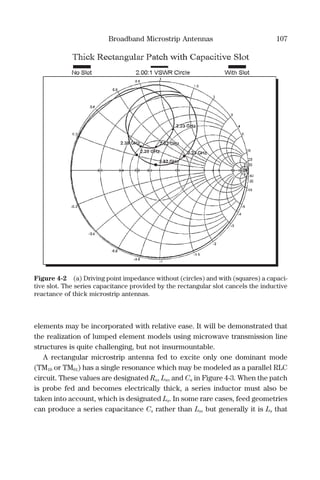


![110 Broadband Microstrip Antennas
We have now computed Ra, La, Ca, and Ls (or Cs in some rare cases). The
similarity of the model to a bandpass filter allows one to use filter synthesis
techniques to evaluate optimal component values for broadband matching.
This method was first articulated by Paschen.[10]
Optimum values may be found
in the literature.[11]
With a requirement of 1.8:1 VSWR (0.35 dB insertion loss)
the gi values for an N = 2 bandpass filter network are
g1 1 50= .
g2 0 455= .
g3 1 85= .
The component values of the bandpass filter are given by
C
g
RL U L
1
1
=
−( )ω ω
(4.18)
where ωU is the upper radian frequency band limit and ωL is the lower radian
frequency band limit. The filter bandwidth is
Fbw = ωU − ωL.
L
C
1
0
2
1
1
=
ω
(4.19)
L
g RL
U L
2
2
=
−( )ω ω
(4.20)
C
L
2
0
2
2
1
=
ω
(4.21)
Rin = RL/g3 (4.22)
We desire a 50 Ω input resistance, which requires that the load resistance
RL = g3 · 50 Ω = 92.5 Ω for this case. We now have all the equations required to
compute a matching example.](https://image.slidesharecdn.com/1891121731microstrip-151111163821-lva1-app6892/85/1891121731-microstrip-118-320.jpg)
![Broadband Microstrip Antennas 111
We need to provide Ra = 92.5 Ω, which is then equated with RL of the filter
circuit. We will do this by using a patch fed in the center of a radiating edge
with a microstrip transmission line. The patch width is adjusted to provide a
92.5 Ω edge resistance at resonance. We can compute the value of Ls from
measured or simulated data using the inductive reactance value XL:
L
X
s
L
=
ω0
(4.23)
When the inductive reactance is subtracted from two frequencies on either
side of resonance, we use equation (4.16) and equation (4.17) to compute Ca
and La. The value of Ca is equated with C1, which allows one to determine the
expected filter bandwidth Fbw using equation (4.18):
F
g
R Ca a
bw = 1
(4.24)
This computation can be used to decide if the bandwidth is acceptable for
a given design requirement. If the bandwidth is within the design requirement,
we next compute L2 using equation (4.20). This value needs to be larger than
the series inductance of the microstrip antenna Ls to realize the design. The
series inductance consists of two components, Lm and Lp. which are the series
inductance attributable to higher order modes and feed probe self-inductance,
respectively. While the majority of the series inductance Ls is due to the excita-
tion of higher order modes, a coaxial probe feed also contributes its self-induc-
tance Lp to the total series inductance. In some cases the diameter of this probe
may be used to adjust the series inductance to conform to a realizable design.[12]
Next, the value of C2 is computed from equation (4.21).
4.2.3 Example Microstrip Antenna Broadband Matching with
Lumped Elements
A microstrip antenna was designed, analyzed, and refined using FDTD to
create an element fed at a radiating edge with a 50 Ω microstrip transmission
line that has a 94.16 Ω impedance at resonance. This resistance is close
enough to realize an impedance matching design as detailed previously. The](https://image.slidesharecdn.com/1891121731microstrip-151111163821-lva1-app6892/85/1891121731-microstrip-119-320.jpg)
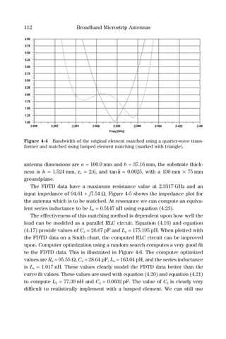


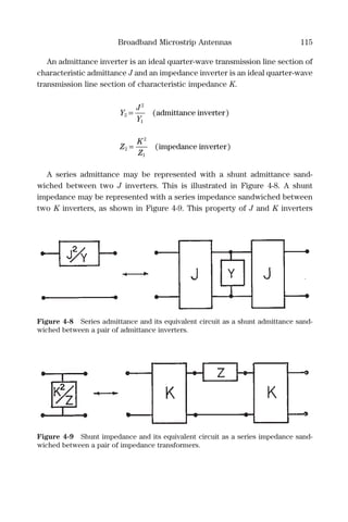


![Broadband Microstrip Antennas 119
4.2.5 Real Frequency Technique Broadband Matching
Another powerful matching method is the real frequency technique. Carlin
realized and demonstrated that traditional broadband matching methods
involving Chebyshev functions are optimum for purely resistive loads, but are
not optimum for complex loads.[13]
Carlin and Yarman introduced an alternate
version known as the simplified real frequency technique (SRFT), which they
demonstrated to be a very powerful method for the matching of microwave
circuits.[14]
The SRFT is much more flexible than using bandpass filter theory as a
matching method. With filter theory, one must choose the value of the resis-
tance in the RLC circuit based on achieving a 50 Ω input. The SRFT has the
flexibility that it can match any complex load whether it is a theoretical or
measured load impedance. Implementation of the SRFT is very involved.[15]
It
produces lumped element networks which are very effective, but conversion
to a transmission line realization remains very difficult. The SRFT has been
used to match microstrip antennas by Hongming et al.[16]
4.2.6 Matching Network Optimization Using Genetic Algorithms
When computer optimization is chosen as a method to develop a broadband
impedance matching network for a microstrip antenna, the choice of driving
point impedance of the patch antenna can be arbitrary. A popular contempo-
rary optimization method is the use of genetic algorithms.[17]
This optimization
method has the advantage that it is not difficult to implement and is conceptu-
ally accessible to the average designer. In an analogy with evolution, the limits
of the parameters to be optimized are coded into binary “genes” and concate-
nated to form “chromosomes.” A population of chromosomes is created with
the bits (ones and zeros) chosen by a random number generator. Generally a
random number generator produces numbers between zero and one. If the
value is below 0.5, the bit is set to zero, if it is greater than or equal to 0.5, the
bit is set to one. Each of the members of this initial population is evaluated
and assigned a normalized fitness value. The chromosomes are sorted and
ranked. An arbitrary percentage of chromosomes with the highest values of
fitness are retained. The chromosome with the highest fitness is “mated” with](https://image.slidesharecdn.com/1891121731microstrip-151111163821-lva1-app6892/85/1891121731-microstrip-127-320.jpg)

![Broadband Microstrip Antennas 121
• What microstrip patch shape provides maximum impedance bandwidth with
maximum linear polarization bandwidth allowing the linear polarization to
vary in direction over the bandwidth?
• What microstrip patch shape provides maximum impedance bandwidth with
maximum linear polarization bandwidth without rotation?
• What microstrip patch shape provides maximum impedance bandwidth with
maximum axial ratio bandwidth for a circularly polarized antenna.
One restriction on shape is to have a single continuous patch without
apertures (holes). One can relax this restriction and apply the same questions
previously stated.
4.3.1 Patch Shape Bandwidth Optimization Using Genetic
Algorithms
Delabie et al. proposed sectioning a plane in which a microstrip patch antenna
is to be created into a set of small square subpatches.[18]
Each subpatch is
metalized if represented by a one and no metal is present if represented by a
Figure 4-12 VSWR versus frequency using a genetic algorithm (marked with triangle)
and using a random search method to produce a matching network for the example
microstrip antenna. The quarter-wave sections were kept constant and only the length
of the transmission line stubs were varied in both cases.](https://image.slidesharecdn.com/1891121731microstrip-151111163821-lva1-app6892/85/1891121731-microstrip-129-320.jpg)
![122 Broadband Microstrip Antennas
zero. A set of chromosome representations of candidate patches are selected,
mated, and mutated using appropriate electromagnetic analysis technique.
The use of genetic algorithms to develop shapes which have increased
impedance bandwidths compared with a square microstrip patch has been
investigated by Choo et al.[19]
Each antenna is described by a grid of connected
squares with no internal voids. The patch antennas they developed use 1.6 mm
thick FR-4 substrate. Their groundplane size is 72 mm × 72 mm. Two cases
were examined, one using a 16 × 16 grid of squares; the second is a 32 × 32
grid of squares. The latter case is shown in Figure 4-13.
This patch is reported to have a fourfold increase in bandwidth improve-
ment when compared with a square microstrip antenna. This increase in band-
width is very close to the fundamental limit of increased bandwidth factor
(Section 4.1) when a matching network is implemented (Section 4.2).
32 × 32
72mm
Figure 4-13 Patch shape produced by a genetic algorithm using a 32 × 32 grid of
squares on a 72 mm × 72 mm groundplane. The substrate is 1.6 mm thick FR-4. (From
[19], copyright 2000, IEE. Reprinted with permission.)](https://image.slidesharecdn.com/1891121731microstrip-151111163821-lva1-app6892/85/1891121731-microstrip-130-320.jpg)
![Broadband Microstrip Antennas 123
The center frequency of the design bandwidth is 2.0 GHz. Simulation by the
method of moments predicted 8.04% bandwidth, and 8.10% was measured as
seen in Figure 4-14.
An FDTD analysis reveals this antenna combines two separate resonances
and creates circular polarization (LHCP) at 2.0 GHz. It is interesting to note
the genetic algorithm selected circular polarization. It was related in
Chapter 2, Section 2.7, that the impedance bandwidth of a patch with circular
polarization is two times that of a linear antenna. The patch shaping and
area apparently contribute to produce a further doubling of the impedance
bandwidth.
References
[1] Kumar, G., and Ray, K. P., Broadband Microstrip Antennas, London: Artech
House, 2003.
[2] Wong, K.-L., Compact and Broadband Microstrip Antennas, New York: John
Wiley & Sons, 2002.
–5
CH1 A/R log MAG 2.5 dB/ REF 0 dB 3; –10.374 dB
START 1 900 . 000 000 MHz STOP 2 200 . 000 000 MHz
2 039.950 002 MHz
–10
–15
–20
S11(dB)
1; –10.057 dB
2; –9.7897 dB
2.123 GHz
2
1.957 GHz
1
3
Figure 4-14 S11 versus frequency of the patch in Figure 4-13. (From [19], copyright
2000, IEE. Reprinted with permission.)](https://image.slidesharecdn.com/1891121731microstrip-151111163821-lva1-app6892/85/1891121731-microstrip-131-320.jpg)
![124 Broadband Microstrip Antennas
[3] Zurcher, J.-F., and Gardiol, F. E., Broadband Patch Antennas, London: Artech
House, 1995.
[4] Zurcher, J.-F., “The SSFIP: a global concept for high-performance broadband
planar antennas,” Electronics Letters, November 10, 1988, Vol. 24, No. 23, pp.
1433–1435.
[5] Zurcher, B., Zurcher, J.-F., and Gardiol, F. E., “Broadband microstrip radiators: the
SSFIP concept,” Electromagnetics, November 1989, Vol. 9, No. 4, pp. 385–393.
[6] Milligan, T., Modern Antenna Design, New York: McGraw-Hill, 1985, p. 104.
[7] Hall, P. S., “Probe compensation in thick microstrip patch antennas,” Electronics
Letters, May 21, 1987, Vol. 23, No. 11, pp. 606–607.
[8] Bernard, R., Tchanguiz, R., and Papiernik, A., “Capacitors provide input matching
of microstrip antennas,” Microwaves & RF, July 1994, Vol. 33, No. 7, pp.
103–106.
[9] Matthaei, G., Young, L., and Jones, E. M. T., Microwave Filters, Impedance-Match-
ing Networks, and Coupling Structures, New York: McGraw Hill, 1964, pp. 120–
130, 681–686.
[10] Paschen, D. A., “Practical examples of integral broadband matching of microstrip
elements,” Proceedings of the 1986 Antenna Applications Symposium, Monticello,
Illinois, September 17–19, 1986, pp. 199–217.
[11] Matthaei, G. L., Young, L., and Jones, G. M. T., Microwave Filters, Impedance-
Matching Networks, and Coupling Structures, New York: McGraw Hill, 1964, pp.
123–129.
[12] Schaubert, D. H., Pozar, D. M., and Adrian, A., “Effect of microstrip antenna sub-
strate thickness and permittivity: comparison of theories with experiment,” IEEE
Transactions on Antennas and Propagation, June 1989, Vol. 37, No. 6, pp.
677–682.
[13] Carlin, H. J., and Amstutz, P., “On optimum broad-band matching,” IEEE
Transactions of Circuits and Systems, May 1981, Vol. CAS-28, No. 5, pp.
401–405.
[14] Yarman, B. S., “A simplified real frequency technique for broadband matching a
complex generator to a complex load,” RCA Review, September 1982, Vol. 43, pp.
529–541.
[15] Gerkis, A. N., “Broadband impedance matching using the ‘real frequency’ network
synthesis technique,” Applied Microwave & Wireless, July/August 1998, pp.
26–36.
[16] Hongming, A., Nauwelaers, B. K. J. C., and Van de Capelle, A. R., “Broadband
microstrip antenna design with the simplified real frequency technique,” IEEE
Transactions on Antennas and Propagation, February 1994, Vol. 42, No. 2, pp.
129–136.](https://image.slidesharecdn.com/1891121731microstrip-151111163821-lva1-app6892/85/1891121731-microstrip-132-320.jpg)
![Broadband Microstrip Antennas 125
[17] Rahmat-Samii, Y., and Michielssen, E., eds., Electromagnetic Optimization by
Genetic Algorithms, New York: John Wiley & Sons, 1999.
[18] Delabie, C., Villegas, M., and Picon, O., “Creation of new shapes for resonant
microstrip structures by means of genetic algorithms,” Electronics Letters, August
28, 1997, Vol. 33, No. 18, pp. 1509–1510.
[19] Choo, H., Hutani, A., Trintinalia, L. C., and Ling, H., “Shape optimization of broad-
band microstrip antennas using genetic algorithm,” Electronics Letters, December
7, 2000, Vol. 36, No. 25, pp. 2057–2058.](https://image.slidesharecdn.com/1891121731microstrip-151111163821-lva1-app6892/85/1891121731-microstrip-133-320.jpg)
![Chapter 5
Dual-Band Microstrip Antennas
5.0 Dual-Band Microstrip Antennas
Dual-band microstrip antennas are generally of two types: 1) separate microstrip
resonators coupled to a transmission line, or 2) perturbed microstrip resona-
tors where their original resonant frequencies are shifted by geometrical
alteration of a basic resonator.[1,2]
Dual-band microstrip antenna designs
which allow for independent frequency selection have the most design utility.
A good overview of dual-band microstrip antennas is given by Maci and
Gentili.[3]
5.1 Single-Resonator Rectangular Microstrip Dual-Band Antenna
If one requires a single element, dual-band microstrip antenna that has a
broadside radiation pattern at each of the dual-band design frequencies with
the same polarization, one must drive the TM10 and TM30 modes. When these
restrictions are chosen, the upper frequency must be approximately three
times the lower frequency of operation. For a rectangular microstrip antenna,
the pattern and polarization restrictions which have been previously imposed,
severely limit the number of applications for which this design may be
utilized.
In Section 2.6.1, a rectangular microstrip antenna is used to create circular
polarization by allowing the TM10 and TM01 modes to overlap in frequency. A
similar approach can be used to create a single resonator (element), dual-band
microstrip antenna by separating the modes until they are isolated. If a designer
can allow orthogonal linear polarization for each of the dual-band frequencies,
and desires broadside radiation patterns, one can choose rectangular patch
126](https://image.slidesharecdn.com/1891121731microstrip-151111163821-lva1-app6892/85/1891121731-microstrip-134-320.jpg)
![Dual-Band Microstrip Antennas 127
dimensions a and b so the TM10 and TM01 modes correspond to a desired upper
and lower frequency pair (FU, FL). This allows one to choose the two frequen-
cies of operation in an independent fashion. One can choose the patch dimen-
sions a and b to produce the desired frequency pair using methods from
Chapter 2. The feed point location (Xp, Yp) is the place which will optimally
match the two modes simultaneously. The transmission line model of a rect-
angular microstrip antenna allows one to feed a patch antenna anywhere along
a plane that is 50 Ω. A 50 Ω driving point impedance plane exists for each of
the two modes generated. Where the impedance planes intersect is an optimum
point to feed a dual-band patch of this type.[4]
The geometry of a dual-band
patch antenna of this type is illustrated in Figure 5-1.
In order to avoid the inaccuracies that can occur using the transmission line
model, one can use the cavity model with genetic optimization to design a
dual-band patch based on the use of TM01 and TM10. This approach allows us
to study the feasibility of designs using different frequency separations.
For ease of analysis, we can define a midpoint frequency Fm which is cen-
tered between the dual-band frequencies FL and FU:
F
F F
m
L U
=
+
2
We can define a frequency separation factor:
F
F
F
s
m F
m F
=
+
−
∆
∆
with
∆F
U L
m
s
s
F F
F
F
F
=
−
=
−
+2
1
1
( )
( )
Multiplying the lower frequency by this factor produces the upper frequency:
F F F FU s L m F= ⋅ = + ∆](https://image.slidesharecdn.com/1891121731microstrip-151111163821-lva1-app6892/85/1891121731-microstrip-135-320.jpg)

![Dual-Band Microstrip Antennas 129
Fit L U
L U
L U= ⋅ − + −
Min
Max
( , )
( , )
[( ) ( )]
Γ Γ
Γ Γ
Γ Γ1 1
where
|ΓL| = magnitude of the driving point reflection coefficient at the lower center
frequency
|ΓU| = magnitude of the driving point reflection coefficient at the upper center
frequency.
We note in Figure 5-2 that as the frequency separation becomes larger, the
genetic algorithm produces designs that are very close to the desired design
frequencies and well matched (>20 dB return loss). An Fs of 1.05 is a design in
which genetic optimization is unable to match both frequencies. When Fs > 1.2,
genetic optimization produces well-matched dual-band designs for the rectan-
gular patch geometry.
Figure 5-2 Single-feed dual-band solutions for a rectangular microstrip antenna using
a genetic algorithm optimization with the cavity model.](https://image.slidesharecdn.com/1891121731microstrip-151111163821-lva1-app6892/85/1891121731-microstrip-137-320.jpg)
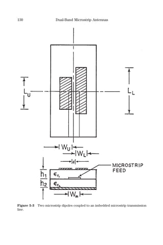

![132 Dual-Band Microstrip Antennas
feed probe connects to the lower patch, and the upper patch is electromagneti-
cally coupled. Parasitic feeding is often used to broaden the bandwidth of the
upper patch rather than produce a dual-band antenna. When used to broaden
antenna bandwidth, the upper patch is larger than the lower patch.[5]
When the upper patch is directly fed, the feed point location for a set of
stacked linear rectangular microstrip antennas is close to the location of each
patch separately. A shorting pin can be placed through the center of both
Figure 5-4 Microstrip dipole dual-band designs of Table 5-1 analyzed with FDTD.
Table 5-1 Coupled dual-band microstrip antenna parameters.
Fs LL (mm) LU (mm) WL (mm) WU (mm)
2.15 31.20 13.52 9.50 6.20
1.60 25.73 15.00 9.50 6.20
1.25 21.78 16.83 9.50 6.20
εr1
= εr2
= 4.1 tanδ = 0.005 h1 = h2 = 1.524 mm d = 2 mm
Microstrip Line Width = 2.98 mm](https://image.slidesharecdn.com/1891121731microstrip-151111163821-lva1-app6892/85/1891121731-microstrip-140-320.jpg)

![134 Dual-Band Microstrip Antennas
element configurations with a smaller footprint than required by half-wave
elements.
As stated previously, the upper and lower patches may have their aspect
ratios adjusted so the upper and lower patches can have their TM01 and TM10
modes driven at distinct frequencies. This allows one to create a pair of stacked
patches that will operate at four separate frequencies.
One can create a quad-band stacked patch antenna using the cavity model
with genetic algorithms, as detailed in Section 5.1. A dual-band patch design,
as shown in Figure 5-1, is the starting point. The two lowest frequencies are
assigned to the bottom patch antenna and the two highest frequencies are
assigned to the upper rectangular patch antenna. Lengths aL and bL are chosen
to resonate the TM10 and TM01 of the lower patch at the desired lower set of
design frequencies. Lengths aH and bH are chosen to resonate the TM10 and TM01
of the upper patch at the desired high set of design frequencies.
A pair of 50 Ω impedance planes, as shown in Figure 5-1, will exist for
each of the two antennas. The point of intersection of the impedance
planes of the upper patch antenna (XPU,YPU) is aligned with the lower patch’s
intersection point (XPL,YPL). The two points are colocated as (XP,YP) in
Figure 5-6. Experimental optimizing of the antenna is required to produce a
final design.
5.3 Dual-Band Microstrip Antenna Design Using a Diplexer
An alternative to using a stacked patch to create a dual-band microstrip antenna
is to use a diplexer with two single-frequency elements. A diplexer separates
a pair of frequency bands that are originally combined at the input port and
presents each frequency at each of a pair of output ports which are isolated
from one another. The classic lumped element version of a diplexer consists
of a high-pass filter and low-pass filter with a common input.
The exact and approximate design of diplexers and multiplexers is pre-
sented in the literature.[6,7]
This design process can be rather extensive when
developing microwave diplexers. If the frequency ratio between bands is
approximately 2:1, one can use a diplexer circuit, introduced by de Haaij et
al. and presented in Figure 5-7.[8]](https://image.slidesharecdn.com/1891121731microstrip-151111163821-lva1-app6892/85/1891121731-microstrip-142-320.jpg)


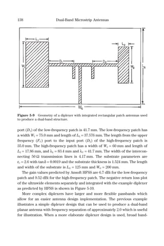

![140 Dual-Band Microstrip Antennas
width planar antenna element designs allow one to develop designs with up
to 20% bandwidth per band by using planar antennas (i.e., monopole-type
elements).
5.4 Multiband Microstrip Design Using Patch Shaping and a Genetic
Algorithm
In Section 4.3, the creation of microstrip antennas with a large impedance
bandwidth using patch shaping guided with a genetic algorithm was discussed.
This method has been used by Choo and Ling to design a microstrip antenna
patch shape using the method of moments, which produces multiband anten-
nas on FR-4.[9,10]
An antenna shape was created which operates at 900 MHz
(GSM), 1.6 GHz (GPS/L1), 1.8 GHz (DCS), and 2.45 GHz (ISM/Bluetooth).
This design is reproduced in Figure 5-11. This method offers the possibility
–5
Cor
CH1 A/R log MAG 2.5 dB/ REF 0 dB 4; –14.29 dB
144mm
0.80 1.16 1.52 1.88 2.24 2.60
Frequency (GHz)
897.510 MHz
0.004 MHz
–10
–15
–20
S11(dB)
2; –9.4059 dB
1; –18.944 dB
3; –22.270 dB
1.608 GHz
1.611 GHz
Figure 5-11 Patch shape of a microstrip antenna that has been optimized for quad-
band operation. The dashed lines are simulation and the solid line is measurement.
(From [9], copyright 2002, IEEE. Reprinted with permission.)](https://image.slidesharecdn.com/1891121731microstrip-151111163821-lva1-app6892/85/1891121731-microstrip-148-320.jpg)
![Dual-Band Microstrip Antennas 141
of developing low-cost single-layer multiband antennas with arbitrary
frequencies.
References
[1] Kumar, G., and Ray, K. P., Broadband Microstrip Antennas, London: Artech
House, 2003.
[2] Wong, K.-L., Compact and Broadband Microstrip Antennas, New York: John
Wiley & Sons, 2002.
[3] Maci, S., and Gentili, G. B., “Dual-frequency patch antennas,” IEEE Antennas and
Propagation Magazine, December 1997, Vol. 39, No. 6, pp. 13–20.
[4] Chen, J.-S., and Wong, K.-L., “A single-layer dual-frequency rectangular microstrip
patch antenna using a single probe feed,” Microwave and Optical Technology
Letters, February 5, 1996, Vol. 11, No. 2, pp. 83–84.
[5] James, J. R., and Hall, P. S., Handbook of Microstrip Antennas, Vol. 1, Stevenage,
UK: Peter Peregrinus, Ltd., 1989, pp. 324–325.
[6] White, J. F., High Frequency Techniques, New York: John Wiley & Sons, 2004,
pp. 364–369.
[7] Malherbe, J. A. G., Microwave Transmission Line Filters, London: Artech House,
1979, chap. 7.
[8] de Haaij, D. M., Joubert, J., and Odendaal, J. W., “Diplexing feed network for
wideband dual-frequency stacked microstrip patch antenna,” Microwave and
Optical Technology Letters, January 20, 2003, Vol. 36, No. 2, pp. 100–103.
[9] Choo, H., and Ling, H., “Design of multiband microstrip antennas using a genetic
algorithm,” IEEE Microwave and Wireless Components Letters, September 2002,
Vol. 12, No. 9, pp. 345–347.
[10] Choo, H., and Ling, H., “Design of dual-band microstrip antennas using the genetic
algorithm,” Proceedings of the 17th Annual Review of Progress in Applied
Computational Electromagnetics, Session 15, Monterey, CA, May 19–23, 2001,
pp. 600–605.](https://image.slidesharecdn.com/1891121731microstrip-151111163821-lva1-app6892/85/1891121731-microstrip-149-320.jpg)
![Chapter 6
Microstrip Arrays
6.0 Microstrip Arrays
A single microstrip antenna utilizing an air dielectric substrate (εr ≈ 1) is able
to provide a maximum gain of about 10 dBi. When larger gains are required,
and a microstrip antenna solution is the best choice, a number of microstrip
elements may be connected together to form an array of antennas. An array of
elements provides a much larger effective aperture and therefore gain com-
pared to a single microstrip element. This chapter will discuss elementary
methods used to design microstrip antenna arrays.
6.1 Planar Array Theory
Classic linear and planar array analysis papers were presented by Elliot in
the early 1960s which are very useful for the analysis of rectangular microstrip
antenna arrays.[1–3]
In Figure 6-1, a number of rectangular microstrip antennas
are located in the x-y plane. The z axis is directed out from the paper.
Each microstrip antenna can be modeled as a pair of radiating slots in a
groundplane. Assuming a TM01 mode, the antennas are polarized along the y
axis. A patch with its center located at (Xn,Yn) is effectively modeled as
a pair of slots located at (Xn,Yn + L/2) and (Xn,Yn − L/2) of width W and
thickness H and identical excitation amplitude for each pair as shown in
Figure 6-2.
The array factor for a number of point sources (Np) in free space is
A I en
jk X Y
n
N
n n
p
( , ) sin [ cos sin ]
θ φ θ φ φ
= +
=
∑
1
(6.1)
142](https://image.slidesharecdn.com/1891121731microstrip-151111163821-lva1-app6892/85/1891121731-microstrip-150-320.jpg)
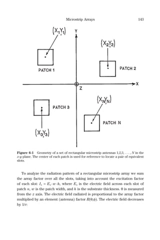
![144 Microstrip Arrays
E A R( , ) ( , ) ( , )θ φ θ φ θ φ= ⋅ (6.2)
The θ and φ components of the electric field are
E A Rθ θ φ θ φ φ θ φ( , ) ( , )sin ( , )= ⋅ (6.3)
E A Rφ θ φ θ φ θ φ θ φ( , ) ( , )cos cos ( , )= ⋅ (6.4)
The element factor for a rectangular aperture is[4]
Y
L
W
Φ
h
(Xn,Yn)
(Xn,Yn + –)
2
L
(Xn,Yn – –)
2
L
XZ
Figure 6-2 The radiation from each patch of Figure 6-1 is modeled as a pair of
slots.](https://image.slidesharecdn.com/1891121731microstrip-151111163821-lva1-app6892/85/1891121731-microstrip-152-320.jpg)
![Microstrip Arrays 145
R
kw u
kw u
kh v
kh v
( , )
sin[( / ) ]
( / )
sin[( / ) ]
( / )
θ φ =
2
2
2
2
(6.5)
where
u = sin cosθ φ (6.6)
v = sin cosθ φ (6.7)
The power at any point in space is
P r
E
r
E
r
( , , )θ φ θ φ
= +
2
2
2
2
(6.8)
We can multiply equation (6.8) by r2
, which gives us the power per unit solid
angle or the radiation intensity U:
U E E( , )θ φ θ φ= +
2 2
(6.9)
The expression for radiation intensity can be used to compute the array
directivity using numerical techniques:[5]
D
U
Prad
0
4
=
π max
(6.10)
P
N M
Urad i j i
i
N
j
M
=
==
∑∑
π π
θ φ θ
2
11
( , )sin (6.11)
where
θ
π
i i
N
=
(6.12)
θ
π
j j
M
=
2
(6.13)](https://image.slidesharecdn.com/1891121731microstrip-151111163821-lva1-app6892/85/1891121731-microstrip-153-320.jpg)


![150 Microstrip Arrays
and the minimized gain of a binomial array with −∞ dB sidelobes is an optimum
choice known as a Dolph-Chebyshev distribution.[6]
The realization of a Dolph-
Chebyshev distribution, however, can prove to be very challenging. Often, in
practice, nonoptimum aperture distributions relinquish only a small amount of
gain and are more readily realizable than an optimum distribution. A normal-
ized linear taper on a pedestal is one which has a maximum value of one at the
center of the array and tapers to a value of C at the maximum extent of the
array. Because the distribution tapers to a nonzero value at its edge, it is said to
be on a pedestal. A cosine on a pedestal distribution superimposes a cosine
curve which has a nonzero value of C at the edges of an array. The expressions
that describe these distributions are summarized below:
• Uniform
In = 1 (6.14)
• Linear taper on a pedestal
I C C
x
L
n
n
A
= + − −
( )1 1 (6.15)
• Cosine taper on a pedestal
I C C
x
L
n
n
A
= + −
( )cos1
2
π
(6.16)
• Cosine squared taper on a pedestal
I C C
x
L
n
n
A
= + −
( )cos1
2
2 π
(6.17)
• Quadratic taper on a pedestal
I C C
x
L
n
n
A
= + − −
( )1 1
2
(6.18)](https://image.slidesharecdn.com/1891121731microstrip-151111163821-lva1-app6892/85/1891121731-microstrip-158-320.jpg)
![Microstrip Arrays 151
xn is the location of the nth element along the x axis, as shown in Figure 6-6
for a linear taper. The length of the array is 2LA. In is the excitation value for
each element n. For an array with an odd number of elements, the element at
the center of the array is located at x0 and has a normalized value equal to one
(I0 = 1). When an array has an even number of elements, the I0 element is
removed and only the even elements remain. Figure 6-6 illustrates a linear taper
on a pedestal of value C. The excitation distribution is linear in Figure 6-6 and
is on a pedestal of value C. The value of C may be expressed as a decibel level
with respect to the unity excitation value in the center:
C CdB
= 10 20 0( / . )
(6.19)
For a −16 dB taper we compute C = 0.1585, which may be used in equations
(6.15) through (6.18). Figure 6-5 contains patterns computed with a uniform,
linear, and cosine taper computed with equation (6.15) and equation (6.16) and
using the values of the 5.3 GHz patches in the previous section. We can see
that for a 64-element, 8 × 8 array, the uniform distribution provides the maximum
main beam gain of 23.60 dBi (assuming 100% efficiency). We can reduce the
sidelobe level to −21.7 dB with a −16 dB linear taper, and the gain of the main
beam decreases by 0.70 dB, which is the trade-off one makes for a lower side-
lobe level. A −16 dB cosine squared on a pedestal reduces the main beam gain
by −1.20 dB compared with a uniform distribution, but the sidelobe level is
now approximately −26 dB. Figure 6-6 presents an illustration of how the aper-
ture functions are sampled to determine the excitation values, In. The origin
of the coordinate system is on the center of patch 1. A vector to the center-most
patch is formed. For an even array—2 × 2, 4 × 4, etc.—rc is a vector to the
center of the array. In the geometry of Figure 6-7, equation (6.20) describes the
location of rc. The vector from each patch to the array center patch, rd [equa-
tion (6.21)], is used to provide the distance dn(= xn) [equation (6.22)]. The value
LA is defined with equation (6.23). The values of dn and LA are placed into equa-
tion (6.15) for a linear taper on a pedestal and equation (6.16) for a cosine taper
on a pedestal for each n patch element.
r
L
i
L
jc
x y
= +
2 2
ˆ ˆ (6.20)](https://image.slidesharecdn.com/1891121731microstrip-151111163821-lva1-app6892/85/1891121731-microstrip-159-320.jpg)
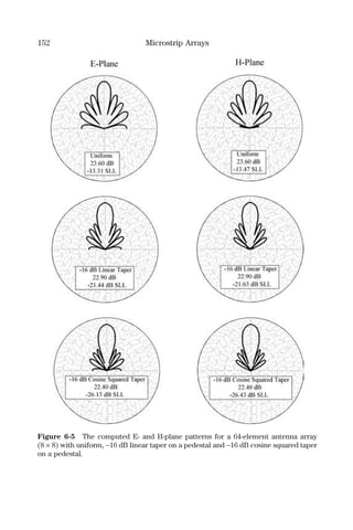


![Microstrip Arrays 155
amplitude taper can prove to be difficult. The design details of series fed arrays
will be addressed in the next section.[7]
To illustrate an elementary corporate feed network we will feed a linear
array of four patch antennas, as illustrated in Figure 6-8. Each of the identical
square patch antennas has an element input resistance Rin at resonance [Rin =
Re/2 = 1/(2Ge)]. This element resistance at each patch may be matched to
connecting transmission line impedances Z1, Z2, Z3, Z4, which will be used to
provide a desired power split. This is accomplished with a number of quarter-
wave transformers: Zq
1
, Zq
2
, Zq
3
, Zq
4
.
To simplify this design we will feed the linear array with a 50 Ω microstrip
transmission line into a pair of 100 Ω lines. This will split the power in an equal
manner to Za and Zb quarter-wave transformers. These transformers are used
to match between the 100 Ω feed line and the pair of transmission lines used
to divide the incident power between each pair of patches (i.e., 1 and 2, 3 and
4). In the case of patch 1 and patch 2, we wish to provide them with current
Figure 6-8 Four patch linear array fed with a microstrip corporate feed network.](https://image.slidesharecdn.com/1891121731microstrip-151111163821-lva1-app6892/85/1891121731-microstrip-163-320.jpg)

![Microstrip Arrays 157
Z Z Rq in
2
2 53 11 271 21 120 02= ⋅ = ⋅ =. . . .Ω
The impedance at the power split is Z1||Z2 = 36.77 Ω. The quarter-wave trans-
former Za is found as 36 77 100 0. .⋅ = 60.64 Ω.
In this case we have chosen a symmetric array distribution so the values of
the impedances for both sides have been evaluated. The loss in a corporate
fed array will increase as substrate height increases and dielectric constant
decreases. The loss also increases as the feed line impedances decrease.[8]
As
the dimensions of an array increase, the length of the corporate feed network
extends further and further. The microstrip line losses increase and decrease
the realized gain of the array and also add to the antenna noise figure. One can
reach a point of diminishing return. As the number of array elements (and thus
the effective aperture) are increased, the losses from the feed network become
larger and larger. The increase in gain produced by a larger aperture can be
balanced by the losses in the feed lines or overtaken.
This method of creating a feed network can be used to design the feed
network of a planar array. Figure 6-9 has a 4 × 4 (16 elements) planar array fed
with a corporate network. This antenna can be sectioned into four 2 × 2 sub-
arrays. The distribution can be computed for a subarray and the subarrays can
be arrayed to create a planar array.
6.4.2 Series Fed Microstrip Array
A set of microstrip patches may be fed in series with microstrip transmission
line connecting their radiating edges.[9,10]
This is illustrated in Figure 6-10(a).
The microstrip realization of the series array is on the left in Figure 6-10. The
patches are separated by microstrip transmission line which has a λ/2 guide
wavelength. In theory the characteristic impedance of the transmission line is
not critical because each of the loads created by the edges of a microstrip
radiator are all one-half wavelength in spacing. This is shown in the illustration
of Figure 6-10(b). At resonance, the pair of slots of each rectangular microstrip
element may be combined to form an equivalent admittance. A load that rep-
resents each patch is separated by half-wavelength sections of microstrip
transmission line. This is illustrated in Figure 6-10(c). This separation allows
one to compute the input resistance of the series fed array at resonance as](https://image.slidesharecdn.com/1891121731microstrip-151111163821-lva1-app6892/85/1891121731-microstrip-165-320.jpg)
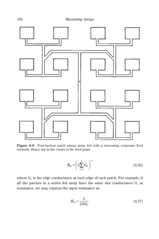

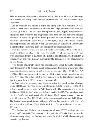
![Microstrip Arrays 161
The main beam of a series array is broadside to the array at resonance with
proper spacing. The main beam will squint from broadside with frequency. The
bandwidth of this type of array is rather narrow and in general only about 1 %
to 2%.[11]
As additional patches are added, the impedance bandwidth of a series
array narrows.
The previous design example has patches of identical width. When this is
the case, all the elements have the same excitation amplitude.
If we wish to produce an amplitude taper to decrease the array sidelobe
level we can change the widths of each patch to accept a designated amount
of power. The power accepted by the nth element of a series array is
P g Vn n= 2 2
(6.28)
The value gn is the conductance of each antenna n normalized to the desired
driving point resistance, which in this case is 50 Ω:
Figure 6-11 Four-by-four patch with uniform element excitation planar array.](https://image.slidesharecdn.com/1891121731microstrip-151111163821-lva1-app6892/85/1891121731-microstrip-169-320.jpg)

![Microstrip Arrays 163
Gn = constant). A realistic taper for the physical realization of a four-element
series array is to widen the two center elements by a factor of 1.5 and reduce
the outer elements to one-half of the original width. When this is done, the sum
of the conductances remains constant and the series array remains matched
as it was in the uniform conductance example. FDTD analysis results demon-
strate the input match and the resonant frequency of 5.09 GHz remain constant
when the array is modified in this way. The modified array is shown in
Figure 6-12. This tapering of the patch widths translates to a −4.04 dB linear
taper. The array directivity is 12.86 dB.
The pattern computed by FDTD analysis is shown in Figure 6-13. We can
see the sidelobe on the left side at approximately 45˚ has all but vanished, and
the sidelobe on the right at approximately 30˚ has been reduced considerably.
If one chooses to widen the inner two patches further and narrow the outer
two patches so a 50 Ω driving point impedance is maintained, the narrow
patches will be more affected by the feed lines as their dimension decreases.
A second option for a series fed array is to feed the antennas along nonra-
diating edges. One can choose the position of each input and output location
on each patch to provide a desired amplitude taper. The design of this type
of array is very involved mathematically and details may be found in the
literature.[12–14]
6.5 Phase and Amplitude Error
The arrays examined in this chapter all assume the currents in the radiating
elements of an array are excited in phase (i.e., In∠0˚) with the proper ampli-
tudes. In any physically realized array, the phase of the excitation current of
the elements in the array will deviate from the desired phase values. The
sources of error are numerous. The dielectric constant and thickness of a
substrate material can vary with location in a given sheet. This changes the
propagation constant of the microstrip lines as well as their impedance values.
The driving point impedance of elements will be affected as well. When ele-
ments are closely located, mutual coupling can introduce amplitude and phase
error. A good introduction to the effects encountered because of mutual cou-
pling is given by Malherbe.[15]
Although corrections for microstrip discontinui-
ties are presented in Appendix C, their relative accuracy can produce phase](https://image.slidesharecdn.com/1891121731microstrip-151111163821-lva1-app6892/85/1891121731-microstrip-171-320.jpg)


![Microstrip Arrays 167
The N´ in equation (6.37) means the sum which excludes the m = n
term.
The currents at each of the elements is unknown initially, but we can use
equation (6.37) to iterate to a solution starting with an initial guess at the
driving point currents. The starting current for the array can be computed by
dividing the driving point voltages by each antenna’s self-impedance neglecting
coupling:
I
E
Z Z
n
s n
nn
1
0
=
+
(6.38)
We can then use equation (6.37) to calculate a new active impedance.
After the active impedance has been calculated, we calculate a new current
distribution, keeping the voltage distribution constant. The current at the kth
iteration is
I
E
Z Z
n
fk n
an
=
+ 0
(6.39)
The superscript f is the final current for iteration k and which drives
element n.
A new starting current for iteration k + 1 is found with
I I In
s k
n
sk
n
fk( )+
= +1 1
2
(6.40)
At each iteration an error is evaluated using
Error = − + −
=
∑ Re Re Im Im[ ] [ ] [ ] [ ]I I I Ii
fk
i
sk
i
fk
i
sk
i
N
2 2
1
(6.41)
The mutual coupling terms may be computed using the cavity model as
related in Section 6.6.1 After the currents have been calculated, the techniques
of sections 6.1, 6.2, and 6.3 are used to compute the radiation pattern of the
array.](https://image.slidesharecdn.com/1891121731microstrip-151111163821-lva1-app6892/85/1891121731-microstrip-175-320.jpg)

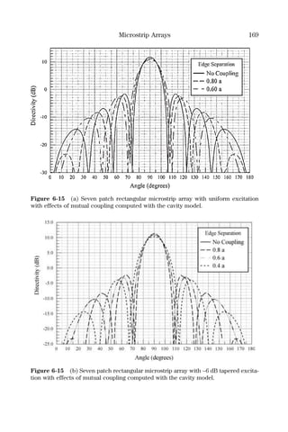
![170 Microstrip Arrays
an edge-to-edge separation of 0.8a we see that, as before, the directivity
decreases but the sidelobe level increases. At ∆ = 0.6a, the coupling is
such that the current distribution is almost identical to that without
mutual coupling. When the spacing is decreased to 0.4a, the directivity
decreases.
6.6.1 Mutual Coupling Between Square Microstrip Antennas
The mutual coupling between two microstrip antennas may be calculated using
the following relationship:[16]
Z
I I
H M dlpatch patch
21
1 2
1 2
2
1
= ∫ i (6.42)
One can use the cavity model with equation (6.42) to obtain the mutual imped-
ance between probe fed microstrip antennas. I1 and I2 are the currents at the
feeds of the patches. Hpatch1
is the magnetic field on antenna 2 produced by
antenna number 1. Mpatch2
is the linear magnetic current density on antenna 2
when it has been self-excited. The integration is over the perimeter of antenna
2. The dimensions for this analysis are defined in Figure 6-16.
The patches are located in the x-y plane. The center of patch 1 is the origin
of the coordinate system. The center of patch two is at r0 = X0iˆ + Y0 jˆ. We cal-
culate Hpatch1
from the magnetic current at the edge of patch 1. The equivalent
magnetic line currents at the edge of the cavity are related to the field at the
boundary of the cavity by
M HE x y z npatch
z
2
2= ×( , ) ˆ ˆ (6.43)
The unit vector nˆ is an outward normal at the cavity boundary and H is the
substrate thickness. The interior electric field is calculated using the cavity
model. This relationship is given by
E x y
jI
y
b
y
b
ab j
z
p
r i
( , )
cos cos
[ ( ) ]
=
− +
2 0
2 2
ω
π π
ε ω ω ω*
(6.44)](https://image.slidesharecdn.com/1891121731microstrip-151111163821-lva1-app6892/85/1891121731-microstrip-178-320.jpg)

![172 Microstrip Arrays
The magnetic field radiated by a small zˆ directed magnetic current M of
length ∆z is given by[17]
H r jw
M z
jkr jkr
e
r
j
M z
jkr
( , ) = + +
( )
sin +θ ε
π
θθ
ωε
∆
∆
4
1
1 1
2
2
−
ˆ
ππ
θ1
1
2
+
( )
cos
jkr
e
r
r
jkr
−
ˆ (6.45)
For a magnetic current of differential length dz, the differential magnetic
field simply becomes
dH r jw
Mdz
jkr jkr
e
r
j
Mdz
jkr
( , ) = + +
( )
sin +θ ε
π
θθ
ωε
4
1
1 1
2
−
ˆ
22
1
1
2
π
θ+
( )
cos
jkr
e
r
r
jkr
−
ˆ (6.46)
Figure 6-17 Direction of magnetic current on each side of a rectangular microstrip
patch antenna defined by equation (6.43) with the cavity model.](https://image.slidesharecdn.com/1891121731microstrip-151111163821-lva1-app6892/85/1891121731-microstrip-180-320.jpg)
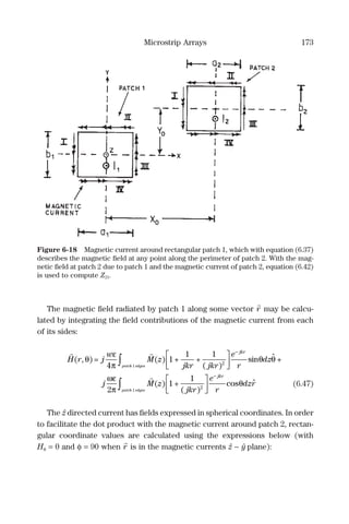

![Microstrip Arrays 175
− →H Hy
M
y
H Hz
M
x→
Now that we have calculated the magnetic field from the center of patch 1
at any given distance r, we may now dot it with the magnetic current around
the edge of patch 2 and integrate the resulting function. This completes the
evaluation of equation (6.42).
Figure 6-20 Comparison of experimental results of Jedlicka and Carver [16] with
those computed with equation (6.42) using the cavity model: f = 1.56 GHz, εr = 2.50,
a1 = a2 = 50.0 mm, b1 = b2 = 60.0 mm, H = 1.57 mm. The probe feed is located at
the center x = a/2 of each patch with the probe fed at 8.25 mm from the center
(Rin = 50.125 Ω).](https://image.slidesharecdn.com/1891121731microstrip-151111163821-lva1-app6892/85/1891121731-microstrip-183-320.jpg)
![176 Microstrip Arrays
The coupling between a pair of rectangular microstrip antennas has been
evaluated and compared with the experimental results of Jedlicka and Carver.[18]
The theoretical results are plotted with the experimental results of Jedlicka
and Carver in Figure 6-20. The correlation between experiment and theory is
good overall and very good from 0.3 to 0.6 λ edge separation.
References
[1] Elliot, R. S., “Bandwidth and directivity of large scanning arrays, first of two parts,”
Microwave Journal, December 1963, Vol. 6, No. 12, pp. 53–60.
[2] Elliot, R. S., “Beamwidth and directivity of large scanning arrays, last of two parts,”
Microwave Journal, January 1964, Vol. 7, No. 1, pp. 74–82.
[3] Hansen, R. C., Significant Phased Array Papers, London: Artech House, 1973.
[4] Stutzman, W. L., and Thiele, G. A., Antenna Theory and Design, John Wiley & Sons,
1981, pp. 385–391.
[5] Balanis, C. A., Antenna Theory Analysis and Design, New York: Harper & Row,
1982, pp. 37–42.
[6] Dolph, C. L., “A current distribution for broadside arrays which optimizes the
relationship between beamwidth and sidelobe level,” Proceedings IRE, June 1946,
Vol. 34, No. 6, pp. 335–348.
[7] Sainati, R. A., CAD of Microstrip Antennas for Wireless Applications, London:
Artech House, 1996, pp. 191–199.
[8] Hall, P. S., and Hall, C. M., “Coplanar corporate feed effects in microstrip
patch array design” IEE Proceedings, June 1988, Vol. 135, Pt. H, No. 3, pp.
180–186.
[9] Sainati, R. A., CAD of Microstrip Antennas for Wireless Applications, London:
Artech House, 1996, pp. 210–220.
[10] Collin, R. E., Antennas and Radiowave Propagation, New York: McGraw-Hill,
1985, pp. 266–268.
[11] Derneryd, A. G., “Linearly polarized microstrip antennas,” IEEE Transactions on
Antennas and Propagation, November 1976, Vol. 24, No. 6, pp. 846–851.
[12] Derneryd, A. G., “A two port rectangular microstrip antenna element,” Scientific
Report No. 90, Electromagnetics Laboratory, University of Colorado, Boulder, CO,
July 1987.
[13] Gupta, K. C., and Benalla, A., “Transmission-line model for two-port rectangular
microstrip patches with ports at the nonradiating edges,” Electronics Letters,
August 13, 1987, Vol. 23, No. 17, pp. 882–884.](https://image.slidesharecdn.com/1891121731microstrip-151111163821-lva1-app6892/85/1891121731-microstrip-184-320.jpg)
![Microstrip Arrays 177
[14] Gupta, K. C., and Benalla, A., “Two-port transmission characteristics of circular
microstrip patch antennas,” Antennas and Propagation Society International
Symposium, June 1986, Vol. 24, pp. 821–824.
[15] Malherbe, A., and Johannes, G., “Analysis of a linear antenna array including
the effects of mutual coupling,” IEEE Transactions on Education, February 1989,
Vol. 32, No. 1, pp. 29–34.
[16] Huynh, T., Lee, K. F., and Chebolu, S. R., “Mutual coupling between rectangular
microstrip patch antennas,” Microwave and Optical Technology Letters, October
1992, Vol. 5, No. 11, pp. 572–576.
[17] Stutzman, W. L., and Thiele, G., Antenna Theory and Design, New York: John
Wiley & Sons, 1981, p. 98.
[18] Jedlicka, R. P., and Carver, K. R., “Mutual coupling between microstrip antennas,”
Workshop on Printed Circuit Antenna Technology, Physical Science Laboratory,
New Mexico State University, Las Cruces, NM, October 17–19, 1979.](https://image.slidesharecdn.com/1891121731microstrip-151111163821-lva1-app6892/85/1891121731-microstrip-185-320.jpg)
![Chapter 7
Printed Antennas
7.0 Printed Antennas
Microstrip antennas have a large number of applications despite their limita-
tions. In some cases, pattern or bandwidth requirements can only be met with
planar antennas, which are not a traditional microstrip configuration. These
are generally referred to as printed or planar antennas. In some cases, microstrip
transmission line may be integrated with an antenna, and often these are still
called microstrip antennas. In this chapter we will investigate a number of
useful printed/microstrip antenna designs.
7.1 Omnidirectional Microstrip Antenna
An antenna with an omnidirectional pattern is desired for a number of wireless
applications.[1]
An omnidirectional antenna design which is easily scaled to
produce a range of gain values, does not require a balun when fed with a
coaxial transmission line, and has a 50 Ω driving point impedance was pre-
sented by Bancroft and Bateman.[2]
Design details for dual-shorted rectangular
omnidirectional microstrip antennas (OMAs) are presented in the literature.[3]
Aspects of this design were anticipated by Jasik et al.[4,5]
in the early 1970s and
by Hill[6]
, as a traveling wave antenna, in the late 1970s. A similar geometry was
related by Ono et al. in 1980.[7]
The geometry of the OMA is presented in Figure 7-1. The antenna consists
of a bottom trace that begins with width We and length Le. The trace narrows
to Wm and length Lm and alternates between wide and narrow until the final
wide section. Both wide end sections are shorted in their center to the upper
trace. The upper trace begins at the bottom short with a narrow trace that is
178](https://image.slidesharecdn.com/1891121731microstrip-151111163821-lva1-app6892/85/1891121731-microstrip-186-320.jpg)

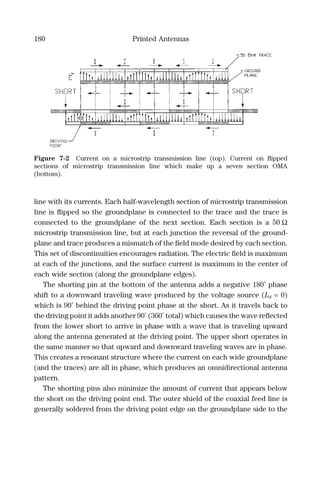
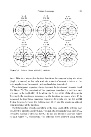
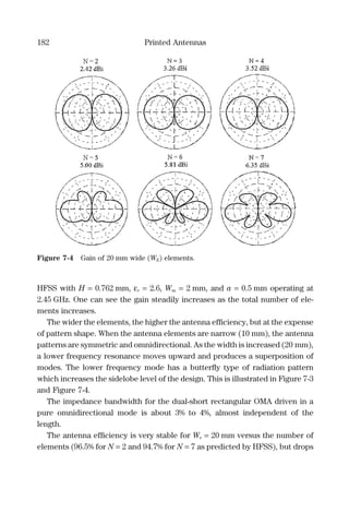
![Printed Antennas 183
with length as the number of elements is increased for We = 10 mm (91.3% for
N = 2 and 87.6% for N = 7).
A seven-section OMA was designed to operate at 2.45 GHz on 0.762 mm
(0.030 inches) laminate material. The relative dielectric constant of the sub-
strate is εr = 2.6 with tanδ = 0.0025. The dimensions of the antenna are Wm =
2.06 mm, We = 16.25 mm, Le = Lm = 36.58 mm. Shorting pins located on either
end of the antenna have a 0.5 mm radius (a). The antenna is fed with a probe
at the junction where the first narrow line and the next wide section meet (i.e.,
Ld = 0) in Figure 7-1. The dielectric material extends out 2.0 mm from each side
and 2.0 mm from each end.
The finite difference time domain (FDTD) method was used to compute the
expected radiation patterns.[8]
A sinusoidal 2.586 GHz source was utilized to
compute the radiation patterns of the antenna. They are presented in Figures
7-5(a–c) with corresponding measured radiation patterns. The best antenna
Figure 7-5 (a) The y-z plane radiation patterns of an OMA computed using FDTD
analysis (dashed) and measured (solid) for 2.586 GHz.](https://image.slidesharecdn.com/1891121731microstrip-151111163821-lva1-app6892/85/1891121731-microstrip-191-320.jpg)

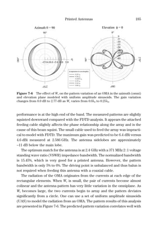
![186 Printed Antennas
HFSS computations.[9]
The predicted pattern variation value is 0.0 dB to 2.77 dB
as We ranges from 0.0λ0 to 0.25λ0.
7.1.1 Low Sidelobe Omnidirectional Microstrip Antenna
The OMA presented in Section 7.1 has a uniform illumination along its length.
A uniform amplitude distribution along an array produces sidelobes that are
−13.2 dB below the main beam. The example uniform OMA has sidelobes that
are as high as −11 dB. The uniform OMA has radiating elements of identical
widths. We can control the amount of radiation from each of the elements by
varying their widths.[10]
Figure 7-7 shows a seven-section OMA that has ele-
ments of different widths. The relative width of each element corresponds with
a −6 dB linear taper on a pedestal using equation (6.15).
Finite difference time domain analysis was used to vary the center width W4
(with the other widths dependent upon W4) until the desired distribution to
produce a −22.5 dB sidelobe level is obtained. The design uses a 0.762 mm
(0.030 inches) thick dielectric substrate with εr = 2.6 and tanδ = 0.0025. The
element widths are W1 = 3.0 mm, W2 = 7.32 mm, W3 = 11.66 mm, and W4 =
16.0 mm with 50 Ω interconnects of 2.03 mm width. The length of each element
is 36.15 mm. An antenna with the dimensions from the previous FDTD analysis
(Section 7.1) was fabricated with the altered element widths. The antenna pat-
terns were optimum at 2.628 GHz, but the input impedance has a slight series
inductive reactance which produced an unacceptable mismatch (2.5:1 VSWR).
A 1.0 pF capacitor was used as a via at the driving point to match the antenna
with a return loss of better than 25 dB. The normalized impedance bandwidth
of the matched −6 dB taper OMA is 3.8%, which is smaller than the 14.58%
bandwidth of the uniform design.
The directivity predicted by FDTD analysis is 5.39 dB. The measured gain
of the fabricated antenna is 5.0 dBi. The measured and predicted radiation
patterns are presented in Figure 7-8(a) and Figure 7-8(b).
The FDTD patterns have a −22.5 dB sidelobe level. The measured patterns
are close to the −20 dB sidelobe level. This is approximately a 9 dB improve-
ment over the −11 dB sidelobe level of the uniform OMA design.
When designing an omnidirectional antenna, it is often useful to know the
approximate directivity of an omnidirectional pattern versus the half-power](https://image.slidesharecdn.com/1891121731microstrip-151111163821-lva1-app6892/85/1891121731-microstrip-194-320.jpg)
![Printed Antennas 187
beamwidth (HPBW). Pozar developed a curve-fit equation based on a sinN
θ
pattern to relate the HPBW of an omnidirectional pattern without sidelobes to
its directivity:[11]
D
HPBW
= + −
10 191 0 0 818
1
172 410log . . . dB
Figure 7-7 Seven section OMA with linear taper.](https://image.slidesharecdn.com/1891121731microstrip-151111163821-lva1-app6892/85/1891121731-microstrip-195-320.jpg)
![188 Printed Antennas
where HPBW is the elevation-plane half-power beamwidth (in degrees). This
equation is valid up to a beamwidth of 140˚. When sidelobes are present with
an assumed uniform current distribution, McDonald has developed a relation-
ship that uses a sin(bθ)/(bθ) pattern as its basis:[12]
D
HPBW HPBW
=
−
10
101 5
0 00272
10 2
log
.
. ( )
dB
7.1.2 Element Shaping of an Omnidirectional Microstrip Antenna
The OMAs discussed thus far all have rectangular elements. The use of other
shapes can provide some advantages in the design of an OMA. Figure 7-9 shows
five combinations of circular, rectangular, and elliptical elements.
Figure 7-8 (a) Omniplane radiation patterns of a seven section OMA with linear
taper. Eφ (φ = 0) x-z plane. The dashed line is from FDTD analysis. The solid line is
measured.](https://image.slidesharecdn.com/1891121731microstrip-151111163821-lva1-app6892/85/1891121731-microstrip-196-320.jpg)

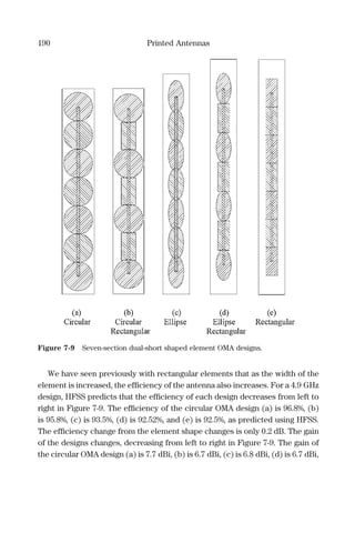
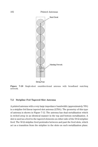


![Printed Antennas 195
plane dimensions are 60 mm × 65 mm. The stripline is 10.7 mm from the left
edge. FDTD analysis shows the antenna has a better than 2:1 VSWR [−9.54 dB
negative return loss (NRL)] from 3.19 GHz to 6.81 GHz, as shown in
Figure 7-13.
The gain of the stripline linear tapered slot antenna versus frequency is
presented in Table 7-1. Over the band of operation in Figure 7-13, the gain
ranges from 5.17 dBi to 8.87 dBi.
Figure 7-13 Negative return loss of stripline fed linear tapered slot antenna.
Table 7-1 Stripline linear tapered slot antenna example
gain versus frequency.
Frequency (GHz) Gain (dBi)
3.190 5.17
4.000 5.49
5.250 7.50
5.650 7.93
6.810 8.87](https://image.slidesharecdn.com/1891121731microstrip-151111163821-lva1-app6892/85/1891121731-microstrip-203-320.jpg)

![Printed Antennas 197
7.2.1 Stripline Fed Vivaldi Antenna
The LTSA is a special case of an exponentially tapered slot antenna (ETSA)
which was introduced by Gibson in 1979 and called the Vivaldi antenna.[13]
Vivaldi antennas have been optimized for very large impedance bandwidths
(6:1).
The taper that describes the limits of the ETSA or Vivaldi is
y AeBx
= ±
where
A
Sw
=
2
B
a S
L
w
a
=
ln( / )
and a is the antenna aperture at La and Sw is the slot width at the antenna
origin.
The exponential taper of a Vivaldi antenna is the common geometry of
several designs which differ in their method of providing a transition from
a driving point to the exponential slots. One geometry which is used to
create Vivaldi elements is presented in Figure 7-15.[14]
Metallization on either
side of the substrate of thickness H is removed to create the transition and
antenna element. A circular open circuit with a radius of R0 is attached to a
slot of length Ls and width Sw. The exponential taper begins after this slot
and extends for length LA, which is the length of the element. The aperture of
the element is a. The board length and width are L and W, respectively. The
stripline feed is of width Ws terminates in a radial stub with an angle of α and
radius Rs.
Early work on Vivaldi antennas used simpler transitions, as shown in
Figure 7-12 for the LTSA. Considerable work has been undertaken to maximize
the impedance bandwidth of the Vivaldi antenna. Figure 7-15 is a refinement](https://image.slidesharecdn.com/1891121731microstrip-151111163821-lva1-app6892/85/1891121731-microstrip-205-320.jpg)
![198 Printed Antennas
of the original transition. Another approach has been to feed the antenna
from the left side with microstrip along the centerline, narrow the microstrip
groundplane to create a balun, and form a Vivaldi notch after the balun transi-
tion between the two layers.[15]
This approach has created an antenna element
with a very wide bandwidth. A large impedance bandwidth helps to preserve
the shape of pulses required by ultra-wideband (UWB) systems. The design of
Vivaldi antennas is empirical and is suited to the use of analysis to optimize
their design prior to fabrication.
Figure 7-16 is a negative return loss plot from an FDTD analysis of a Vivaldi
antenna with geometry as defined in Figure 7-15. The antenna parameters are
W = 30.0 mm, Sw = 1.0 mm, LA = 45.0 mm, Ls = 5.0 mm, R0 = 4.5 mm, Rs = 8.0 mm,
α = 80 mm, Ws = 0.5 mm, εr = 2.2, W = 40.0 mm, L = 63.0 mm, and H = 1.524 mm.
The antenna has better than 2:1 VSWR (−9.54 dB NRL) from 2.69 GHz to
10.18 GHz.
Figure 7-15 Geometry of a Vivaldi antenna (exponential tapered slot antenna).](https://image.slidesharecdn.com/1891121731microstrip-151111163821-lva1-app6892/85/1891121731-microstrip-206-320.jpg)
![Printed Antennas 199
7.3 Meanderline Antennas
7.3.1 Electrically Small Antennas
In some applications, an electrically small planar antenna can be an appropri-
ate solution. Electrically small antennas (ESAs) have fundamental limitations
to their bandwidth. The definition of an ESA is an antenna whose maximum
dimension is less than λ/2π.[16]
This relation is often expressed as
ka < 1 (7.1)
where
k = 2π/λ (in radians/meter)
λ = free space wavelength (in meters)
a = radius of sphere enclosing the maximum dimension of the antenna (in
meters).
Figure 7-16 Negative return loss plot of the Vivaldi antenna example computed with
FDTD analysis.](https://image.slidesharecdn.com/1891121731microstrip-151111163821-lva1-app6892/85/1891121731-microstrip-207-320.jpg)

![Printed Antennas 201
In 1996 McLean refined and corrected earlier work on the minimum Q of an
ESA.[17]
The minimum Q for an electrically small linear antenna in free space
is expressed as
Q
k a ka
L = +
1 1
3 3
(7.5)
The minimum Q for an ESA that is circularly polarized is
Q
k a ka
cp = +
1
2
1 2
3 3 (7.6)
Equation (7.5) and equation (7.6) assume a perfect lossless matching
network.
The minimum Q relationship was originally derived for the case of an ESA
in free space. In any practical environment an ESA is near some type of ground-
plane or other structure. In 2001 Sten et al. evaluated the limits on the funda-
mental Q of an ESA near a groundplane.[18]
These relationships provide useful
guidelines on theoretical limits to the development of an ESA with a desired
impedance bandwidth.
The Q for the case of a horizontal current element and a vertical current
element over a groundplane are analyzed as illustrated in Figure 7-17. The for-
mulas for the Q of both instances are found in Sten et al.[18]
Figure 7-17 Vertical and horizontal ESAs (current) over a large groundplane and
their enclosing spheres.](https://image.slidesharecdn.com/1891121731microstrip-151111163821-lva1-app6892/85/1891121731-microstrip-209-320.jpg)
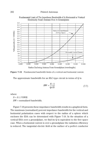


![Printed Antennas 207
FDTD results of Figure 7-21(a) and Figure 7-21(b) show the meanderline ESA
with it’s original groundplane width. The thermal plots show the magnitude of
the edge current, which correlates to the direction shown in Figure 7-20
(WG = 66.7 mm). One can see by comparison with Figure 7-21(d) that no sig-
nificant currents exist on the edges when the groundplane is widened. The
width of the electrically small matching section had to be increased
(WM = 4.8 mm) to cancel the increased capacitive reactance of the meanderline
antenna driving point as the antenna’s Q increased.
The main difference between the narrow and wide groundplane meander-
line ESA antennas is the impedance bandwidth. When the groundplane width
is increased to 66.7 mm, the bandwidth of the element decreases to 5.19% of
the bandwidth. This value is in fair agreement with our computed estimate of
7.66%. Realizing the fundamental bandwidth limit in practice has proven elusive.
Theoretical work by Thiele et al. suggests that this theoretical limit is based
on a current distribution that is not obtainable in practice.[19]
Figure 7-22 shows the computed impedance bandwidth change for the base-
line antenna groundplane width (WG = 16.7 mm) and after 25 mm of extra
groundplane are added to each side. The reduction in impedance bandwidth
is clearly illustrated.
A pair of antennas were constructed using the dimensions obtained with
FDTD analysis. Figure 7-23 shows the measured impedance bandwidth change
for the baseline antenna and with 25 mm of extra groundplane. We note the
measurements correlate very well with the predicted FDTD analysis. The mea-
sured antennas had a slightly higher resonant frequency than the analysis.
One must realize that when an ESA is used in an application, the ground-
plane and environment have a considerable affect on the bandwidth and what
the extent of the actual antenna is versus what one might assume.
7.3.2.2 Meanderline Antenna Radiation Patterns
The antenna patterns computed using FDTD analysis are nearly equivalent for
the small and large groundplane (2.0 dB directivity). Computed radiation pat-
terns for the wide groundplane case are presented in Figure 7-24. The elevation
plane radiation pattern in Figure 7-24 is similar to that of a dipole and matches
the direction of the radiating currents of Figure 7-20. The pattern is omnidirec-
tional in the x-z plane, consistent with the radiating current. FDTD modeling](https://image.slidesharecdn.com/1891121731microstrip-151111163821-lva1-app6892/85/1891121731-microstrip-215-320.jpg)
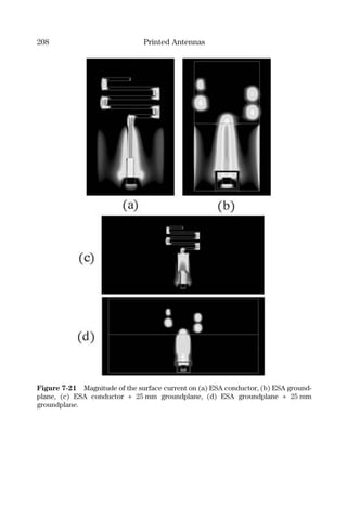

![210 Printed Antennas
allows for “perfect” feeding of the antenna, which minimizes perturbation from
a coaxial feed line.
In practice, the gain of an ESA is bounded. This limitation has been expressed
by Harrington as[20]
G ka ka= +( ) ( )2
2 (7.8)
When applied to the meanderline antenna, the maximum attainable gain for
the antenna on a large groundplane (a = 15.63 mm) is 1.13 dBi; when the
Figure 7-24 Radiation patterns of the narrow groundplane baseline (solid lines)
meanderline ESA computed with FDTD analysis and the antenna with 25 mm wide
groundplane width added (dashed lines).
Figure 7-25 The measured radiation patterns of the baseline (narrow groundplane)
meanderline ESA (dashed lines) and the antenna with 25 mm groundplane width added
(solid lines).](https://image.slidesharecdn.com/1891121731microstrip-151111163821-lva1-app6892/85/1891121731-microstrip-218-320.jpg)
![Printed Antennas 211
groundplane is reduced (a = 21.83 mm) we have a maximum possible gain of
2.9 dBi.
Meanderline antennas were fabricated and found to match at 1.655 GHz
(4.83% from 1.575 GHz). When measured, the maximum gain of the meander-
line antenna with a large groundplane is 0.3 dBi. The measured gain value of
the antenna with a smaller groundplane is 0.5 dBi. The smaller groundplane
meanderline antenna generated more current along the coaxial cable that con-
nects the antenna to the ESA than the wider antenna. This makes measuring
the small groundplane antenna in isolation difficult and adds loss. This mea-
surement problem has been noted and discussed by Staub et al.[21]
An ESA has
a combination of balanced and unbalanced modes which makes pattern mea-
surement particularly problematic when using a coaxial (unbalanced) cable to
feed the ESA.
7.4 Half-Patch with Reduced Short-Circuit Plane
In 1987 Taga et al. introduced a modified version of a half-patch (λ/4) microstrip
antenna in which the width of the shorting plane was altered to reduce the
resonant frequency of the antenna.[22]
The geometry of a planar inverted-F
(type) antenna (PIFA) is presented in Figure 7-26. The antenna is fed along
one edge at location F. The short is reduced in width with respect to the
edge opposite that of the feed to width W. The element is of dimensions
L1 and L2 and thickness H. The original PIFA uses air as its dielectric
substrate.[23]
When W = L1, the antenna becomes a quarter-wave microstrip (half-patch)
antenna (Figure 2-11). As the width W becomes small enough to be equivalent
to a shorting post, the antenna has the appearance of an inverted-F antenna
with a conductive plane attached to one side. The element was called a PIFA
from this view of the geometry.
The resonant frequency of the antenna decreases as the value of W decreases.
When W/L1 = 0.125, it has been reported that the resonant frequency is about
40% of a half-patch. When L1/L2 = 2.0, for a ratio of L1/L2 = 1.0, the resonant
frequency is about 60% of the half-patch. When L1/L2 = 0.5, it is lowered to about
70% of a normal quarter-wavelength patch antenna.](https://image.slidesharecdn.com/1891121731microstrip-151111163821-lva1-app6892/85/1891121731-microstrip-219-320.jpg)

![Printed Antennas 213
less than one. The impedance bandwidth of a PIFA can be increased by increas-
ing H, which increases the volume of the antenna.[24]
One can decrease the size
of the groundplane upon which the PIFA is constructed until the groundplane
itself becomes part of the radiating structure and increases the impedance
bandwidth.[25]
This was illustrated earlier with the meanderline antenna. One
must trade off the decrease in resonant frequency as W is decreased, with an
associated decrease in impedance bandwidth for a given application.
One can create a PIFA-type structure where the back shorting plane is cen-
tered and the feed is positioned along the centerline (CPIFA). This is illustrated
in Figure 7-28. If the width of the shorting plane is that of case A (W = 6.0 mm)
with the CPIFA geometry, the resonant frequency is a slightly higher 1.112 GHz
with 2.79% bandwidth.
When the shorting plane width is small (W << L1), the resonant frequency of
a PIFA (εr = 1) is approximately
F
c
L L
r =
+4 1 2( )
(7.9)
Figure 7-27 The negative return loss of a λ/4 microstrip antenna (baseline PIFA W =
L1) and PIFA (W = 6 mm) versus frequency.](https://image.slidesharecdn.com/1891121731microstrip-151111163821-lva1-app6892/85/1891121731-microstrip-221-320.jpg)

![Printed Antennas 215
63 mm × 63 mm groundplane. The impedance bandwidth of a PIFA with a
finite-size groundplane is generally smaller than that predicted for an infinite
groundplane. This finding is consistent with the results for a centered shorting
plane PIFA reported by Huynh and Stutzman.[26]
The movement of the 50 Ω feed point location toward the shorting plane as
W is decreased for a centered shorting plane is shown in Figure 7-30. The
results are very similar to those for the standard PIFA geometry.
In practice, a PIFA is often realized using a shorting post rather than a short-
ing plane. FDTD analysis demonstrates that as the radius of the shorting post
decreases, so does the resonant frequency. As the resonant frequency decreases,
the 50 Ω driving point position moves closer to the shorting post, as seen previ-
ously with the shorting planes.
HFSS analysis illustrates that a contour of 50 Ω driving point locations exists
for the case of a PIFA realized with a shorting post (Figure 7-31). The PIFA
dimensions H, L1, and L2 are the same as Taga’s with a 63 mm × 63 mm ground-
plane and 2 mm radius shorting post. As the shorting plane width or shorting
post radius is decreased, the location of the 50 Ω driving point can become so
close to the short as to be unrealizable.
Figure 7-29 The operating frequency of a PIFA is decreased as the width of the short-
ing plane is decreased. The edge resistance of the patch increases because the electrical
width of the antenna narrows. Because of this edge resistance increases and the loca-
tion of a 50 Ω driving point moves toward the shorting plane. This is illustrated with
electric field magnitude plots for a normal PIFA using FDTD analysis.](https://image.slidesharecdn.com/1891121731microstrip-151111163821-lva1-app6892/85/1891121731-microstrip-223-320.jpg)

![Printed Antennas 217
In many practical applications the groundplane and PIFA dimensions can
produce a driving point antiresonance that renders the antenna unrealizable.
The currents on the feed center conductor, which have upward and downward
currents that tend to cancel, can begin to couple to the PIFA shorting post/
plate. When the feed probe is close enough, the coupling increases to the point
where the current on the feed and shorting post/plate travel in phase, and in
practice produce an antiresonance.
The main advantage of using a PIFA is that it is a very compact ESA. The
majority of the radiation is from the vertical current on the shorting plane
(post) which is between two thin conductive plates. The impedance bandwidth
and gain of a PIFA are consistent with the fundamental limits of an ESA with
a vertical current as described by equation (7.5) and equation (7.8). Other
comparable printed antenna designs (such as a half slot) must be physically
thicker than a PIFA for the same effective height because the radiating length
is less than the physical height.
Alternative methods of decreasing the resonant frequency of a patch without
the use of a short exist. Slots and rectangular apertures have been cut into
rectangular microstrip antenna elements to reduce the resonant frequency.
Details of these designs may be found in the literature.[27]
7.4.1 Dual-Band PIFA
The PIFA has proved popular as a dual-band antenna for mobile devices. Often
a slot is cut into the planar conductor to create a dual-band element. A radiat-
ing and balanced mode analysis of a dual-band PIFA performed by Boyle and
Ligthart revealed important insight into this design.[28]
The dual-band PIFA
design geometry is shown in Figure 7-32. The slot introduces an additional
resonance that is proportional to the length of the slot. As the slot length
becomes approximately one-half wavelength, the currents on each side of the
slot shift from cophase to antiphase. The natural resonant mode of the radiator
is between the two modes. The proper choice of dimensions allows for dual-
band operation. A long slot is required to create a dual-band PIFA of this
geometry. The PIFA is analyzed on a circuit board which represents a mobile
device. The half-wave resonances of the circuit board need to be understood
and taken into account for a workable design.](https://image.slidesharecdn.com/1891121731microstrip-151111163821-lva1-app6892/85/1891121731-microstrip-225-320.jpg)


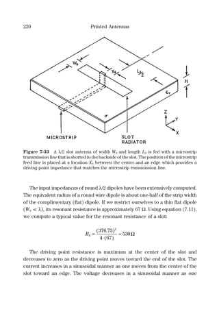
![Printed Antennas 221
moves from the center of the slot to an edge. This implies the driving point
resistance (Rdrv) will vary as[29]
R R k
L
Xdrv S
s
S≈ −
sin2
2
Ω (7.12)
This allows us to compute the approximate position of a 50 Ω (Rdrv = 50 Ω)
driving point:
X
L R
R
S
s drv
S
= − −
2 2
1λ
π
sin (7.13)
For a slot that is at resonance with Ls = 0.46λ and RS = 530 Ω, the 50 Ω driving
point location Xs is
XS = − =−0 46
2 2
50
530
0 1801.
sin .
λ λ
π
λ
which is 0.050λ from the end of the slot.
As an example rectangular slot antenna design, we use a substrate with εr
= 3.5 and a tanδ = 0.0055. The thickness of the substrate is H = 0.5 mm. The
slot dimensions are Ls = 22 mm and Ws = 1.0 mm. The feed point is Xs = 8.0 mm.
The microstrip line width is 1.0 mm.
The predicted negative return loss plot of the rectangular slot antenna is
presented in Figure 7-34. The antenna is seen to have an 18.78% (2:1VSWR)
impedance bandwidth.
The current has a maximum value along the ends of the slot radiator. These
currents are directed parallel with the yˆ axis. The electric field of the radiator
is across the narrow dimension of the slot which produces yˆ-directed polariza-
tion. The maximum driving point impedance at the center of the slot antenna
allows one to cut the slot radiator in half to produce a λ/4 version. A single
yˆ-directed current then becomes the radiation source. Further reducing the
groundplane surrounding the λ/4 slot produces a printed circuit version of an
inverted F antenna (IFA).[30]](https://image.slidesharecdn.com/1891121731microstrip-151111163821-lva1-app6892/85/1891121731-microstrip-229-320.jpg)
![222 Printed Antennas
Figure 7-35 shows the E- and H-plane radiation patterns of the example
microstrip fed slot antenna computed using FDTD analysis. The pattern direc-
tivity is 4.66 dB.
7.5.1 Microstrip Slot Antenna “Fictitious Resonance”
One may have noted the considerable bandwidth and pair of negative return
loss minimums of the previous microstrip slot antenna design example. It was
noted by Behdad and Sarabandi that a slot fed in this manner can contain two
resonances.[31,32]
The first resonance is the expected normal resonance of the
full slot, but a second “fictitious” resonance may also exist in some slot designs.
The fictitious resonance occurs when the tangential electric field component
of the feed conductor is in a position along the slot which cancels the electric
field of the slot excited by the groundplane return current. The width of the
feed line, the slot width, and the distance from the edge of the slot to the center
of the feed line (Ls) determines the existence and location of the fictitious reso-
Figure 7-34 Negative return loss (in dB) of the example slot antenna.](https://image.slidesharecdn.com/1891121731microstrip-151111163821-lva1-app6892/85/1891121731-microstrip-230-320.jpg)
![Printed Antennas 223
nance. The frequency of the fictitious resonance may be increased by increas-
ing Ls, which increases the total impedance bandwidth or produces dual-band
operation. The overall length of the slot L determines the frequency of the
lower resonance. The length of the microstrip line Lm above the slot feed con-
ductor allows for matching. The magnetic current distribution illustrated in
Figure 7-36 is similar at both resonances, producing a relatively stable radiation
pattern over the impedance bandwidth. A parametric study of the design of
this slot antenna is available in the literature.[33]
Figure 7-35 Radiation pattern of the example rectangular microstrip fed slot antenna
computed with FDTD analysis. The solid line is the E-plane pattern, the dashed line is
the H-plane pattern.](https://image.slidesharecdn.com/1891121731microstrip-151111163821-lva1-app6892/85/1891121731-microstrip-231-320.jpg)
![224 Printed Antennas
In light of the results obtained by Behdad and Sarabandi, FDTD analysis of
the design example slot antenna presented above (and in the first edition) was
undertaken at the two negative return loss minimums. A sinusoidal source was
used at 5.189 GHz and 5.744 GHz. The results are presented in Figure 7-37(a)
and Figure 7-37(b). Although the researchers indicated that a fictitious reso-
nance was best driven by using a thin conductive strip across the slot, it
appears in this case that the fictitious resonance was at work to produce a
wideband slot antenna.
This design method was implemented to create a multiband antenna for
laptop use. A half slot is used for 802.11b (2.4 to 2.5 GHz) band and a full dual-
band slot (with normal and “fictitious” resonances) covers multiple high-fre-
quency bands (4.9 to 5.875 GHz). The use of a half slot for the low band
removes the odd-numbered resonances F1, F3, . . . (F0 = 2.45 GHz) by removing
the required short-circuit boundary condition for these slot resonances. The
L
W
Lm
Ls
110 W Microstrip Feed
0.2 mm wide
50 W Microstrip Feed
Slot Antenna
L
W
Lm
110 W Microstrip Feed
0.2 mm wide
50 W Microstrip Feed
Slot Antenna
Figure 7-36 Magnetic current distribution of the normal (top) and “fictitious” (bottom)
resonance of a slot antenna fed with a narrow line from a microstrip transmission line
and impedance matched using an open microstrip line. (From [32], copyright 2004,
IEEE. Reprinted with permission.)](https://image.slidesharecdn.com/1891121731microstrip-151111163821-lva1-app6892/85/1891121731-microstrip-232-320.jpg)
![Printed Antennas 225
Figure 7-37 (a) Electric field magnitude (linear) for 5.189 GHz resonance of the
example design.
removal of the F1 resonance allows the bottom full dual-band slot antenna to
operate from 4.9 to 5.875 GHz without interference from the upper slot’s driving
point impedance.[34]
7.6 Microstrip Fed Log-Periodic Balun Printed Dipole
A printed dipole antenna fed using microstrip is illustrated in Figure 7-38.[35]
Microstrip is an unbalanced transmission line and requires a balun to produce
the desired balanced transmission line mode for the printed twin-lead transmis-
sion line, which in turn feeds the dipole. The microstrip input is at the bottom
of the figure and connects to the input port of a two-section log-periodic
microstrip balun described by Al Basraoul and Shastry.[36]
The two 50 Ω
microstrip transmission lines are of opposite phase and equal magnitude as](https://image.slidesharecdn.com/1891121731microstrip-151111163821-lva1-app6892/85/1891121731-microstrip-233-320.jpg)


![232 Printed Antennas
The tapered balun of the MFTBA produces a pattern with some beam squint,
but still reduces the current on a coaxial connection line to small values. This
dipole design is useful when a dipole is required that does not have as pure
dipole patterns as a Roberts dipole, but is required for a test fixture or other
purpose where the ease of fabrication may be of greater importance.[37–39]
References
[1] Nesic, A., and Nesic, D., “Omnidirectional uniplanar electromagnetically coupled
antenna array,” Microwave and Optical Technology Letters, March 20, 2004, Vol.
40, No. 6, pp. 516–518.
[2] Bancroft, R., and Bateman, B. “An omnidirectional microstrip antenna,” IEEE
Transactions on Antennas and Propagation, November 2004, Vol. 52, No. 11, pp.
3151–3153.
[3] Bancroft, R., “Design parameters of an omnidirectional planar microstrip antenna,”
Microwave and Optical Technology Letters, December 5, 2005, Vol. 47, No. 5, pp.
414–418.
[4] Jasik, H., Myslicki, R. L., and Rudish, R. M., “Sheet antenna array structure,” U.S.
Patent 3,757,342.
[5] Rudish, R. M., “Comments on ‘An omnidirectional planar microstrip antenna’,”
IEEE Transactions on Antennas and Propagation, November 2005, Vol. 53, No.
11, p. 3855.
[6] Hill, R., “A twin line omni-directional aerial configuration,” 8th European Micro-
wave Conference, September 1978, pp. 307–311.
[7] Ono, M., Numazaki, T., and Mizusawa, M., “A high-gain omnidirectional antenna
made of a printed element,” Transactions of the IECE of Japan, January 1980, Vol.
E63, No. 1, pp. 58–60.
[8] Yee, K. S., “Numerical solution of initial boundary value problems involving Max-
well’s equations in isotropic media,” IEEE Transactions on Antennas and Propa-
gation, May 1966, Vol. 14, No. 3, pp. 302–307.
[9] Bancroft, R., “Radiation properties of an omnidirectional planar microstrip
antenna,” Microwave and Optical Technology Letters, January 2008, Vol. 50, No.
1, pp. 55–58.
[10] Bancroft, R., and Bateman, B., “An omnidirectional microstrip antenna with low
sidelobes,” Microwave and Optical Technology Letters, July 5, 2004, Vol. 42, No.
1, pp. 68–69.
[11] Pozar, D., “Directivity of omnidirectional antennas,” IEEE Transactions on Anten-
nas and Propagation, October 1993, Vol. 35, No. 5, pp. 50–51.](https://image.slidesharecdn.com/1891121731microstrip-151111163821-lva1-app6892/85/1891121731-microstrip-240-320.jpg)
![Printed Antennas 233
[12] McDonald, N., “Omnidirectional pattern directivity in the presence of minor lobes:
revisited,” IEEE Transactions on Antennas and Propagation, April 1999, Vol. 41,
No. 2, pp. 63–65.
[13] Gibson, P. J., “The Vivaldi aerial,” 9th European Microwave Conference, Brighton,
UK, 1979, pp. 101–105.
[14] Shin, J., and Schaubert, D. H., “A parameter study of stripline-fed Vivaldi notch-
antenna arrays,” IEEE Transactions on Antennas and Propagation, May 1999,
Vol. 47, No. 5, pp. 879–886.
[15] Noronha, J. A. N., Bielawa, T., Anderson, C. R., Sweeney, D. G., Licul, S., and Davis,
W. A., “Designing antennas for UWB systems,” Microwaves & RF, June 2003, pp.
53–61.
[16] Wheeler, H. A., “Fundamental limits of small antennas,” Proceedings IRE, Decem-
ber 1947, pp. 1479–1484.
[17] McLean, J. S., “A re-examination of the fundamental limits on the radiation Q of
electrically small antennas,” IEEE Transactions on Antennas and Propagation,
May 1996, Vol. 44, No. 5, pp. 672–675.
[18] Sten, J. C.-E., Hujanen, A., and Koivisto, P. K., “Quality factor of an electrically
small antenna radiating close to a conducting plane,” IEEE Transactions on
Antennas and Propagation, May 2001, Vol. 49, No. 5, pp. 829–837.
[19] Thiele, G. A., Detweiler, P. L., and Penno, R. P., “On the lower bound of the radia-
tion Q for electrically small antennas,” IEEE Transactions on Antennas and
Propagation, June 2003, Vol. 51, No. 6, pp. 1263–1268.
[20] Harrington, R. F., “Effect of antenna size on gain, bandwidth, and efficiency,”
Journal of Research of the National Bureau of Standards-D, Radio Propagation,
January–February 1960, Vol. 64D, No. 1, pp. 1–12.
[21] Staub, O., Zurcher, J. F., and Skrivervlk, A., “Some considerations on the correct
measurement of the gain and bandwidth of electrically small antennas,” Micro-
wave and Optical Technology Letters, February 20, 1998, Vol. 17, No. 3, pp.
156–160.
[22] Taga, T., Tsunekawa, K., and Sasaki, A., “Antennas for detachable mobile
radio units,” Review of the ECL, NTT, Japan, January 1987, Vol. 35, No. 1,
pp. 59–65.
[23] Taga, T., “Analysis of planar inverted-F antennas and antenna design for portable
radio equipment,” in Analysis, Design, and Measurement of Small and Low-
Profile Antennas, Hirasawa, K., and Haneishi, M., eds., London: Artech House,
1992, pp. 160–180.
[24] Taga, T., Tsunekawa, K., and Sasaki, A., “Antennas for detachable mobile
radio units,” Review of the Electrical Communications Laboratories, Nippon
Telegraph and Telephone Corporation, Japan, January 1987, Vol. 35, No. 1, pp.
59–65.](https://image.slidesharecdn.com/1891121731microstrip-151111163821-lva1-app6892/85/1891121731-microstrip-241-320.jpg)
![234 Printed Antennas
[25] Zurcher, J. F., Staub, O., and Skrivervlk, A. K., “SMILA: a compact and efficient
antenna for mobile communications,” Microwave and Optical Technology Letters,
November 5, 2000, Vol. 27, No. 3, pp. 155–157.
[26] Huynh, M. C., and Stutzman, W., “Ground plane effects on planar inverted-F
antenna (PIFA) performance,” IEE Proceedings on Microwave, Antennas and
Propagation, August 2003, Vol. 150, No. 4, pp. 209–213.
[27] Deshmukh, A. A., and Kumar, G., “Formulation of resonant frequency for compact
rectangular microstrip antennas,” Microwave and Optical Technology Letters,
February 2007, Vol. 49, No. 2, pp. 498–501.
[28] Boyle, K. R., and Ligthart, L. P., “Radiating and balanced mode analysis of PIFA
antennas,” IEEE Transactions on Antennas and Propagation, January 2006, Vol.
54, No. 1, pp. 231–237.
[29] Milligan, T. A., Modern Antenna Design, New York: McGraw-Hill, 1985, pp. 83–84.
[30] Wong, K.-L., Planar Antennas for Wireless Communications, New York: John
Wiley & Sons, 2003, p. 10.
[31] Behdad, N., and Sarabandi, K., “A novel approach for bandwidth enhancement of
slot antennas,” Proceedings of the 2003 Antenna Applications Symposium, Allerton
Park, Monticello, IL, September 17–19, 2003, pp. 176–188.
[32] Behdad, N., and Sarabandi, K., “Dual resonator slot antennas for wireless applica-
tions,” IEEE AP-S International Symposium Digest, Monterey, CA, June 20–25,
2004.
[33] Behdad, N., and Sarabandi, K., “A wide-band slot antenna design employing a ficti-
tious short circuit concept,” IEEE Transactions on Antennas and Propagation,
January 2005, Vol. 53, No. 1, pp. 475–482.
[34] Bancroft, R., “A commercial perspective on the development and integration of an
802.11a/b/g HiperLan/WLAN antenna into laptop computers,” IEEE Antennas and
Propagation Magazine, August 2006, Vol. 48, No. 4, pp. 12–18.
[35] Bancroft, R., “Microstrip antenna,” U.S. Patent 7,098,863.
[36] Al Basraoui, M., and Shastry, P. N., “Wideband planar log-periodic balun,”
International Journal of RF and Microwave Computer-Aided Design, October
2001, Vol. 11, No. 6, pp. 343–353.
[37] Roberts, W. K., “A new wide-band balun,” Proceedings IRE, December 1957,
pp. 1628–1631.
[38] Fitzgerrell, R. C., “Standard linear antennas, 30 to 1000 MHz,” IEEE Transactions
on Antennas and Propagation, December 1986, Vol. AP-34, No. 12, p. 131.
[39] McLean, J., and Sutton, R., “The minimization of spurious radiation from the baluns
and feed regions of Roberts dipole antennas,” Antenna Measurement Techniques
Association 23rd Annual Meeting & Symposium, Denver, CO, October 21–26, 2001,
pp. 217–223.](https://image.slidesharecdn.com/1891121731microstrip-151111163821-lva1-app6892/85/1891121731-microstrip-242-320.jpg)
![Appendix A
Microstrip Antenna Substrates
A.1 Microstrip Antenna/Transmission Line Substrates
The selection of a substrate material is a balance between the required electri-
cal, mechanical, and environmental performance required by a design versus
economic constraints. Generally, if one has the available design volume to use
air as a substrate for a microstrip antenna, this is a good choice. The antenna
efficiency is high and the gain is maximized, as is the impedance bandwidth of
a conventional microstrip antenna. The surface wave loss when air is used as
a substrate is minimal.
When a dielectric substrate is selected, one is often interested in a material
with the lowest loss tangent (tan δ) available. The loss tangent is a metric of
the quantity of electrical energy that is converted to heat by a dielectric. The
lowest possible loss tangent maximizes the antenna efficiency (decreases the
losses); this was discussed in Section 2.8 of Chapter 2.
The relative dielectric constant, εr, of the substrate determines the physical
size of a patch antenna. The larger the dielectric constant, the smaller the
element size, but also the smaller the impedance bandwidth and directivity,
and the surface wave loss increases. The use of substrates with higher dielec-
tric constants also tightens fabrication tolerances.[1]
The tolerance of the dielectric value is also of significant importance in
manufacturing yield. A Monte Carlo-type analysis using the cavity model is a
good method for estimating antenna manufacturing yield for a rectangular
microstrip antenna when etching tolerance, substrate thickness tolerance, feed
point location tolerance, and dielectric tolerances are known. Substrate electri-
cal and physical parameters also vary with temperature. Recent work by
Kabacik and Bialkowski indicates that Teflon/fiberglass substrates can have
significant variations in dielectric constants for many airborne and space-borne
235](https://image.slidesharecdn.com/1891121731microstrip-151111163821-lva1-app6892/85/1891121731-microstrip-243-320.jpg)
![236 Microstrip Antenna Substrates
applications.[2]
The dielectric constants and loss tangents of Teflon and fiber-
glass often differed from what was quoted by manufacturers in their data
sheets compared with measurements and were valid over a much narrower
temperature range than encountered in many aerospace applications.
The performance variations are due to changes in the material dielectric
properties—thermal expansion had a minor effect on microstrip antenna
performance.
Generally the metal cladding attached to the dielectric substrate material is
copper. Two types of copper foil are used as cladding, rolled foil and electro-
deposited foil. Rolled foil is passed through a rolling mill a number of times
until the desired physical dimensions are obtained and is then bonded to the
substrate. Rolled copper has a polished mirror-like appearance. It is generally
used for flexible circuitry. Electrodeposited foil is created by electrodeposition
of copper onto an inert form which is generally a rolling titanium or steel drum.
A thin layer of copper is continuously removed from the form then bonded to
the substrate.[3]
Oxidation of copper traces is the primary cause of copper bond failure over
time. The copper traces oxidize on both sides (top and bottom) of the trace.
The diffusion of oxygen in the substrate material causes the bottom side of the
trace to oxidize. Continuous ambient temperatures above 250˚F will ultimately
degrade the copper bonds on the surface of the board. The most effective way
to mitigate this oxidation is to use an effective high-temperature conformal
coating. This coating will provide a barrier between the air and the surface of
the resin and copper traces.[4]
The computation of characteristic impedance and losses of a microstrip
transmission line (see Appendix C) depend on the copper foil thickness. The
copper cladding is described in terms of weight per square foot. The thickness
of the cladding may then be derived and is listed in Table A-1.[5]
Thinner copper
traces have smaller etching undercut than thicker traces. This allows for fine
(narrow) traces as compared with thicker copper. Thicker copper has higher
power-handling capability. This is important where the small cross section of
a trace could produce heat buildup and eventual failure.
Generally, the dielectric constant (εr) and loss tangent (tan δ) increase with
temperature. In space applications, moisture outgassing produces a lower
dielectric constant and loss tangent.](https://image.slidesharecdn.com/1891121731microstrip-151111163821-lva1-app6892/85/1891121731-microstrip-244-320.jpg)
![Microstrip Antenna Substrates 237
Table A-2 lists some common substrate materials used in the design of
microstrip antennas and typical dielectric constant and loss tangent values.
Teflon [polytetrafluoroethylene (PTFE)] has very desirable electrical
qualities, but is not recommended for many space applications. An extensive
discussion of PTFE substrates and their fabrication may be found in the
literature.[6]
Rexolite 1422 (cross-linked polystyrene) is among the earliest materials
used to create planar transmission line.[7]
Rexolite 1422 is a very good material
for space applications and has many desirable mechanical properties.[8]
Rexo-
lite 1422 is easily machined, and its dielectric constant remains stable up to
100 GHz. Rexolite 2200 is a fiberglass-reinforced version that has similar prop-
erties to unfilled Rexolite 1422, but it is more rigid and dimensionally stable.
Noryl (modified polyphenylene oxide) is suitable for many commercial micro-
wave applications. It has a much lower loss than FR-4 and is relatively cost
effective, but it is soft and melts at a relatively low temperature, which can
create soldering complications, and sometimes has unsuitable mechanical
properties for some applications.
Table A-1 Standard copper foil weights and foil
thicknesses.
Foil Weight Foil Thickness
1/2 oz (14 g) 0.0007 in (0.01778 mm)
1 oz (28 g) 0.0014 in (0.03556 mm)
2 oz (57 g) 0.0028 in (0.07112 mm)
4 oz (142 g) 0.0056 in (0.14224 mm)
Table A-2 Common substrate materials.
Material εr tanδ
Teflon (PTFE) 2.1 0.0005
Rexolite 1422 2.55 0.0007
Noryl 2.6 0.0011
FR-4 4.1 0.02
Alumina (99.5%) 9.8 0.0003](https://image.slidesharecdn.com/1891121731microstrip-151111163821-lva1-app6892/85/1891121731-microstrip-245-320.jpg)
![238 Microstrip Antenna Substrates
FR-4 is inexpensive and is used in many commercial applications (usually
below 1 GHz).2
FR-4 can be used for some wireless applications, but great care
must be taken to budget and minimize the losses when it is used as a substrate
above 1 GHz. The dielectric constant of FR-4 formulations varies considerably
from 3.9 to 4.6.[9]
Alumina has desirable microwave properties for applications that require a
relatively high dielectric constant (εr ≈ 10.0) and a low loss tangent. Its draw-
backs are the difficulty involved in machining it and its brittleness. Alumina has
good thermal conductivity, and in some aerospace applications it more readily
dissipates heat and remains cooler than other common microwave substrates.
In some missile applications where high temperatures may compromise solder
joints, alumina is a viable option for the dissipation of heat. Alumina’s dielectric
constant is very sensitive to the processing used to produce it.
All commercially available substrates and laminates have different require-
ments for processing. Details of fabrication issues and methods can be found
in the literature and directly from manufacturers.[10]
Other fabrication options,
such as screen printing conductive inks directly on substrates, have also been
investigated.[11]
In some commercial applications a planar antenna may be enclosed in an
injection-molded radome. The dielectric properties of the resins used are a very
important consideration in injection-molded radome design. The resin should
have known moisture absorption characteristics. Low moisture absorption is
important in maintaining a stable resonance frequency and loss characteristics
in environments that have humidity changes.
Plastic materials commonly are of two types: thermoset and thermoplastic.
When exposed to heat, thermoset materials undergo a chemical change that is
irreversible. When reheated, thermoset materials do not melt, but generally
begin charring. FR-4 is an example of a substrate made from a thermoset mate-
rial. When exposed to heat, thermoplastic materials melt, but do not undergo
an irreversible chemical change. They may be remelted after molding. Thermo-
plastic materials can be reprocessed a number of times, however, the polymer
will degrade after a large number of reprocessing cycles. Noryl is an example
of a thermoplastic substrate.
2
FR-4 is a flame retardant version of G-10. FR-4 can generally be used in applications which call
for G-10, but G-10 should not be used when FR-4 is specified. G-10 and FR-4 are rated at 285˚F.
FR-4 does not melt above its rated temperature, but instead begins charring.](https://image.slidesharecdn.com/1891121731microstrip-151111163821-lva1-app6892/85/1891121731-microstrip-246-320.jpg)
![Microstrip Antenna Substrates 239
When glass is drawn into thin fibers (which can be 1/100 the width of a
human hair) it becomes flexible enough to combine into a yarn.[12]
These yarns
may then be woven into a fiberglass cloth. A common glass cloth is Type 7628,
in which each filament is specified to have a diameter of 9.40 µm (0.37 mil).
Each yarn has 408 filaments. When woven into cloth, Type 7628 is 44 yarns/inch
(warp) × 32 yarns/inch (weft). Therefore this glass cloth has 17,952 filaments/
inch (warp) × 13,056 filaments/inch. The typical thickness of Type 7628 is 0.006
to 0.0078 inches. Ten layers of Type 7628 material can be impregnated with a
resin, then stacked and laminated to create a 0.062 inch thick woven fiberglass
material.
Type 7628 is created using E-glass, which is an electrical-grade glass.[13]
This
is considered a general-purpose glass fiber. The relative dielectric constant is
εr = 6.1 at 10 GHz with a tan δ = 0.0026.[14]
The effective dielectric constant of
the material depends on the ratio of the fiberglass to the material impregnated
into the glass cloth. In the case where Teflon (PTFE) is filled to produce a
dielectric constant of 6.0, the laminate is almost isotropic. This is because
E-glass has a dielectric constant of 6.1 and the material consists of mostly glass
fibers.[15]
Figure A-1 Cross section of ½ inch thick FR-4 showing the resin (dark) and glass
cloth (lighter) layers.](https://image.slidesharecdn.com/1891121731microstrip-151111163821-lva1-app6892/85/1891121731-microstrip-247-320.jpg)
![240 Microstrip Antenna Substrates
When fiberglass is being drawn, air bubbles may be present in the
glass, which end up as capillaries in the glass fibers. These are often referred
to as “hollow fibers.” These hollow fibers can provide a conductive path
which can create a conductive filament and possibly lead to board
failure.[16,17]
Microwave Substrate Manufacturers
Arlon
1100 Governor Lea Road
Bear, DE 19701
(302) 834-2100
www.arlonmed.com
CoorsTek
17750 W. 32nd Avenue
Golden, Co 80401
(303) 277-4779
www.coorsceramics.com
Park Electrochemical Corporation (ParkNelco)
5 Dakota Drive
Lake Success, NY 11042
(516) 354-4100
www.parknelco.com
Polyflon Company
One Willard Road
Norwalk, CT 06851
(203) 840-7555
www.polyflon.com
Rogers Corporation
One Technology Drive
P.O. Box 188
Rogers, CT 06263-0188
(860) 779-9605
www.rogerscorporation.com](https://image.slidesharecdn.com/1891121731microstrip-151111163821-lva1-app6892/85/1891121731-microstrip-248-320.jpg)
![Microstrip Antenna Substrates 241
Sheldahl
1150 Sheldahl Road
Northfield, MN 55057
(507) 663-8000
www.sheldahl.com
Taconic Advanced Dielectric Division
136 Coonbrook Road
Petersburgh, NY 12138
(518) 658-3202
www.taconic-add.com
References
[1] James, J. R., Henderson, A., and Hall, P. S., “Microstrip antenna performance is
determined by substrate constraints,” Microwave System News (MSN), August
1982, pp. 73–84.
[2] Kabacik, P., and Bialkowski, M. E., “The temperature dependence of substrate
parameters and their effect on microstrip antenna performance,” IEEE Transac-
tions on Antennas and Propagation, June 1999, Vol. 47, No. 6, pp. 1042–1049.
[3] James, J. R., and Hall P. S., eds., Handbook of Microstrip Antennas, Vol. 2,
Stevenage, UK: Peter Peregrinus, Ltd., 1989, chap. 15.
[4] Guiles, C. L., Everything You Ever Wanted To Know About Laminates . . . But
Were Afraid To Ask, 8th ed., Version 3.0, Rancho Cucamonga, CA: Arlon Inc.,
2000.
[5] Bahl, I. J., and Bhartia, P., Microstrip Antennas, London: Artech House, 1980,
Appendix C.
[6] James, J. R., and Hall, P. S., eds., Handbook of Microstrip Antennas, Vol. 2,
Stevenage, UK: Peter Peregrinus, Ltd., 1989, chap. 15.
[7] Howe, Jr., H., “Dielectric material development,” Microwave Journal, November
1978, pp. 39–40.
[8] Bouquet, F. L., Price, W. E., and Newell, D. M., “Designer’s guide to radiation effects
on materials for use on Jupiter fly-bys and orbiters,” IEEE Transactions on Nuclear
Science, August 1979, Vol. NS-26, No. 4, pp. 4660–4669.
[9] Wang, C., “Determining dielectric constant and loss tangent in FR-4,” UMR EMC
Laboratory Technical Report TR00-1-041, University of Missouri, Rolla, MO, March
2000.](https://image.slidesharecdn.com/1891121731microstrip-151111163821-lva1-app6892/85/1891121731-microstrip-249-320.jpg)
![242 Microstrip Antenna Substrates
[10] Laverghetta, T. S., Microwave Materials and Fabrication Techniques, 3rd ed.,
London: Artech House, 2000.
[11] Bancroft, R., “Conductive ink a match for copper antenna,” Microwaves & RF,
February 1987, Vol. 26, No. 2, pp. 87–90.
[12] Lamm, M., “The fiberglass story,” Invention and Technology, Spring 2007,
pp. 8–16.
[13] Wallenberger, F. T., Watson, J. C., and Li, H., “Glass fibers,” in ASM Handbook,
Vol. 21, Composites (#06781G), www.asminternational.org.
[14] Hartman, D., Greenwood, M., and Miller, D., “High strength glass fibers,” Technical
Paper, AGY Inc., 1996, Table 3.
[15] Olyphant, M., and Nowicki, T. E., “MIC substrates—a review,” Paper prepared for
presentation at ELECTRO-80, May 13, 1980, Boston, MA, p. 5.
[16] Rogers, K., Van Den Driessche, P., and Pecht, M., “Do you know that your laminates
may contain hollow fibers?,” Printed Circuit Fabrication, April 1999, Vol. 22.
No. 4, pp. 34–38.
[17] Rogers, K., Hillman, C., and Pecht, M., “Hollow fibers can accelerate conductive
filament formation,” ASM International Practical Failure Analysis, August 2001,
Vol. 1, No. 4, pp. 57–60.](https://image.slidesharecdn.com/1891121731microstrip-151111163821-lva1-app6892/85/1891121731-microstrip-250-320.jpg)