Downloaded 1,146 times
![ECM 521 TECHNICAL REPORT 2011
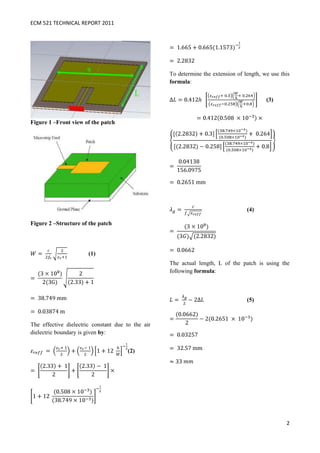
Design of a Rectangular Microstrip Patch
Antenna
cost. The selection of microstrip antenna
technology can fulfill these requirements [3].
Abstract— Throughout this technical report, WLAN in the 2.4 GHz band(2.4-2.483 GHz) has
it will briefly describe the design of a made rapid progress and severalIEEE standards
rectangular patch antenna in free space as are available namely 802.11a, b, g and j[1].
required aided with special software. The Various design techniques using defected ground
software used is Computer Simulation structure (DGS) in the patch antenna have been
Technology 2011(CST). Based on an ordinary suggested in previous publications [2-4]. DGS is
patch antenna, the antenna has isolated realized by etching a defect in the ground plane of
triangle gaps and crossed strip-line gaps etched planar circuits and antennas. This defect disturbs
on the metal patch and ground plane, the shield current distribution in the ground plane
respectively. Demonstrated to have left-handed and modifies a transmission line such as line
characteristics, the patterned metal patch and capacitance and inductance characteristics [6].
finite ground plane form a coupled capacitive- Accordingly, a DGS is able to provide a wide
inductive circuit of negative index band-stop characteristic in some frequency bands
metamaterial. It is shown to have great impact with a reduced number of unit cells. Due to their
on the antenna performance enhancement in excellent pass and rejection frequency band
terms of the bandwidth significantly broadened characteristics [6], DGS circuits are widely used
from a few hundred MHz to a few GHz, and in various active and passive microwave and
also in terms of high efficiency, low loss and millimeter-wave devices [7]. The purpose of this
low voltage standing wave ratio.Experimental work is to design and enhance a rectangular
data show a reasonably good agreement microstrip patch antenna using the parameters
between the simulation and measured results. given.
This antenna has strong radiation in the
horizontal direction for some specifical
applications within the entire band.The
simulation and results that were going to be II. METHODOLOGY
discussed in this report was based on the
parameter value given as such that the A. Review Stage
frequency is 3(GHz) with the material type of
RT/Duroid 5870 while the value of permittivity To begin with, the dimensions of the rectangular
is 2.33. Besides that the given value of substrate patch were calculated using formulae as being
thickness(mm) and copper thickness(mm) is shown below.The width is critical in terms of
0.508 and 0.035 respectively. power efficiency, antenna impedance
andbandwidth. It is largely dependent on the
operating frequency and the substrate
Keywords—Patch antenna, microstrip, CST, dielectricconstant. The equation (1) below was
permittivity, fringing effect, return loss used to work out the width of the patch. Other
widthscould have been used but if it is too small
then radiator efficiency will suffer and if it istoo
I. INTRODUCTION large higher order modes will be excited, resulting
in field distortions [1, pg-57].
icrostrip patch antenna antenna used to send
onboard parameters of article to the ground
Mwhile under operating conditions. such as
Wireless local area networks (WLAN), mobile
and sets require lightweight, small size and low
1](https://image.slidesharecdn.com/share-120427032615-phpapp01/85/Design-of-a-rectangular-patch-antenna-1-320.jpg)
![ECM 521 TECHNICAL REPORT 2011
Design of a Rectangular Microstrip Patch
Antenna
cost. The selection of microstrip antenna
technology can fulfill these requirements [3].
Abstract— Throughout this technical report, WLAN in the 2.4 GHz band(2.4-2.483 GHz) has
it will briefly describe the design of a made rapid progress and severalIEEE standards
rectangular patch antenna in free space as are available namely 802.11a, b, g and j[1].
required aided with special software. The Various design techniques using defected ground
software used is Computer Simulation structure (DGS) in the patch antenna have been
Technology 2011(CST). Based on an ordinary suggested in previous publications [2-4]. DGS is
patch antenna, the antenna has isolated realized by etching a defect in the ground plane of
triangle gaps and crossed strip-line gaps etched planar circuits and antennas. This defect disturbs
on the metal patch and ground plane, the shield current distribution in the ground plane
respectively. Demonstrated to have left-handed and modifies a transmission line such as line
characteristics, the patterned metal patch and capacitance and inductance characteristics [6].
finite ground plane form a coupled capacitive- Accordingly, a DGS is able to provide a wide
inductive circuit of negative index band-stop characteristic in some frequency bands
metamaterial. It is shown to have great impact with a reduced number of unit cells. Due to their
on the antenna performance enhancement in excellent pass and rejection frequency band
terms of the bandwidth significantly broadened characteristics [6], DGS circuits are widely used
from a few hundred MHz to a few GHz, and in various active and passive microwave and
also in terms of high efficiency, low loss and millimeter-wave devices [7]. The purpose of this
low voltage standing wave ratio.Experimental work is to design and enhance a rectangular
data show a reasonably good agreement microstrip patch antenna using the parameters
between the simulation and measured results. given.
This antenna has strong radiation in the
horizontal direction for some specifical
applications within the entire band.The
simulation and results that were going to be II. METHODOLOGY
discussed in this report was based on the
parameter value given as such that the A. Review Stage
frequency is 3(GHz) with the material type of
RT/Duroid 5870 while the value of permittivity To begin with, the dimensions of the rectangular
is 2.33. Besides that the given value of substrate patch were calculated using formulae as being
thickness(mm) and copper thickness(mm) is shown below.The width is critical in terms of
0.508 and 0.035 respectively. power efficiency, antenna impedance
andbandwidth. It is largely dependent on the
operating frequency and the substrate
Keywords—Patch antenna, microstrip, CST, dielectricconstant. The equation (1) below was
permittivity, fringing effect, return loss used to work out the width of the patch. Other
widthscould have been used but if it is too small
then radiator efficiency will suffer and if it istoo
I. INTRODUCTION large higher order modes will be excited, resulting
in field distortions [1, pg-57].
icrostrip patch antenna antenna used to send
onboard parameters of article to the ground
Mwhile under operating conditions. such as
Wireless local area networks (WLAN), mobile
and sets require lightweight, small size and low
1](https://image.slidesharecdn.com/share-120427032615-phpapp01/75/Design-of-a-rectangular-patch-antenna-1-2048.jpg)
![ECM 521 TECHNICAL REPORT 2011
B. Final Stage as calculated previously was used to calculate
the value of conductance as shown below;
(7)
(6)
where
(6-a)
0 0 sin 3 (8)
Where using the asymptotic methods [5] that it
can be shown as following ;
So,
The calculated is then being referred to
APPENDIX : Cosine and Sine Integrals [5].
To find the value of , we use equation below;
(9)
Therefore, solve for equation (6) ;
(10)
3](https://image.slidesharecdn.com/share-120427032615-phpapp01/85/Design-of-a-rectangular-patch-antenna-3-320.jpg)
![ECM 521 TECHNICAL REPORT 2011
Using the CST2011 software, is then
calculated, and the value obtained is 1.5218.
III. RESULT AND DISCUSSION
The software used to design and simulate the Figure 4 –the S-parameter diagram
microstrip patch antenna can be used to calculate
Based on the figure above, the S-
and plot S11 parameters, VSWR, radiation pattern
parameter is not achieved -10dB which is the ideal
and others.
magnitude. The return loss for this figure is :
The figures below were the results on
20 log10 S11 = -2.6
designing the microstrip patch antenna with the
given specifications. S11 = 0.7413
Figure 5 –Farfield pattern of the patch
Figure 3 –Top view of the designated patch
The patch’s radiation at the fringing field
Scattering parameter ( S- Parameter ) is used to results in a certain far-field radiation patterns. The
model N-Port linear electrical networks. For N = figure above shows that the antenna radiates more
1, S-Matrix is [S11] consists of single element. [S11 power in the red area (z-axis) than another
] parameter also known as Reflection Coefficient. direction. The directivity of this antenna is
It is a complex number that has magnitude and 7.057dBi.The IEEE standard is for an antenna to
phase angle. When magnitude of S11 is expressed have a -10dB S-parameter magnitude. The
in decibels, is known as return loss at the input scattering parameter shown above shows that the
and it always in decibels. It can be expressed by: curve falls at a frequency of 2.98GHz which is
RLinput = 20 log10 |S11| dB near enough to 3GHz as given in the specification.
The nearest to its frequency, the better the
performance as it has a sharper curve and a lower
S-parameter magnitude in dB. A lower dB
indicates the antenna having a greater directivity
4](https://image.slidesharecdn.com/share-120427032615-phpapp01/85/Design-of-a-rectangular-patch-antenna-4-320.jpg)
![ECM 521 TECHNICAL REPORT 2011
and gain.A DGS unit cell is a defect in the ground Now, the S-Parameter achieved -10dB as the
plane of a physical transmission line be it minimum ideal of parameter. By formula of return
microstrip, coplanar waveguide or whatever loss shows before, the return loss is calculated as:
structure where a reference ground plane
conductor exists, which is capable of producing a 20log S11 = -10.98dB
transmission zero in the response of the structure. S11 = 0.282
The resonant frequency of this transmission zero
depends on the physical dimensions of the defect. As we compared the value of the return loss
The main advantage of DGS, that it is easier to before and after done the DGS, the return loss
model and therefore to use in more complex after is less than before doing the DGS. The
structures. The first DGS structure is the well- smaller the value of the return loss, the smaller the
known dumbbell shaped DGS, published in 1998 reflected power due to we want the maximum
[8]. The use of a DGS (slot in the ground plane) power transferred. So when there are less loss in
allows the apparition of a stop band controlled by the antenna, it will achieve best performance of
tuning the dimensions of the slot. The ground radiation and high gain as well.
plate which has a strong E-Field is cut away in
order to get the better bandwidth.
Figure 9 –Farfield pattern after DGS
IV. CONCLUSION
Figure 7 –E-field resulted after DGS
From the analysis as above, it can be
concluded that the greater substrate thickness will
get a greater gain and directivity. The results
demonstrated that the radiation properties of the
antenna with DGS is better performance than the
antenna without DGS as the S-parameter is
measured to below than -10dB. It is also shown
that DGS have an effectto the performance of the
antenna characteristics.As the dielectric constant
of the substrate increase, the antenna bandwidth
decrease and therefore decrease the impedance
bandwidth.
Figure 8 –The S-parameter after DGS
5](https://image.slidesharecdn.com/share-120427032615-phpapp01/85/Design-of-a-rectangular-patch-antenna-5-320.jpg)
![ECM 521 TECHNICAL REPORT 2011
V. RECOMMENDATIONS Suppression For Microstrip Patch Antennas”,
Microwave and Optical Technology Letters, pp.
Microstrip patch antennas radiate primarily 103-105 Vol. 49, No. 1, January 2007.
because of the fringing fields between the patch
edge and the ground plane. For a good [3] Haiwen Liu, Zhengfan Li, Xiaowei Sun, and
performance of antenna, a thick dielectric Junfa, “Harmonic Suppression With Photonic
substrate having a low dielectric constant is Bandgap and Defected Ground Structure for a
necessary since it provides larger bandwidth,
Microstrip Patch Antenna”, IEEE Microwave and
better radiation and better efficiency. However, it
Wireless Components Letters, VOL. 15, NO. 2,
leads to a larger antenna size. In order to reduce
the size of the Microstrip patch antenna, substrates Feb. 2005.
with higher dielectric constants must be used
[4] Y. J. Sung, M. Kim, and Y.-S. Kim,
which are less efficient and result in narrow
bandwidth. Hence a trade-off must be realized “Harmonics Reduction With Defected Ground
between the antenna performance and antenna Structure for a Microstrip Patch Antenna”, IEEE
dimensions Antennas and Wireless Propagation Letters, VOL.
2, 2003.
[5] Constantine A. Balanis, “Antenna Theory Analysis
And Design”, 3rdedition , page 811-842
VI. ACKNOWLEDGMENT
[6] D. Ahn, J. S. Park, C. S. Kim, J. Kim, Y. Qian,
In the name of Allah s.w.t and He most
and T. Itoh, “A design of the low-pass filter using
merciful with Salawat and salam to prophet
Muhammad s.a.w, Alhamdulillah thanks to Him the novel microstrip defected ground structure,”
with the help and His permission giving us the IEEE Trans. Microwave Theory Tech., vol. 49,
idea and health, also the opportunity to pp. 86–93, Jan. 2001.
successfully completed this project entitled
“Design of A Rectangular Patch Antenna Using [7] C. S. Kim, J. S. Park, D. Ahn, and J. B. Lim,
CST”for Computer Engineering System Design “A novel 1-D periodic defected ground structure
subject within the given time duration. for planar circuits,” IEEE Microwave Guided
Wave Lett., vol. 10, pp. 131–133, Apr.2000.
Here, we would to express our great
thankful wishes to all of those who have been
[8] J. I. Park, C. S. Kim, J. Kim, J. S. Park, Y.
very supporting and helpful to us especially our
Antenna and Propagation lecturer, Pn.Nor Qian, D. Ahn, and T. Itoh,―Modeling of a
Hasimah Baba for her guidance, advices,and photonic bandgap and its application for the low-
monitoring us to complete this project. Special pass filter design,‖ Proceedings of Asia Pacific
thanks also to all classmates of EE2405A and Microw. Conf. (APMC), pp. 331–334, Singapore
other friends who are involved directly or 1999.
indirectly to accomplish this task. The full and
kindness of support, attention, time and advises
gives a full memories to me.
VII. REFERENCES
[1] Bahl, I. J and Bhartia, P; “Microstrip
Antennas”, Artech House, 1980.
[2] M. K. Mandal, P. Mondal, S. Sanyal, and A.
Chakrabarty , “An Improved Design Of Harmonic
6](https://image.slidesharecdn.com/share-120427032615-phpapp01/85/Design-of-a-rectangular-patch-antenna-6-320.jpg)

This technical report describes the design of a rectangular microstrip patch antenna using CST simulation software. The key steps included: 1) Calculating the antenna dimensions using standard formulas based on the given parameters of 3GHz frequency, 2.33 permittivity, 0.508mm substrate thickness. 2) Simulating the antenna in CST to analyze the S-parameters, radiation pattern, return loss. The results showed a return loss above -10dB, indicating room for improvement. 3) Etching defected ground structures (DGS) on the patch and ground plane to perturb the current and modify the transmission characteristics. 4) Simulating the modified antenna, which showed significantly improved results with a return


