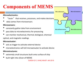
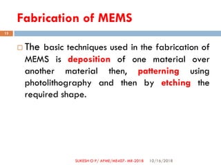
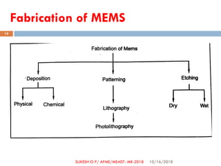
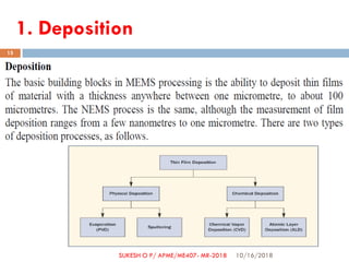
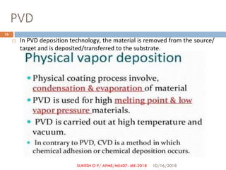
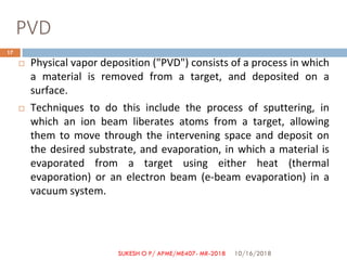
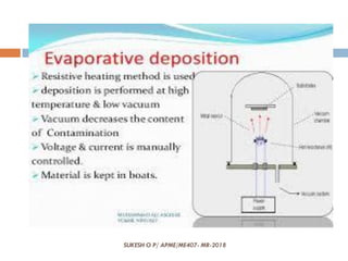
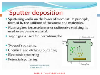
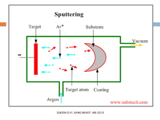
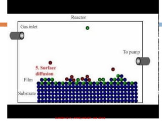
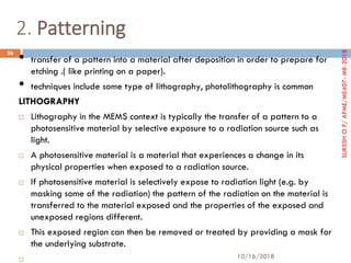
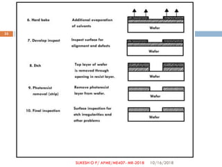
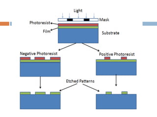
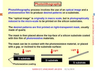
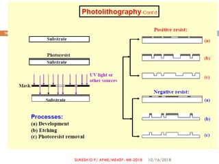
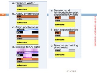
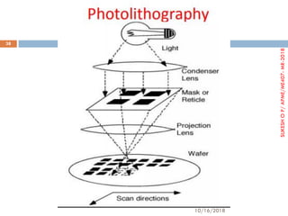
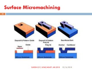
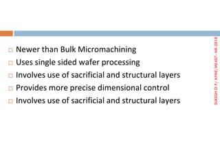
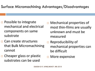
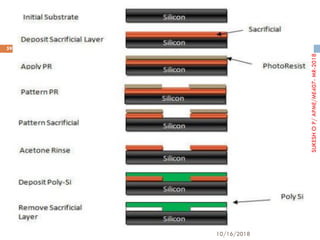
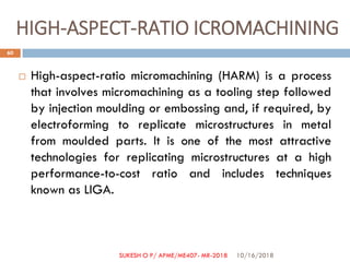
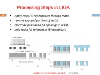
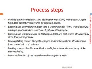
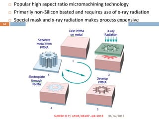
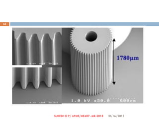
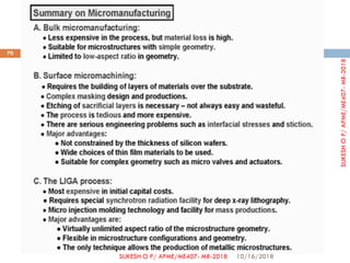
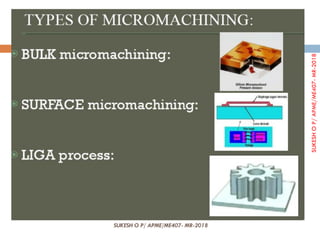
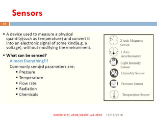
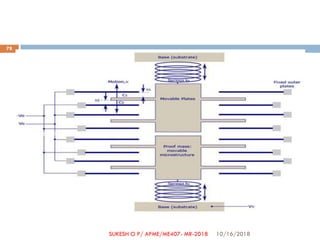
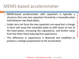
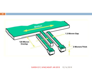
ME407 MECHATRONICS
SUKESH O P
Assistant Professor
Dept. of Mechanical Engineering
JECC
10/16/2018
1SUKESH O P/ APME/ME407- MR-2018
SUKESH O P/ APME/ME407- MR-2018
ME407 MECHATRONICS
 Course Objectives:
To introduce the features of various sensors used in CNC machines and
robots
To study the fabrication and functioning of MEMS pressure and inertial
sensors
To enable development of hydraulic/pneumatic circuit and PLC
programs for simple applications
10/16/2018
2
SUKESH O P/ APME/ME407- MR-2018SUKESH O P/ APME/ME407- MR-2018
Expected outcome:
The students will be able to
i. Know the mechanical systems used in mechatronics ii. Integrate
mechanical, electronics, control and computer engineering in the
design of mechatronics systems
ME407 MECHATRONICS
10/16/2018
3
SUKESH O P/ APME/ME407- MR-2018SUKESH O P/ APME/ME407- MR-2018
Expected outcome:
The students will be able to
i. Know the mechanical systems used in mechatronics ii. Integrate
mechanical, electronics, control and computer engineering in the
design of mechatronics systems
ME407 MECHATRONICS
10/16/2018
4
SUKESH O P/ APME/ME407- MR-2018SUKESH O P/ APME/ME407- MR-2018
SYLLABUS
 Introduction to Mechatronics, sensors, Actuators, Micro Electro
Mechanical Systems (MEMS), Mechatronics in Computer Numerical
Control (CNC) machines, Mechatronics in Robotics-Electrical drives,
Force and tactile sensors, Image processing techniques, Case studies
of Mechatronics systems.
10/16/2018
5
SUKESH O P/ APME/ME407- MR-2018
MODULE-III
 Micro Electro Mechanical Systems (MEMS): Fabrication:
Deposition, Lithography, Micromachining methods for
MEMS, Deep Reactive Ion Etching (DRIE) and LIGA processes.
Principle, fabrication and working of MEMS based pressure
sensor, accelerometer and gyroscope
10/16/2018
6
SUKESH O P/ APME/ME407- MR-2018
MEMS
 It is a technology that in its most general form can be defi
ned as miniatured mechanical and electro-mechanical ele
ments that are made using techniques of micromachining.
 Made up of components between 1-100 micrometers in si
ze (i.e., 0.001 to 0.1mm) and MEMS devices range in size
from 20micrometers to millimeter(0.02 to 1.0mm)
 Used for sensing, actuation or are passive micro-structures
 Usually integrated with electronic circuitry for control and
/or information processing
10/16/2018
7
SUKESH O P/ APME/ME407- MR-2018
Components of MEMS
Microelectronics:
• “brain” that receives, processes, and makes decisions
• data comes from microsensors
Microsensors:
• constantly gather data from environment
• pass data to microelectronics for processing
• can monitor mechanical, thermal, biological, chemical
optical, and magnetic readings
Microactuator:
• acts as trigger to activate external device
• microelectronics will tell microactuator to activate device
Microstructures:
• extremely small structures built onto surface of chip
• built right into silicon of MEMS
SUKESH O P/ APME/ME407- MR-2018
10/16/2018
9
SUKESH O P/ APME/ME407- MR-2018
Advantages of MEMS
 Better stability and higher accuracy in the performance.
 Miniaturization.
 Integration of sensors and electronics on the same
device.
 Mass fabrication at low cost.
10/16/2018
10
SUKESH O P/ APME/ME407- MR-2018
Applications of MEMS
10/16/2018
11
SUKESH O P/ APME/ME407- MR-2018
Applications of MEMS
10/16/2018
12
SUKESH O P/ APME/ME407- MR-2018
Fabrication of MEMS
 The basic techniques used in the fabrication of
MEMS is deposition of one material over
another material then, patterning using
photolithography and then by etching the
required shape.
10/16/2018
13
SUKESH O P/ APME/ME407- MR-2018
Fabrication of MEMS
10/16/2018
14
SUKESH O P/ APME/ME407- MR-2018
1. Deposition
10/16/2018
15
SUKESH O P/ APME/ME407- MR-2018
PVD
 In PVD deposition technology, the material is removed from the source/
target and is deposited/transferred to the substrate.
10/16/2018
16
SUKESH O P/ APME/ME407- MR-2018
PVD
 Physical vapor deposition ("PVD") consists of a process in which
a material is removed from a target, and deposited on a
surface.
 Techniques to do this include the process of sputtering, in
which an ion beam liberates atoms from a target, allowing
them to move through the intervening space and deposit on
the desired substrate, and evaporation, in which a material is
evaporated from a target using either heat (thermal
evaporation) or an electron beam (e-beam evaporation) in a
vacuum system.
10/16/2018
17
SUKESH O P/ APME/ME407- MR-2018
CVD
 Chemical vapor deposition (CVD) is a deposition method used
to produce high quality, high-performance, solid materials,
typically under vacuum. The process is often used in
the semiconductor industry to produce thin films.
 Chemical deposition techniques include chemical vapor
deposition ("CVD"), in which a stream of source gas reacts on
the substrate to grow the material desired.
 This can be further divided into categories depending on the
details of the technique, for example, LPCVD (Low Pressure
chemical vapor deposition) and PECVD (Plasma-enhanced
chemical vapor deposition).
10/16/2018
22
SUKESH O P/ APME/ME407- MR-2018
10/16/2018
24
SUKESH O P/ APME/ME407- MR-2018
2. Patterning
• transfer of a pattern into a material after deposition in order to prepare for
etching .( like printing on a paper).
• techniques include some type of lithography, photolithography is common
LITHOGRAPHY
 Lithography in the MEMS context is typically the transfer of a pattern to a
photosensitive material by selective exposure to a radiation source such as
light.
 A photosensitive material is a material that experiences a change in its
physical properties when exposed to a radiation source.
 If photosensitive material is selectively expose to radiation light (e.g. by
masking some of the radiation) the pattern of the radiation on the material is
transferred to the material exposed and the properties of the exposed and
unexposed regions different.
 This exposed region can then be removed or treated by providing a mask for
the underlying substrate.

10/16/2018
26
SUKESHOP/APME/ME407-MR-2018
LITHOGRAPHY
 Lithography in the MEMS context is typically the transfer of a
pattern to a photosensitive material by selective exposure to a
radiation source such as light.
 A photosensitive material is a material that experiences a
change in its physical properties when exposed to a radiation
source.
 If photosensitive material is selectively expose to radiation light
(e.g. by masking some of the radiation) the pattern of the
radiation on the material is transferred to the material exposed
and the properties of the exposed and unexposed regions
different.
 This exposed region can then be removed or treated by
providing a mask for the underlying substrate.
10/16/2018
27
SUKESH O P/ APME/ME407- MR-2018
10/16/2018
28
SUKESH O P/ APME/ME407- MR-2018
 In lithography for micromachining, the photosensitive material
used is typically a photoresist (also called resist, other
photosensitive polymers are also used).
 When resist is exposed to a radiation source of a specific a
wavelength, the chemical resistance of the resist to developer
solution changes. If the resist is placed in a developer solution
after selective exposure to a light source, it will etch away one
of the two regions (exposed or unexposed).
 If the exposed material is etched away by the developer and
the unexposed region is resilient, the material is considered to be
a positive resist. If the exposed material is resilient to the
developer and the unexposed region is etched away, it is
considered to be a negative resist.
10/16/2018
29
SUKESH O P/ APME/ME407- MR-2018
10/16/2018
30
SUKESH O P/ APME/ME407- MR-2018
10/16/2018
31
SUKESH O P/ APME/ME407- MR-2018
10/16/2018
32
SUKESH O P/ APME/ME407- MR-2018
SUKESHOP/APME/ME407-MR-2018
10/16/2018
33
SUKESH O P/ APME/ME407- MR-2018
10/16/2018
35
SUKESH O P/ APME/ME407- MR-2018
SUKESHOP/APME/ME407-MR-2018
10/16/2018
36
SUKESH O P/ APME/ME407- MR-2018
10/16/2018
37
SUKESHOP/APME/ME407-MR-2018
10/16/2018
38
SUKESHOP/APME/ME407-MR-2018
 Few lithography techniques are:
 Ion beam lithography
 Ion track technology
 X-ray lithography
10/16/2018
39
SUKESH O P/ APME/ME407- MR-2018
3. Etching
 Etching is a process which makes it possible to
selectively remove the deposited films or parts of the
substrate in order to prepare a desired patterns,
shapes, features, or structures.
 Etching is used in micro fabrication to chemically
remove layers from the surface of a wafer during
manufacturing.
10/16/2018
40
SUKESH O P/ APME/ME407- MR-2018
 Etching
Wet etching
 Isotropic
 Anisotropic
Dry etching
 Plasma etching
 Reaction ion etching
10/16/2018
41
SUKESHOP/APME/ME407-MR-2018
Wet etching
 Wet etching removes the material selectively through chemical
reaction.
 The material is immersed in a chemical solution, which reacts and
subsequently dissolves the portion of the material, which is in
contact with the solution.
 Materials not covered by the masks are left undissolved.
 Dipping substrate into chemical solution that selectively removes
material.
 Process provides good selectivity, etching rate of target material
higher that mask material
10/16/2018
42
SUKESH O P/ APME/ME407- MR-2018
Wet etching process fall under three sub-activities.
 Diffusion of the etchant to the surface for removal. The operation
is carried out at room temp. or slightly above, but preferably
below 50C.
 Establishment of reaction b/w the etchant and the material
being removed.
 Diffusion of the reaction by products from the reacted surface.-
cleaning
 The dissolution of material due to chemical reaction may not be
uniform in all directions. This characteristic of etching is called
directionality.
10/16/2018
43
SUKESH O P/ APME/ME407- MR-2018
 Anisotropic materials, the etch rates are not same in all directions.
Anisotropic etching is considerably a highly directional etching process
with different directions.
 The name isotropic material will dissolve uniformly in all directions. In
isotropic etching materials are removed uniformly from all directions and
it is independent of the plane of orientation of the crystal lattice.
10/16/2018
44
SUKESHOP/APME/ME407-MR-2018
Dry etching
 A dry etching doesnot utilize any liquid chemicals or etchants to
remove materials.
 This etching process is primarily used in surface micromachining
process. The main adv of dry etching are that the process
eliminates handling of dangerous acids and solvents, uses small
amounts of chemicals.
 In dry etching sputter the material using reactive ions or a vapor
etchant.
 Material sputtered or dissolved from substrate with plasma or
gas variations
10/16/2018
45
SUKESH O P/ APME/ME407- MR-2018
Deep Reactive Ion Etching (DRIE)
 In DRIE, the substrate is placed inside a reactor, and several gases are
introduced.
 Chemical part : A plasma is struck in the gas mixture which breaks the
gas molecules into ions. The ions accelerate towards, and react with the
surface of the material being etched, forming another gaseous material.
 Physical part : if the ions have high enough energy, they can knock
atoms out of the material to be etched without a chemical reaction.
 Major techniques are :-
 Cryogenic process
 Bosch process
10/16/2018
46
SUKESH O P/ APME/ME407- MR-2018
Deep Reactive Ion Etching (DRIE)
 Cryogenic process: low temperature slows down the chemical
reaction that produces isotropic etching. How ever, ions
continuous to bombard upward facing surface and etch them
away. This process produces trenches with highly vertical side
walls.
 Bosch process : also known as pulse (or) time multiplexed
etching. It oscillates repeatedly between two modes to achieve
nearly vertical structure.
10/16/2018
47
SUKESH O P/ APME/ME407- MR-2018
 Relatively new technology.
 Enables very high aspect ratio etches.
 Uses high density plasma to alternately
etch and deposit etch resistant polymer
on sidewalls.
10/16/2018
48
Deep Reactive Ion Etching (DRIE)
SUKESHOP/APME/ME407-MR-2018
Micro Machining
 Fabrication of products deals with making of machines, structures
or process equipment by casting, forming, welding, machining &
assembling.
 Classified into: Macro & micro
 Macro: fabrication of structures/parts/products that are
measurable observable by naked eye( ≥ 1mm in size) .
 Micro: fabrication of miniature structures/parts/products that
are not visible with naked eye(1 µm ≤ dimension ≤ 1000 µm in
size).
 Methods of Micro Fabrication: Material deposition & Material
Removal
10/16/2018
49
SUKESH O P/ APME/ME407- MR-2018
Why Micro Machining?
 Present day High-tech Industries, Design requirements are
stringent.
 Extraordinary Properties of Materials (High Strength, High heat
Resistant, High hardness, Corrosion resistant etc).
 Complex 3D Components (Turbine Blades)
 Miniature Features (filters for food processing and textile
industries having few tens of microns as hole diameter and
thousands in number)
 Nano level surface finish on Complex geometries (thousands of
turbulated cooling holes in a turbine blade)
 Making and finishing of micro fluidic channels (in electrically
conducting & non conducting materials, say glass, quartz,
&ceramics)
10/16/2018
50
SUKESH O P/ APME/ME407- MR-2018
Bulk Micromaching
 Bulk and surface micromachining are processes used to
create microstructures on microelectromechanical MEMS
devices.
 While both wet and dry etching techniques are
available to both bulk and surface micromachining,
bulk micromachining typically uses wet etching
techniques while surface micromachining primarily uses
dry etching techniques.
 Bulk micromachining selectively etches the silicon
substrate to create microstructures on MEMS devices.
10/16/2018
51
SUKESH O P/ APME/ME407- MR-2018
Bulk Micromachining
Bulk micromachining involves the removal of part of the
bulk substrate. It is a subtractive process that uses wet
anisotropic etching or a dry etching method such as
reactive ion etching (RIE), to create large pits, grooves
and channels. Materials typically used for wet etching
include silicon and quartz, while dry etching is typically
used with silicon, metals, plastics and ceramics.
SUKESH O P/ APME/ME407- MR-2018
Bulk Micromachining- Advantages/Disadvantages
 Can be done much
faster
 Can make high aspect
ratio parts
 Cheaper
 Not easily integrated
with microelectronics
 Part complexity must be
relatively simple
 Part size is limited to
being larger
Surface Micromachining
 Unlike Bulk micromachining, where a silicon substrate (wafer) is
selectively etched to produce structures, surface micromachining
builds microstructures by deposition and etching of different
structural layers on top of the substrate.
 Generally polysilicon is commonly used as one of the layers and
silicon dioxide is used as a sacrificial layer which is removed or
etched out to create the necessary void in the thickness direction.
 The main advantage of this machining process is the possibility
of realizing monolithic microsystems in which the electronic and
the mechanical components(functions) are built in on the same
substrate
10/16/2018
54
SUKESH O P/ APME/ME407- MR-2018
Surface Micromachining
10/16/2018
55
SUKESH O P/ APME/ME407- MR-2018
 Newer than Bulk Micromachining
 Uses single sided wafer processing
 Involves use of sacrificial and structural layers
 Provides more precise dimensional control
 Involves use of sacrificial and structural layers
SUKESHOP/APME/ME407-MR-2018
Surface Micromachining- Applications
 Used in manufacturing of flat panel television screen.
 Used in production of thin solar cells.
 Used in making bimetal cantilever used for monitoring mercury
vapour, moisture, protein conformational changes in antigen
antibody binding.
10/16/2018
57
SUKESH O P/ APME/ME407- MR-2018
Surface Micromachining Advantages/Disadvantages
 Possible to integrate
mechanical and electrical
components on same
substrate
 Can create structures
that Bulk Micromachining
cannot
 Cheaper glass or plastic
substrates can be used
 Mechanical properties of
most thin-films are usually
unknown and must be
measured
 Reproducibility of
mechanical properties can
be difficult
 More expensive
10/16/2018
59
SUKESHOP/APME/ME407-MR-2018
HIGH-ASPECT-RATIO ICROMACHINING
 High-aspect-ratio micromachining (HARM) is a process
that involves micromachining as a tooling step followed
by injection moulding or embossing and, if required, by
electroforming to replicate microstructures in metal
from moulded parts. It is one of the most attractive
technologies for replicating microstructures at a high
performance-to-cost ratio and includes techniques
known as LIGA.
10/16/2018
60
SUKESH O P/ APME/ME407- MR-2018
LIGA Process
 Developed in Germany in the early 1980s.
 LIGA stands for the German words
 LIthographie (in particular X-ray lithography)
 Galvanoformung (translated electrodeposition or
electroforming)
 Abformtechnik (plastic molding)
10/16/2018
61
SUKESH O P/ APME/ME407- MR-2018
10/16/2018
62
SUKESH O P/ APME/ME407- MR-2018
10/16/2018
63
SUKESHOP/APME/ME407-MR-2018
 Popular high aspect ratio micromachining technology
 Primarily non-Silicon basted and requires use of x-ray radiation
 Special mask and x-ray radiation makes process expensive
10/16/2018
64
SUKESH O P/ APME/ME407- MR-2018
10/16/2018
65
SUKESH O P/ APME/ME407- MR-2018
Advantages of LIGA
 LIGA is a versatile process – it can produce parts by several
different methods
 High aspect ratios are possible (large heightto-width ratios in
the fabricated part)
 Wide range of part sizes is feasible - heights ranging from
micrometers to centimeters
 Close tolerances are possible
10/16/2018
66
SUKESH O P/ APME/ME407- MR-2018
Disadvantages of LIGA
 LIGA is a very expensive process
 Large quantities of parts are usually required to justify its application
 LIGA uses X-ray exposure
 Human health hazard
10/16/2018
67
SUKESHOP/APME/ME407-MR-2018
10/16/2018
70
SUKESH O P/ APME/ME407- MR-2018
SUKESHOP/APME/ME407-MR-2018
SUKESH O P/ APME/ME407- MR-2018
SUKESHOP/APME/ME407-MR-2018
 Principle, fabrication and working of MEMS based pressure sensor,
accelerometer and gyroscope
10/16/2018
72
SUKESH O P/ APME/ME407- MR-2018
10/16/2018
73
SUKESH O P/ APME/ME407- MR-2018
Sensors
10/16/2018
74
SUKESH O P/ APME/ME407- MR-2018
SUKESHOP/APME/ME407-MR-2018
10/16/2018
75
SUKESH O P/ APME/ME407- MR-2018
10/16/2018
76
SUKESH O P/ APME/ME407- MR-2018
SUKESHOP/APME/ME407-MR-2018
10/16/2018
77
SUKESH O P/ APME/ME407- MR-2018
10/16/2018
78
SUKESH O P/ APME/ME407- MR-2018
MEMS-based accelerometer
 MEMS-based accelerometer with capacitors is typically a
structure that uses two capacitors formed by a moveable plate
held between two fixed plates.
 Under zero net force the two capacitors are equal but a change
in force will cause the moveable plate to shift closer to one of
the fixed plates, increasing the capacitance, and further away
from the other fixed reducing that capacitance.
 This difference in capacitance is detected and amplified to
produce a voltage proportional to the acceleration
10/16/2018
79
SUKESH O P/ APME/ME407- MR-2018
SUKESHOP/APME/ME407-MR-2018
10/16/2018
80
SUKESH O P/ APME/ME407- MR-2018
10/16/2018
81
SUKESH O P/ APME/ME407- MR-2018
10/16/2018
82
SUKESH O P/ APME/ME407- MR-2018
10/16/2018
83
SUKESH O P/ APME/ME407- MR-2018
10/16/2018
84
SUKESHOP/APME/ME407-MR-2018
10/16/2018
85
SUKESH O P/ APME/ME407- MR-2018
10/16/2018
86
SUKESH O P/ APME/ME407- MR-2018
10/16/2018
87
SUKESH O P/ APME/ME407- MR-2018
10/16/2018
88
SUKESH O P/ APME/ME407- MR-2018
10/16/2018
89
SUKESHOP/APME/ME407-MR-2018
10/16/2018
90
SUKESH O P/ APME/ME407- MR-2018
10/16/2018
91
SUKESH O P/ APME/ME407- MR-2018
10/16/2018
92
SUKESHOP/APME/ME407-MR-2018
10/16/2018
93
SUKESH O P/ APME/ME407- MR-2018
10/16/2018
94
SUKESH O P/ APME/ME407- MR-2018
Thank you
End of module 3
10/16/2018
95
SUKESH O P/ APME/ME407- MR-2018

MEMS- Micro electro mechanical systems

  • 1.
    ME407 MECHATRONICS SUKESH OP Assistant Professor Dept. of Mechanical Engineering JECC 10/16/2018 1SUKESH O P/ APME/ME407- MR-2018 SUKESH O P/ APME/ME407- MR-2018
  • 2.
    ME407 MECHATRONICS  CourseObjectives: To introduce the features of various sensors used in CNC machines and robots To study the fabrication and functioning of MEMS pressure and inertial sensors To enable development of hydraulic/pneumatic circuit and PLC programs for simple applications 10/16/2018 2 SUKESH O P/ APME/ME407- MR-2018SUKESH O P/ APME/ME407- MR-2018
  • 3.
    Expected outcome: The studentswill be able to i. Know the mechanical systems used in mechatronics ii. Integrate mechanical, electronics, control and computer engineering in the design of mechatronics systems ME407 MECHATRONICS 10/16/2018 3 SUKESH O P/ APME/ME407- MR-2018SUKESH O P/ APME/ME407- MR-2018
  • 4.
    Expected outcome: The studentswill be able to i. Know the mechanical systems used in mechatronics ii. Integrate mechanical, electronics, control and computer engineering in the design of mechatronics systems ME407 MECHATRONICS 10/16/2018 4 SUKESH O P/ APME/ME407- MR-2018SUKESH O P/ APME/ME407- MR-2018
  • 5.
    SYLLABUS  Introduction toMechatronics, sensors, Actuators, Micro Electro Mechanical Systems (MEMS), Mechatronics in Computer Numerical Control (CNC) machines, Mechatronics in Robotics-Electrical drives, Force and tactile sensors, Image processing techniques, Case studies of Mechatronics systems. 10/16/2018 5 SUKESH O P/ APME/ME407- MR-2018
  • 6.
    MODULE-III  Micro ElectroMechanical Systems (MEMS): Fabrication: Deposition, Lithography, Micromachining methods for MEMS, Deep Reactive Ion Etching (DRIE) and LIGA processes. Principle, fabrication and working of MEMS based pressure sensor, accelerometer and gyroscope 10/16/2018 6 SUKESH O P/ APME/ME407- MR-2018
  • 7.
    MEMS  It isa technology that in its most general form can be defi ned as miniatured mechanical and electro-mechanical ele ments that are made using techniques of micromachining.  Made up of components between 1-100 micrometers in si ze (i.e., 0.001 to 0.1mm) and MEMS devices range in size from 20micrometers to millimeter(0.02 to 1.0mm)  Used for sensing, actuation or are passive micro-structures  Usually integrated with electronic circuitry for control and /or information processing 10/16/2018 7 SUKESH O P/ APME/ME407- MR-2018
  • 8.
    Components of MEMS Microelectronics: •“brain” that receives, processes, and makes decisions • data comes from microsensors Microsensors: • constantly gather data from environment • pass data to microelectronics for processing • can monitor mechanical, thermal, biological, chemical optical, and magnetic readings Microactuator: • acts as trigger to activate external device • microelectronics will tell microactuator to activate device Microstructures: • extremely small structures built onto surface of chip • built right into silicon of MEMS SUKESH O P/ APME/ME407- MR-2018
  • 9.
    10/16/2018 9 SUKESH O P/APME/ME407- MR-2018
  • 10.
    Advantages of MEMS Better stability and higher accuracy in the performance.  Miniaturization.  Integration of sensors and electronics on the same device.  Mass fabrication at low cost. 10/16/2018 10 SUKESH O P/ APME/ME407- MR-2018
  • 11.
  • 12.
  • 13.
    Fabrication of MEMS The basic techniques used in the fabrication of MEMS is deposition of one material over another material then, patterning using photolithography and then by etching the required shape. 10/16/2018 13 SUKESH O P/ APME/ME407- MR-2018
  • 14.
  • 15.
  • 16.
    PVD  In PVDdeposition technology, the material is removed from the source/ target and is deposited/transferred to the substrate. 10/16/2018 16 SUKESH O P/ APME/ME407- MR-2018
  • 17.
    PVD  Physical vapordeposition ("PVD") consists of a process in which a material is removed from a target, and deposited on a surface.  Techniques to do this include the process of sputtering, in which an ion beam liberates atoms from a target, allowing them to move through the intervening space and deposit on the desired substrate, and evaporation, in which a material is evaporated from a target using either heat (thermal evaporation) or an electron beam (e-beam evaporation) in a vacuum system. 10/16/2018 17 SUKESH O P/ APME/ME407- MR-2018
  • 18.
    SUKESH O P/APME/ME407- MR-2018
  • 19.
    SUKESH O P/APME/ME407- MR-2018
  • 20.
    SUKESH O P/APME/ME407- MR-2018
  • 21.
    SUKESH O P/APME/ME407- MR-2018
  • 22.
    CVD  Chemical vapordeposition (CVD) is a deposition method used to produce high quality, high-performance, solid materials, typically under vacuum. The process is often used in the semiconductor industry to produce thin films.  Chemical deposition techniques include chemical vapor deposition ("CVD"), in which a stream of source gas reacts on the substrate to grow the material desired.  This can be further divided into categories depending on the details of the technique, for example, LPCVD (Low Pressure chemical vapor deposition) and PECVD (Plasma-enhanced chemical vapor deposition). 10/16/2018 22 SUKESH O P/ APME/ME407- MR-2018
  • 23.
    SUKESH O P/APME/ME407- MR-2018 SUKESH O P/ APME/ME407- MR-2018
  • 24.
  • 25.
    SUKESH O P/APME/ME407- MR-2018 SUKESH O P/ APME/ME407- MR-2018
  • 26.
    2. Patterning • transferof a pattern into a material after deposition in order to prepare for etching .( like printing on a paper). • techniques include some type of lithography, photolithography is common LITHOGRAPHY  Lithography in the MEMS context is typically the transfer of a pattern to a photosensitive material by selective exposure to a radiation source such as light.  A photosensitive material is a material that experiences a change in its physical properties when exposed to a radiation source.  If photosensitive material is selectively expose to radiation light (e.g. by masking some of the radiation) the pattern of the radiation on the material is transferred to the material exposed and the properties of the exposed and unexposed regions different.  This exposed region can then be removed or treated by providing a mask for the underlying substrate.  10/16/2018 26 SUKESHOP/APME/ME407-MR-2018
  • 27.
    LITHOGRAPHY  Lithography inthe MEMS context is typically the transfer of a pattern to a photosensitive material by selective exposure to a radiation source such as light.  A photosensitive material is a material that experiences a change in its physical properties when exposed to a radiation source.  If photosensitive material is selectively expose to radiation light (e.g. by masking some of the radiation) the pattern of the radiation on the material is transferred to the material exposed and the properties of the exposed and unexposed regions different.  This exposed region can then be removed or treated by providing a mask for the underlying substrate. 10/16/2018 27 SUKESH O P/ APME/ME407- MR-2018
  • 28.
    10/16/2018 28 SUKESH O P/APME/ME407- MR-2018
  • 29.
     In lithographyfor micromachining, the photosensitive material used is typically a photoresist (also called resist, other photosensitive polymers are also used).  When resist is exposed to a radiation source of a specific a wavelength, the chemical resistance of the resist to developer solution changes. If the resist is placed in a developer solution after selective exposure to a light source, it will etch away one of the two regions (exposed or unexposed).  If the exposed material is etched away by the developer and the unexposed region is resilient, the material is considered to be a positive resist. If the exposed material is resilient to the developer and the unexposed region is etched away, it is considered to be a negative resist. 10/16/2018 29 SUKESH O P/ APME/ME407- MR-2018
  • 30.
    10/16/2018 30 SUKESH O P/APME/ME407- MR-2018
  • 31.
    10/16/2018 31 SUKESH O P/APME/ME407- MR-2018
  • 32.
    10/16/2018 32 SUKESH O P/APME/ME407- MR-2018 SUKESHOP/APME/ME407-MR-2018
  • 33.
    10/16/2018 33 SUKESH O P/APME/ME407- MR-2018
  • 34.
    SUKESH O P/APME/ME407- MR-2018
  • 35.
    10/16/2018 35 SUKESH O P/APME/ME407- MR-2018 SUKESHOP/APME/ME407-MR-2018
  • 36.
    10/16/2018 36 SUKESH O P/APME/ME407- MR-2018
  • 37.
  • 38.
  • 39.
     Few lithographytechniques are:  Ion beam lithography  Ion track technology  X-ray lithography 10/16/2018 39 SUKESH O P/ APME/ME407- MR-2018
  • 40.
    3. Etching  Etchingis a process which makes it possible to selectively remove the deposited films or parts of the substrate in order to prepare a desired patterns, shapes, features, or structures.  Etching is used in micro fabrication to chemically remove layers from the surface of a wafer during manufacturing. 10/16/2018 40 SUKESH O P/ APME/ME407- MR-2018
  • 41.
     Etching Wet etching Isotropic  Anisotropic Dry etching  Plasma etching  Reaction ion etching 10/16/2018 41 SUKESHOP/APME/ME407-MR-2018
  • 42.
    Wet etching  Wetetching removes the material selectively through chemical reaction.  The material is immersed in a chemical solution, which reacts and subsequently dissolves the portion of the material, which is in contact with the solution.  Materials not covered by the masks are left undissolved.  Dipping substrate into chemical solution that selectively removes material.  Process provides good selectivity, etching rate of target material higher that mask material 10/16/2018 42 SUKESH O P/ APME/ME407- MR-2018
  • 43.
    Wet etching processfall under three sub-activities.  Diffusion of the etchant to the surface for removal. The operation is carried out at room temp. or slightly above, but preferably below 50C.  Establishment of reaction b/w the etchant and the material being removed.  Diffusion of the reaction by products from the reacted surface.- cleaning  The dissolution of material due to chemical reaction may not be uniform in all directions. This characteristic of etching is called directionality. 10/16/2018 43 SUKESH O P/ APME/ME407- MR-2018
  • 44.
     Anisotropic materials,the etch rates are not same in all directions. Anisotropic etching is considerably a highly directional etching process with different directions.  The name isotropic material will dissolve uniformly in all directions. In isotropic etching materials are removed uniformly from all directions and it is independent of the plane of orientation of the crystal lattice. 10/16/2018 44 SUKESHOP/APME/ME407-MR-2018
  • 45.
    Dry etching  Adry etching doesnot utilize any liquid chemicals or etchants to remove materials.  This etching process is primarily used in surface micromachining process. The main adv of dry etching are that the process eliminates handling of dangerous acids and solvents, uses small amounts of chemicals.  In dry etching sputter the material using reactive ions or a vapor etchant.  Material sputtered or dissolved from substrate with plasma or gas variations 10/16/2018 45 SUKESH O P/ APME/ME407- MR-2018
  • 46.
    Deep Reactive IonEtching (DRIE)  In DRIE, the substrate is placed inside a reactor, and several gases are introduced.  Chemical part : A plasma is struck in the gas mixture which breaks the gas molecules into ions. The ions accelerate towards, and react with the surface of the material being etched, forming another gaseous material.  Physical part : if the ions have high enough energy, they can knock atoms out of the material to be etched without a chemical reaction.  Major techniques are :-  Cryogenic process  Bosch process 10/16/2018 46 SUKESH O P/ APME/ME407- MR-2018
  • 47.
    Deep Reactive IonEtching (DRIE)  Cryogenic process: low temperature slows down the chemical reaction that produces isotropic etching. How ever, ions continuous to bombard upward facing surface and etch them away. This process produces trenches with highly vertical side walls.  Bosch process : also known as pulse (or) time multiplexed etching. It oscillates repeatedly between two modes to achieve nearly vertical structure. 10/16/2018 47 SUKESH O P/ APME/ME407- MR-2018
  • 48.
     Relatively newtechnology.  Enables very high aspect ratio etches.  Uses high density plasma to alternately etch and deposit etch resistant polymer on sidewalls. 10/16/2018 48 Deep Reactive Ion Etching (DRIE) SUKESHOP/APME/ME407-MR-2018
  • 49.
    Micro Machining  Fabricationof products deals with making of machines, structures or process equipment by casting, forming, welding, machining & assembling.  Classified into: Macro & micro  Macro: fabrication of structures/parts/products that are measurable observable by naked eye( ≥ 1mm in size) .  Micro: fabrication of miniature structures/parts/products that are not visible with naked eye(1 µm ≤ dimension ≤ 1000 µm in size).  Methods of Micro Fabrication: Material deposition & Material Removal 10/16/2018 49 SUKESH O P/ APME/ME407- MR-2018
  • 50.
    Why Micro Machining? Present day High-tech Industries, Design requirements are stringent.  Extraordinary Properties of Materials (High Strength, High heat Resistant, High hardness, Corrosion resistant etc).  Complex 3D Components (Turbine Blades)  Miniature Features (filters for food processing and textile industries having few tens of microns as hole diameter and thousands in number)  Nano level surface finish on Complex geometries (thousands of turbulated cooling holes in a turbine blade)  Making and finishing of micro fluidic channels (in electrically conducting & non conducting materials, say glass, quartz, &ceramics) 10/16/2018 50 SUKESH O P/ APME/ME407- MR-2018
  • 51.
    Bulk Micromaching  Bulkand surface micromachining are processes used to create microstructures on microelectromechanical MEMS devices.  While both wet and dry etching techniques are available to both bulk and surface micromachining, bulk micromachining typically uses wet etching techniques while surface micromachining primarily uses dry etching techniques.  Bulk micromachining selectively etches the silicon substrate to create microstructures on MEMS devices. 10/16/2018 51 SUKESH O P/ APME/ME407- MR-2018
  • 52.
    SUKESH O P/APME/ME407- MR-2018 Bulk Micromachining Bulk micromachining involves the removal of part of the bulk substrate. It is a subtractive process that uses wet anisotropic etching or a dry etching method such as reactive ion etching (RIE), to create large pits, grooves and channels. Materials typically used for wet etching include silicon and quartz, while dry etching is typically used with silicon, metals, plastics and ceramics.
  • 53.
    SUKESH O P/APME/ME407- MR-2018 Bulk Micromachining- Advantages/Disadvantages  Can be done much faster  Can make high aspect ratio parts  Cheaper  Not easily integrated with microelectronics  Part complexity must be relatively simple  Part size is limited to being larger
  • 54.
    Surface Micromachining  UnlikeBulk micromachining, where a silicon substrate (wafer) is selectively etched to produce structures, surface micromachining builds microstructures by deposition and etching of different structural layers on top of the substrate.  Generally polysilicon is commonly used as one of the layers and silicon dioxide is used as a sacrificial layer which is removed or etched out to create the necessary void in the thickness direction.  The main advantage of this machining process is the possibility of realizing monolithic microsystems in which the electronic and the mechanical components(functions) are built in on the same substrate 10/16/2018 54 SUKESH O P/ APME/ME407- MR-2018
  • 55.
  • 56.
     Newer thanBulk Micromachining  Uses single sided wafer processing  Involves use of sacrificial and structural layers  Provides more precise dimensional control  Involves use of sacrificial and structural layers SUKESHOP/APME/ME407-MR-2018
  • 57.
    Surface Micromachining- Applications Used in manufacturing of flat panel television screen.  Used in production of thin solar cells.  Used in making bimetal cantilever used for monitoring mercury vapour, moisture, protein conformational changes in antigen antibody binding. 10/16/2018 57 SUKESH O P/ APME/ME407- MR-2018
  • 58.
    SUKESH O P/APME/ME407- MR-2018 Surface Micromachining Advantages/Disadvantages  Possible to integrate mechanical and electrical components on same substrate  Can create structures that Bulk Micromachining cannot  Cheaper glass or plastic substrates can be used  Mechanical properties of most thin-films are usually unknown and must be measured  Reproducibility of mechanical properties can be difficult  More expensive
  • 59.
  • 60.
    HIGH-ASPECT-RATIO ICROMACHINING  High-aspect-ratiomicromachining (HARM) is a process that involves micromachining as a tooling step followed by injection moulding or embossing and, if required, by electroforming to replicate microstructures in metal from moulded parts. It is one of the most attractive technologies for replicating microstructures at a high performance-to-cost ratio and includes techniques known as LIGA. 10/16/2018 60 SUKESH O P/ APME/ME407- MR-2018
  • 61.
    LIGA Process  Developedin Germany in the early 1980s.  LIGA stands for the German words  LIthographie (in particular X-ray lithography)  Galvanoformung (translated electrodeposition or electroforming)  Abformtechnik (plastic molding) 10/16/2018 61 SUKESH O P/ APME/ME407- MR-2018
  • 62.
    10/16/2018 62 SUKESH O P/APME/ME407- MR-2018
  • 63.
  • 64.
     Popular highaspect ratio micromachining technology  Primarily non-Silicon basted and requires use of x-ray radiation  Special mask and x-ray radiation makes process expensive 10/16/2018 64 SUKESH O P/ APME/ME407- MR-2018
  • 65.
    10/16/2018 65 SUKESH O P/APME/ME407- MR-2018
  • 66.
    Advantages of LIGA LIGA is a versatile process – it can produce parts by several different methods  High aspect ratios are possible (large heightto-width ratios in the fabricated part)  Wide range of part sizes is feasible - heights ranging from micrometers to centimeters  Close tolerances are possible 10/16/2018 66 SUKESH O P/ APME/ME407- MR-2018
  • 67.
    Disadvantages of LIGA LIGA is a very expensive process  Large quantities of parts are usually required to justify its application  LIGA uses X-ray exposure  Human health hazard 10/16/2018 67 SUKESHOP/APME/ME407-MR-2018
  • 68.
  • 70.
    10/16/2018 70 SUKESH O P/APME/ME407- MR-2018 SUKESHOP/APME/ME407-MR-2018
  • 71.
    SUKESH O P/APME/ME407- MR-2018 SUKESHOP/APME/ME407-MR-2018
  • 72.
     Principle, fabricationand working of MEMS based pressure sensor, accelerometer and gyroscope 10/16/2018 72 SUKESH O P/ APME/ME407- MR-2018
  • 73.
    10/16/2018 73 SUKESH O P/APME/ME407- MR-2018 Sensors
  • 74.
    10/16/2018 74 SUKESH O P/APME/ME407- MR-2018 SUKESHOP/APME/ME407-MR-2018
  • 75.
    10/16/2018 75 SUKESH O P/APME/ME407- MR-2018
  • 76.
    10/16/2018 76 SUKESH O P/APME/ME407- MR-2018 SUKESHOP/APME/ME407-MR-2018
  • 77.
    10/16/2018 77 SUKESH O P/APME/ME407- MR-2018
  • 78.
    10/16/2018 78 SUKESH O P/APME/ME407- MR-2018
  • 79.
    MEMS-based accelerometer  MEMS-basedaccelerometer with capacitors is typically a structure that uses two capacitors formed by a moveable plate held between two fixed plates.  Under zero net force the two capacitors are equal but a change in force will cause the moveable plate to shift closer to one of the fixed plates, increasing the capacitance, and further away from the other fixed reducing that capacitance.  This difference in capacitance is detected and amplified to produce a voltage proportional to the acceleration 10/16/2018 79 SUKESH O P/ APME/ME407- MR-2018 SUKESHOP/APME/ME407-MR-2018
  • 80.
    10/16/2018 80 SUKESH O P/APME/ME407- MR-2018
  • 81.
    10/16/2018 81 SUKESH O P/APME/ME407- MR-2018
  • 82.
    10/16/2018 82 SUKESH O P/APME/ME407- MR-2018
  • 83.
    10/16/2018 83 SUKESH O P/APME/ME407- MR-2018
  • 84.
  • 85.
    10/16/2018 85 SUKESH O P/APME/ME407- MR-2018
  • 86.
    10/16/2018 86 SUKESH O P/APME/ME407- MR-2018
  • 87.
    10/16/2018 87 SUKESH O P/APME/ME407- MR-2018
  • 88.
    10/16/2018 88 SUKESH O P/APME/ME407- MR-2018
  • 89.
  • 90.
    10/16/2018 90 SUKESH O P/APME/ME407- MR-2018
  • 91.
    10/16/2018 91 SUKESH O P/APME/ME407- MR-2018
  • 92.
  • 93.
    10/16/2018 93 SUKESH O P/APME/ME407- MR-2018
  • 94.
    10/16/2018 94 SUKESH O P/APME/ME407- MR-2018
  • 95.
    Thank you End ofmodule 3 10/16/2018 95 SUKESH O P/ APME/ME407- MR-2018