Downloaded 659 times
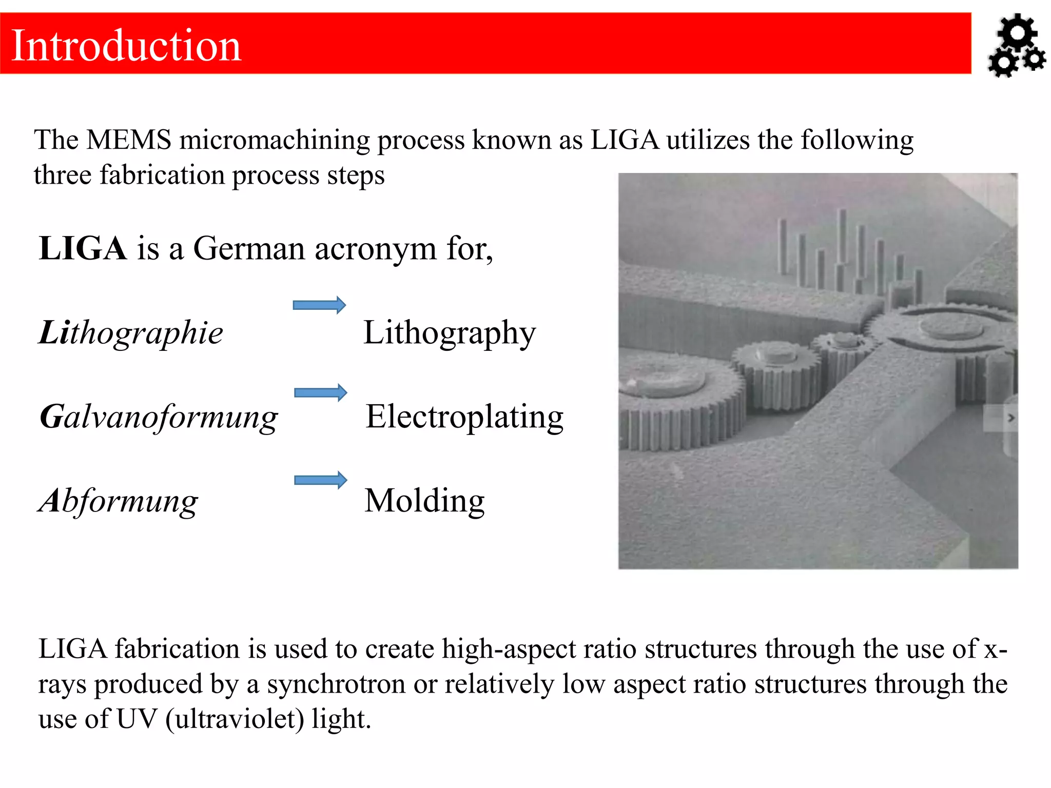

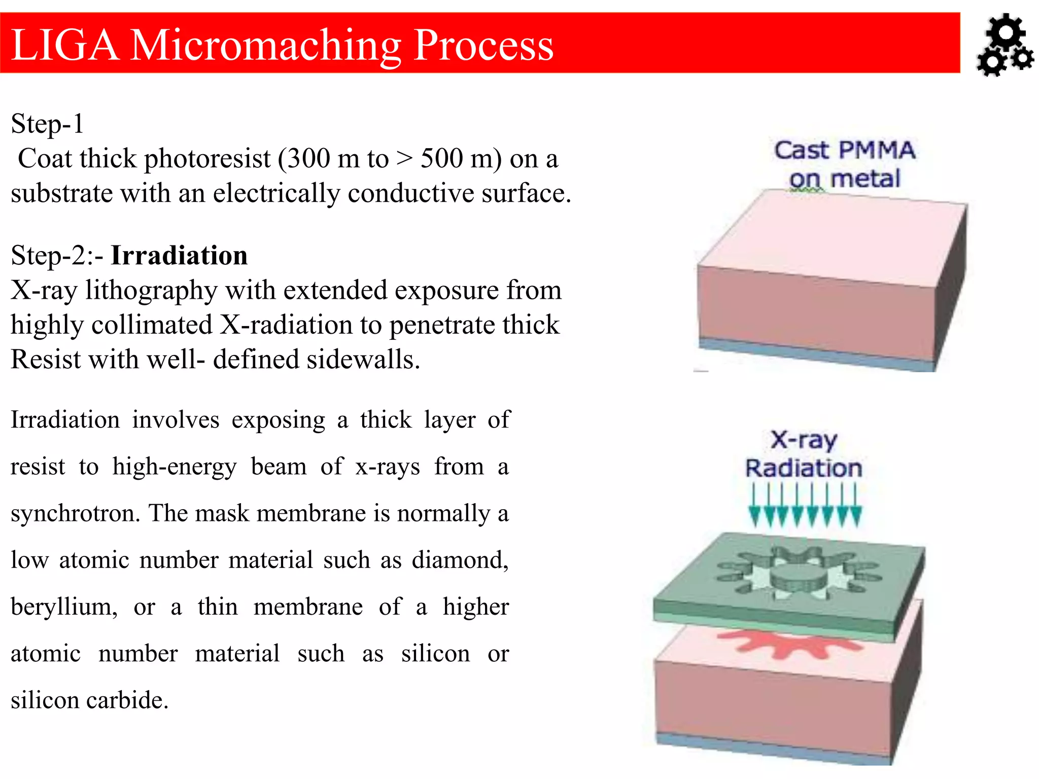
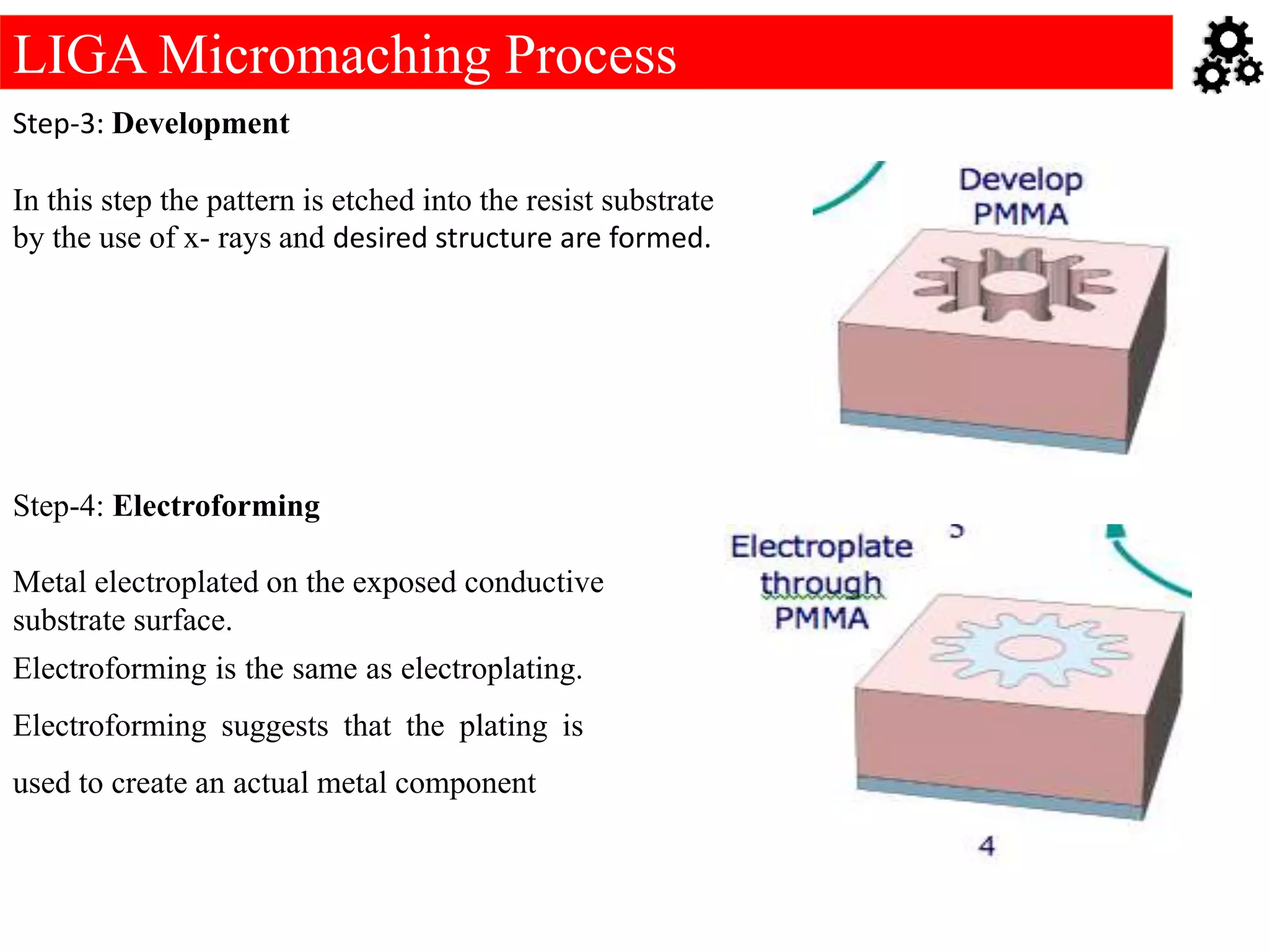
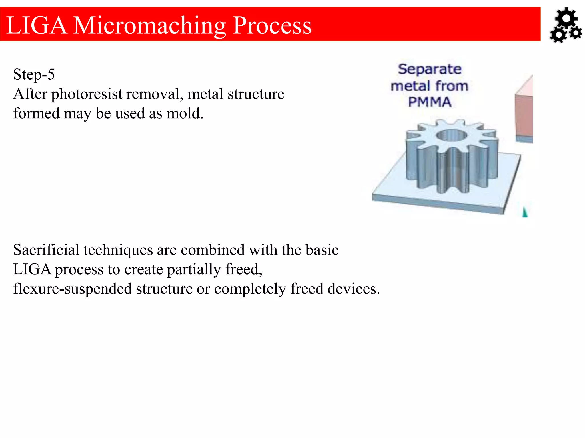
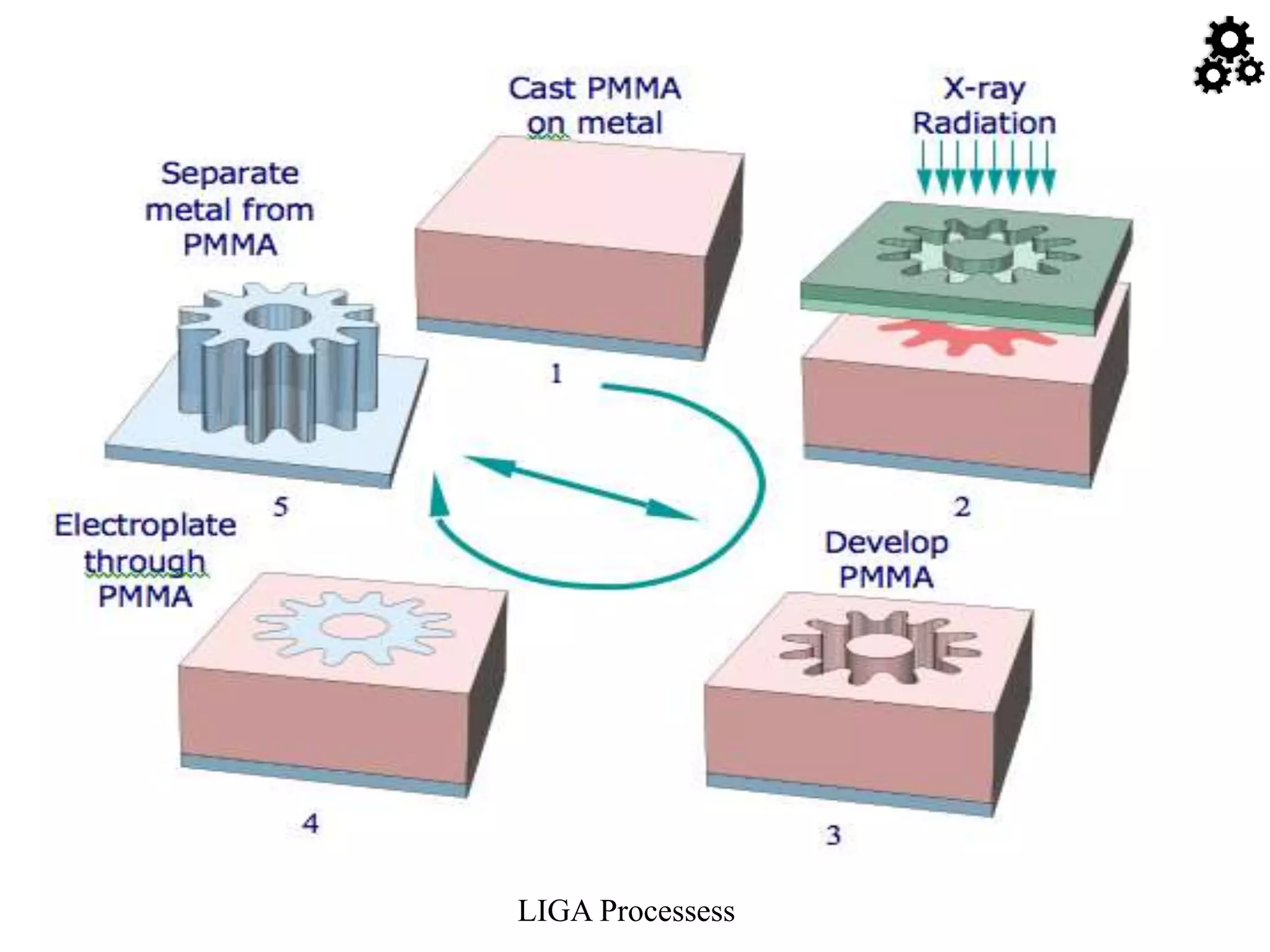
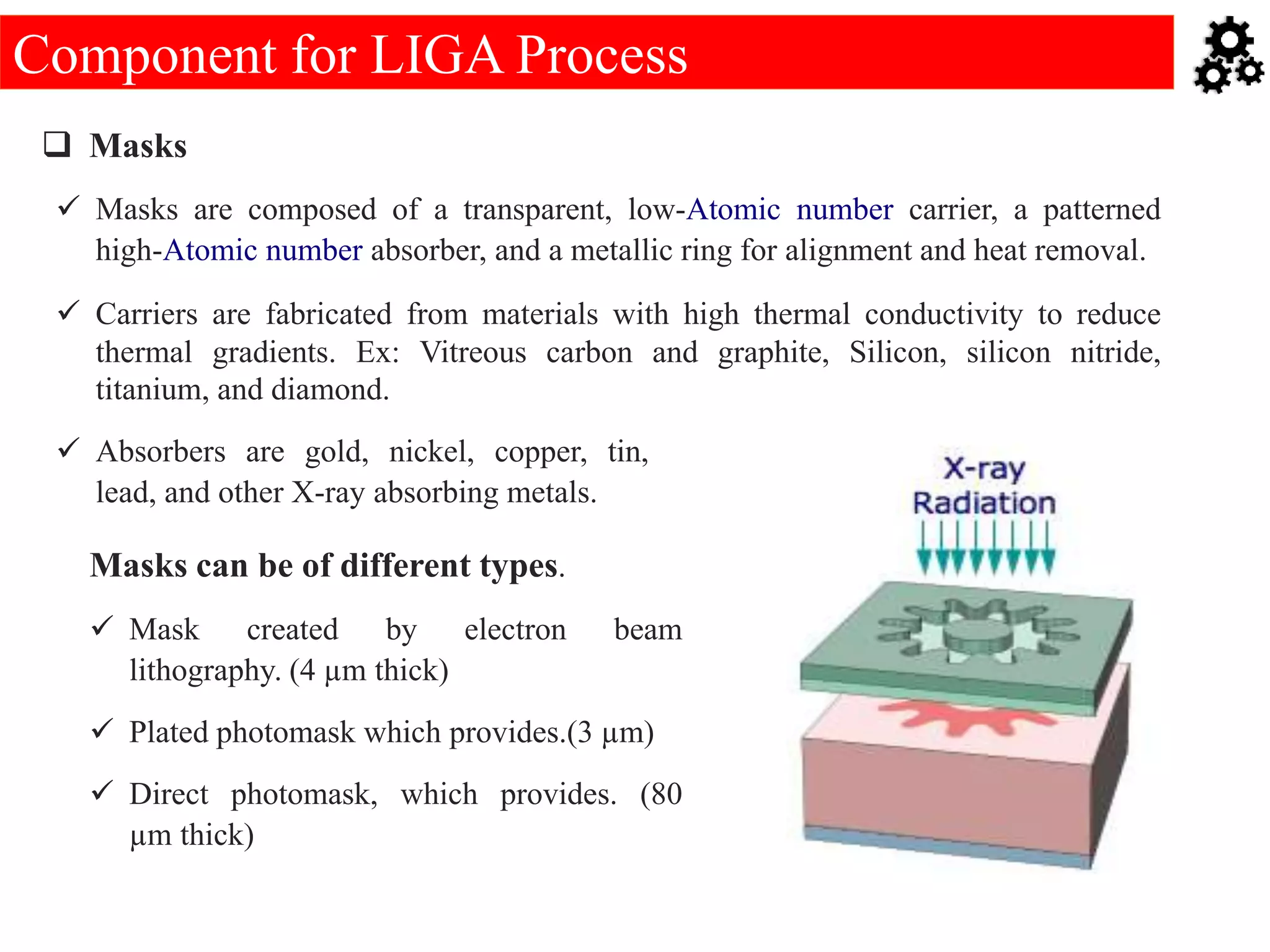


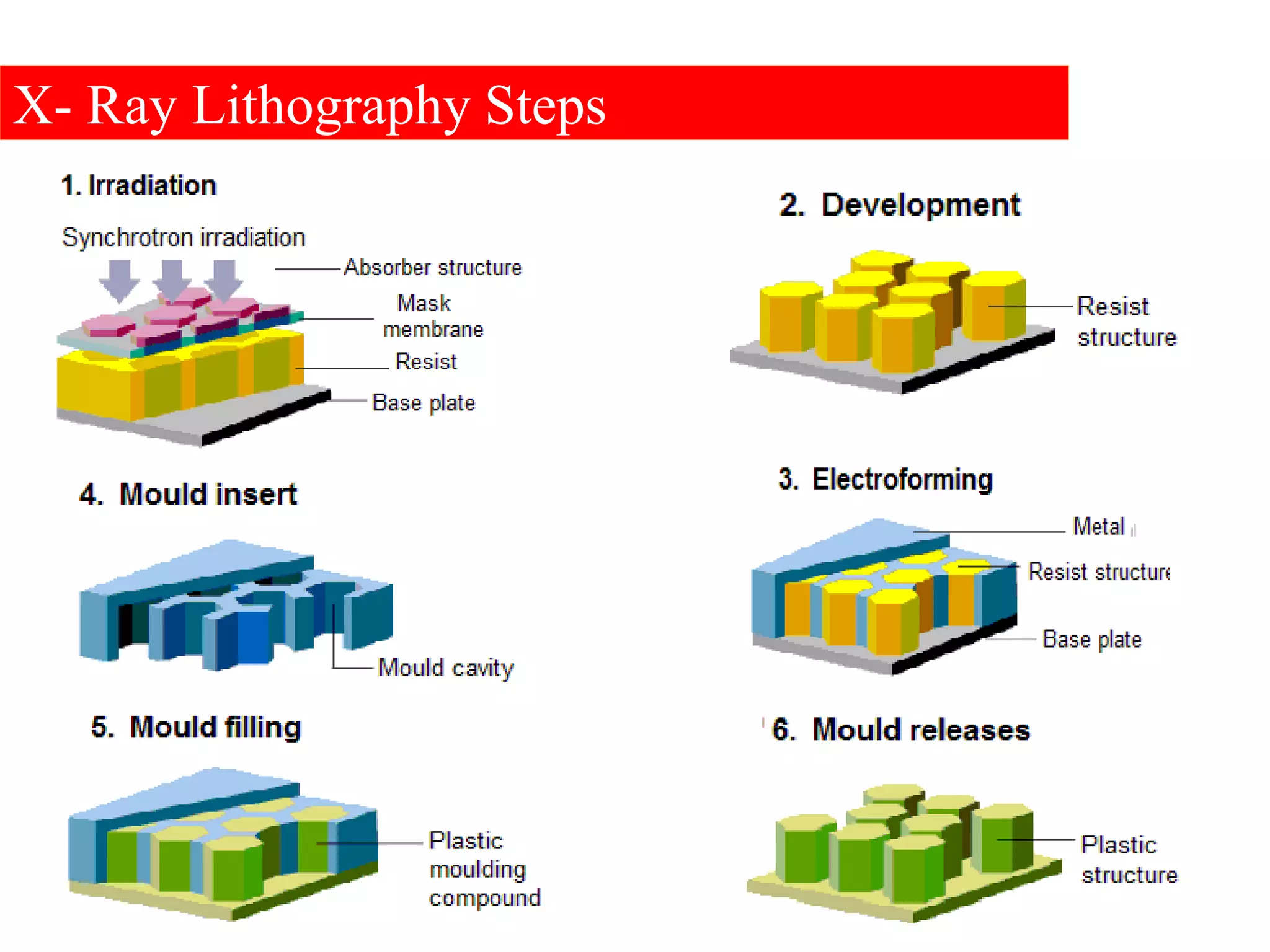


The document describes the LIGA process for fabricating microdevices. It involves three main steps: (1) X-ray lithography to pattern thick photoresist layers, (2) electroplating of metal into the pattern, and (3) removal of the photoresist template to produce free-standing metal microstructures. Key aspects of the LIGA process include using synchrotron radiation for X-ray exposure due to its high intensity and tunability, as well as the ability to create high-aspect-ratio microstructures through thick-resist exposure and development.