Micro electro mechanical systems (MEMS) integrate electrical and mechanical components on a chip, allowing for tiny devices that can sense and control environmental conditions. The fabrication process involves techniques like deposition, patterning, and etching, and MEMS offer advantages such as smaller size, lower power consumption, and system integration. Applications of MEMS span various fields, including automotive, healthcare, and telecommunications, although they can be costly to develop and manufacture.
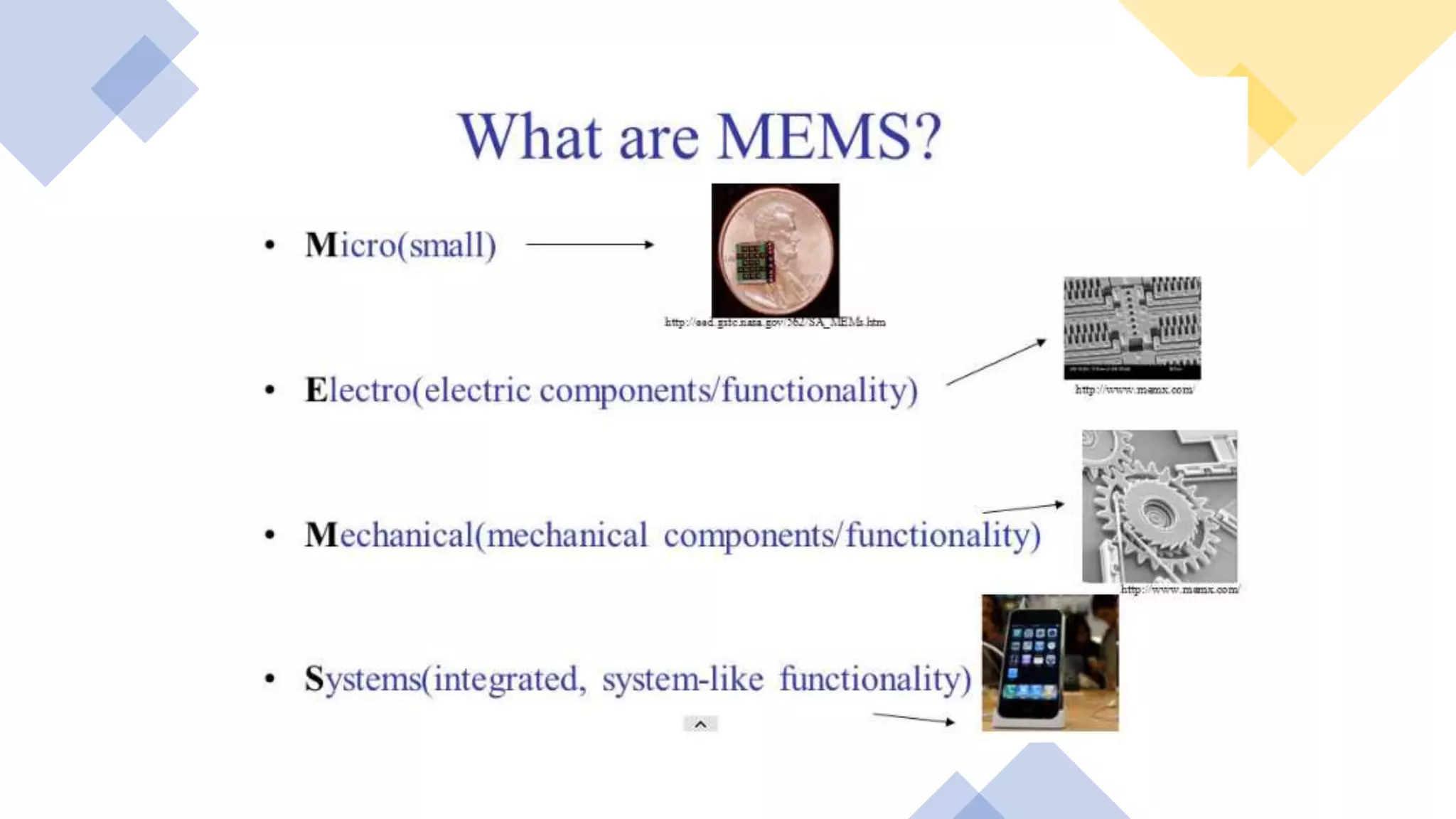
What is MEMS
•Micro electro mechanical system is a technique of combining electrical and mechanical combinations
together on a chip, to produce a system of miniature dimensions.
• MEMS is a integration of a number micro components on a single chip which allow the microsystem
to both sense and control the environment.
• The components are integrated on a single chip using micro fabrication technologies.
5.
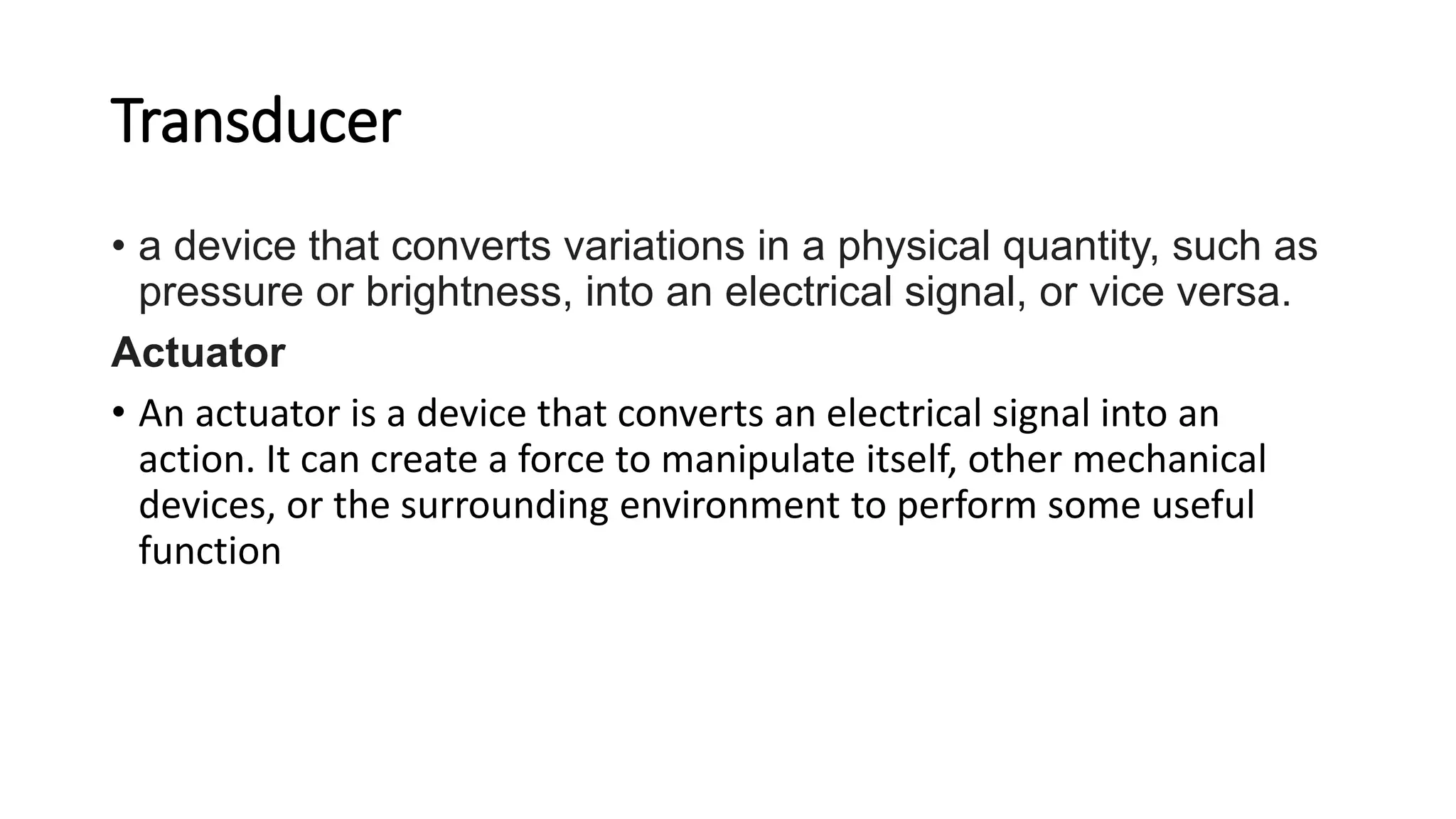
Transducer
• a devicethat converts variations in a physical quantity, such as
pressure or brightness, into an electrical signal, or vice versa.
Actuator
• An actuator is a device that converts an electrical signal into an
action. It can create a force to manipulate itself, other mechanical
devices, or the surrounding environment to perform some useful
function
6.
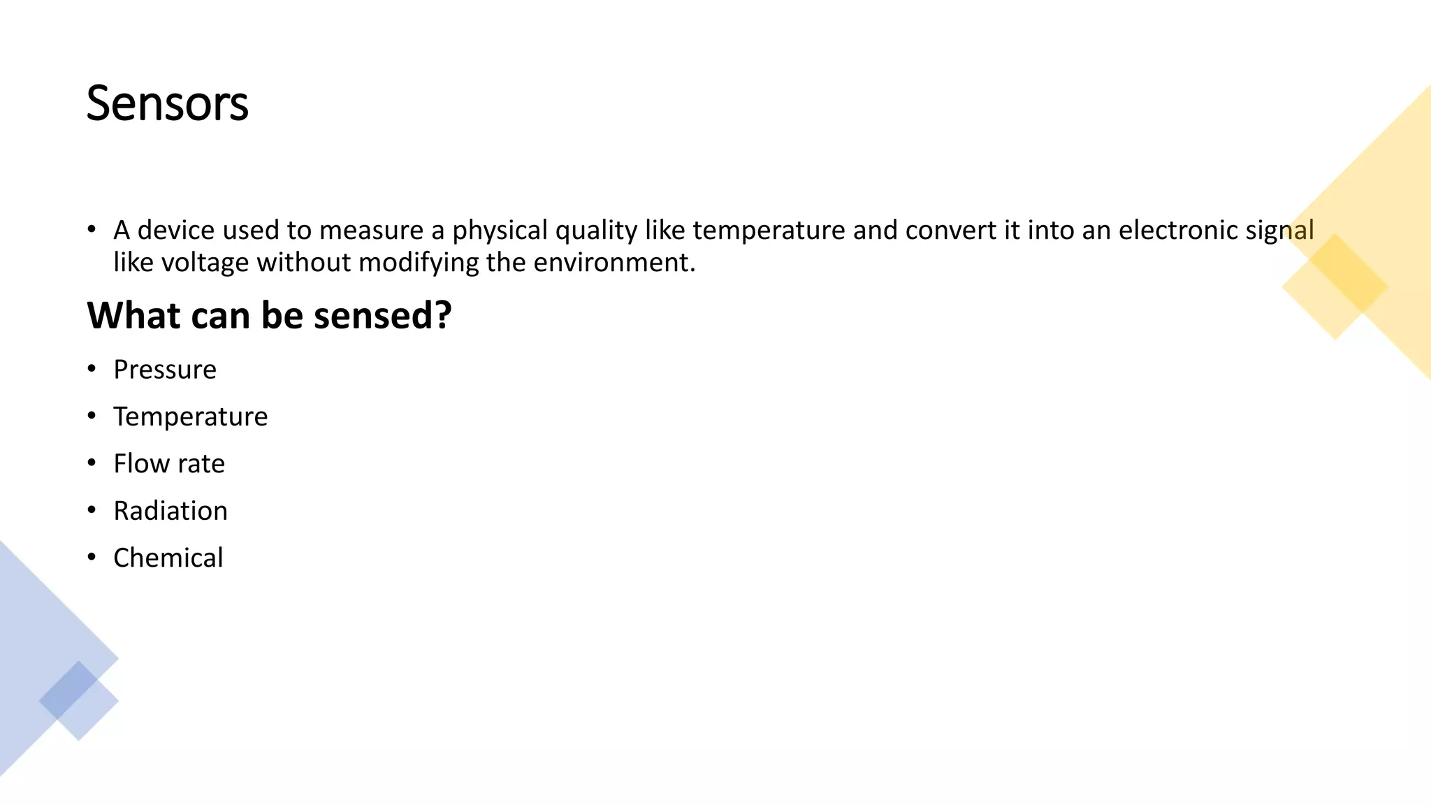
Sensors
• A deviceused to measure a physical quality like temperature and convert it into an electronic signal
like voltage without modifying the environment.
What can be sensed?
• Pressure
• Temperature
• Flow rate
• Radiation
• Chemical
7.
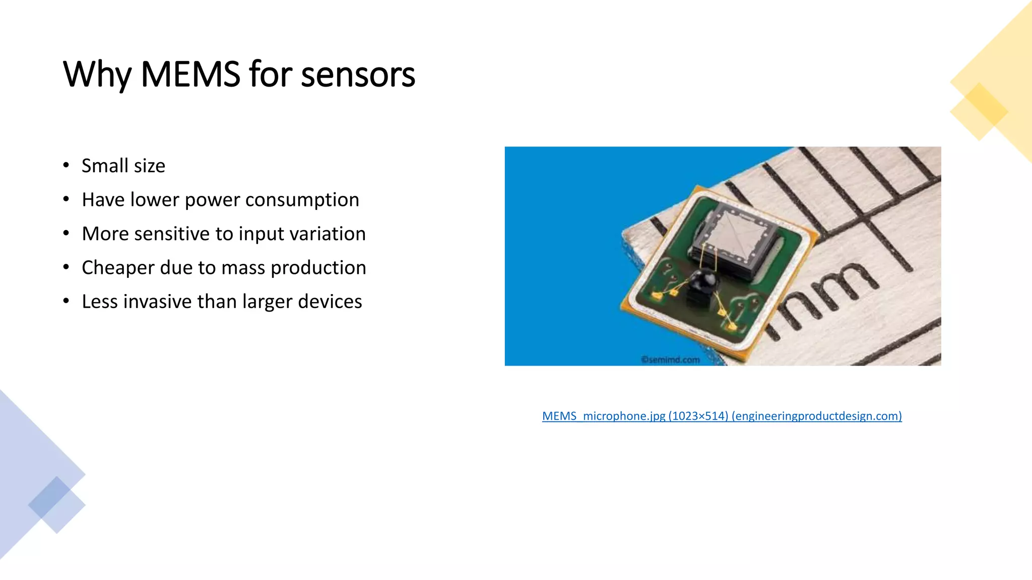
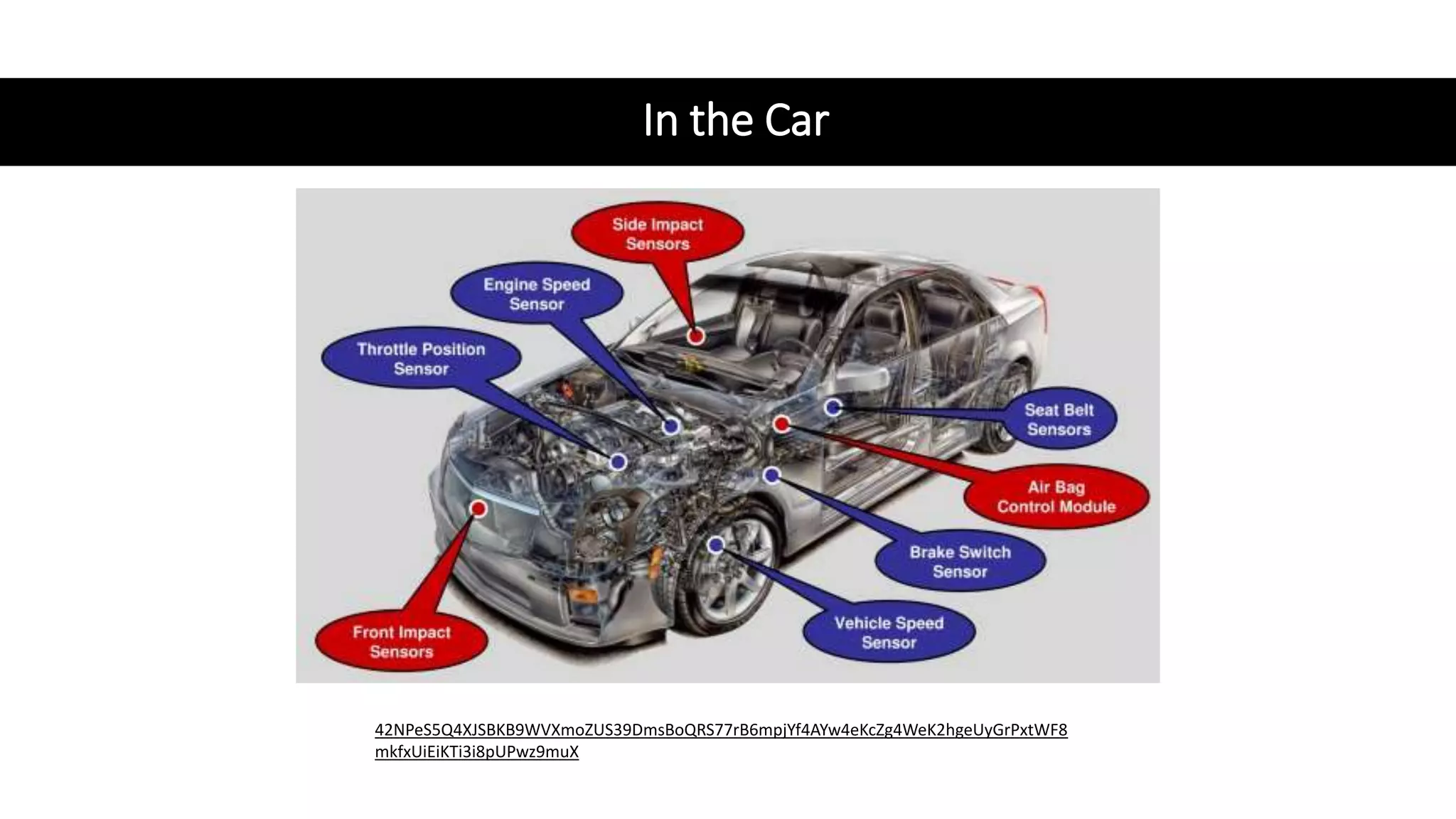
Why MEMS forsensors
• Small size
• Have lower power consumption
• More sensitive to input variation
• Cheaper due to mass production
• Less invasive than larger devices
MEMS_microphone.jpg (1023×514) (engineeringproductdesign.com)
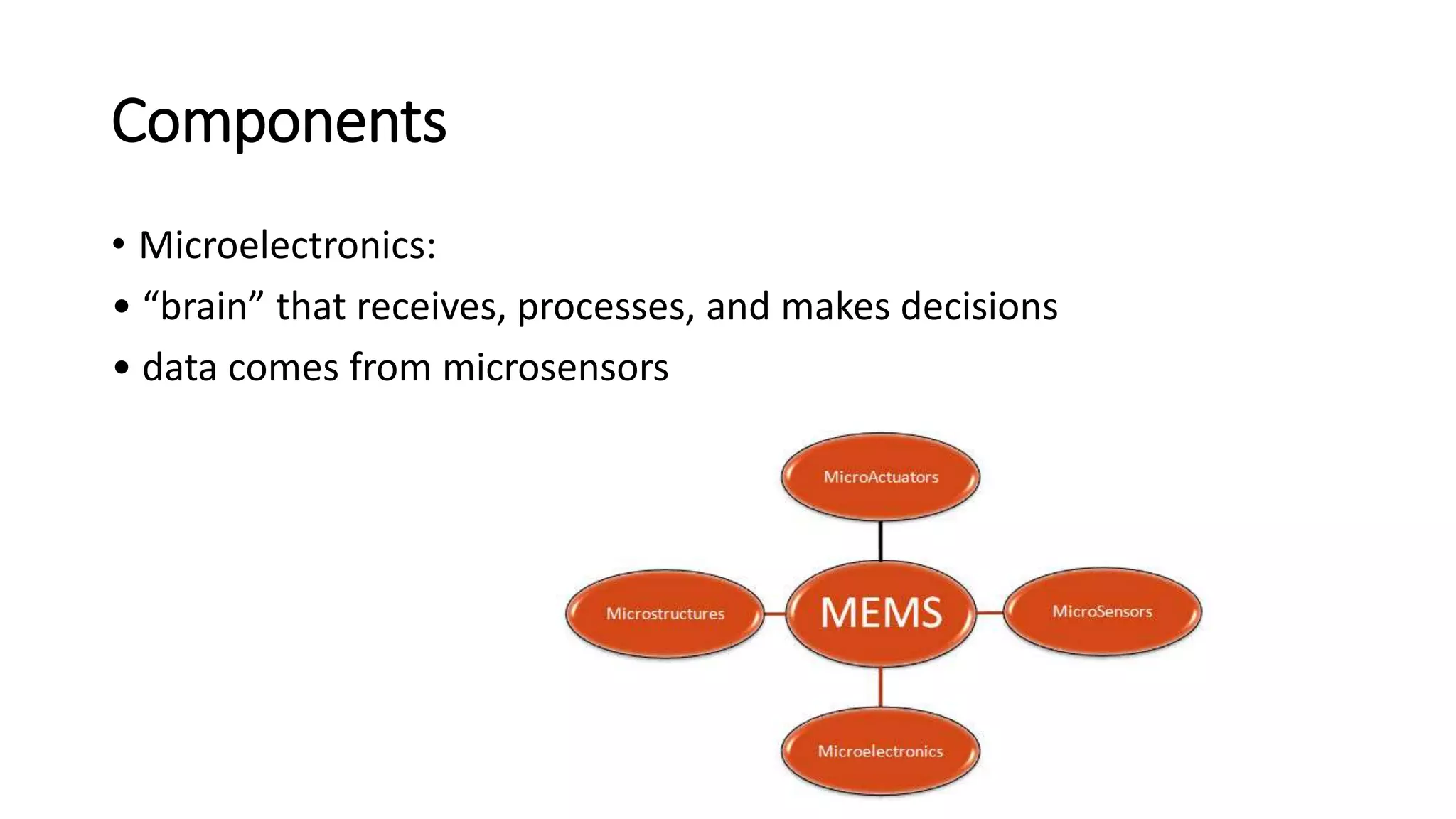
Micro actuator:
• actsas trigger to activate external device
• microelectronics will tell micro actuator to activate
device
Microstructures:
• extremely small structures built onto surface of chip
• built right into silicon of MEMS
Microsensors:
• constantly gather data from environment
• pass data to microelectronics for processing
• can monitor mechanical, thermal, biological, chemical
optical, and magnetic readings
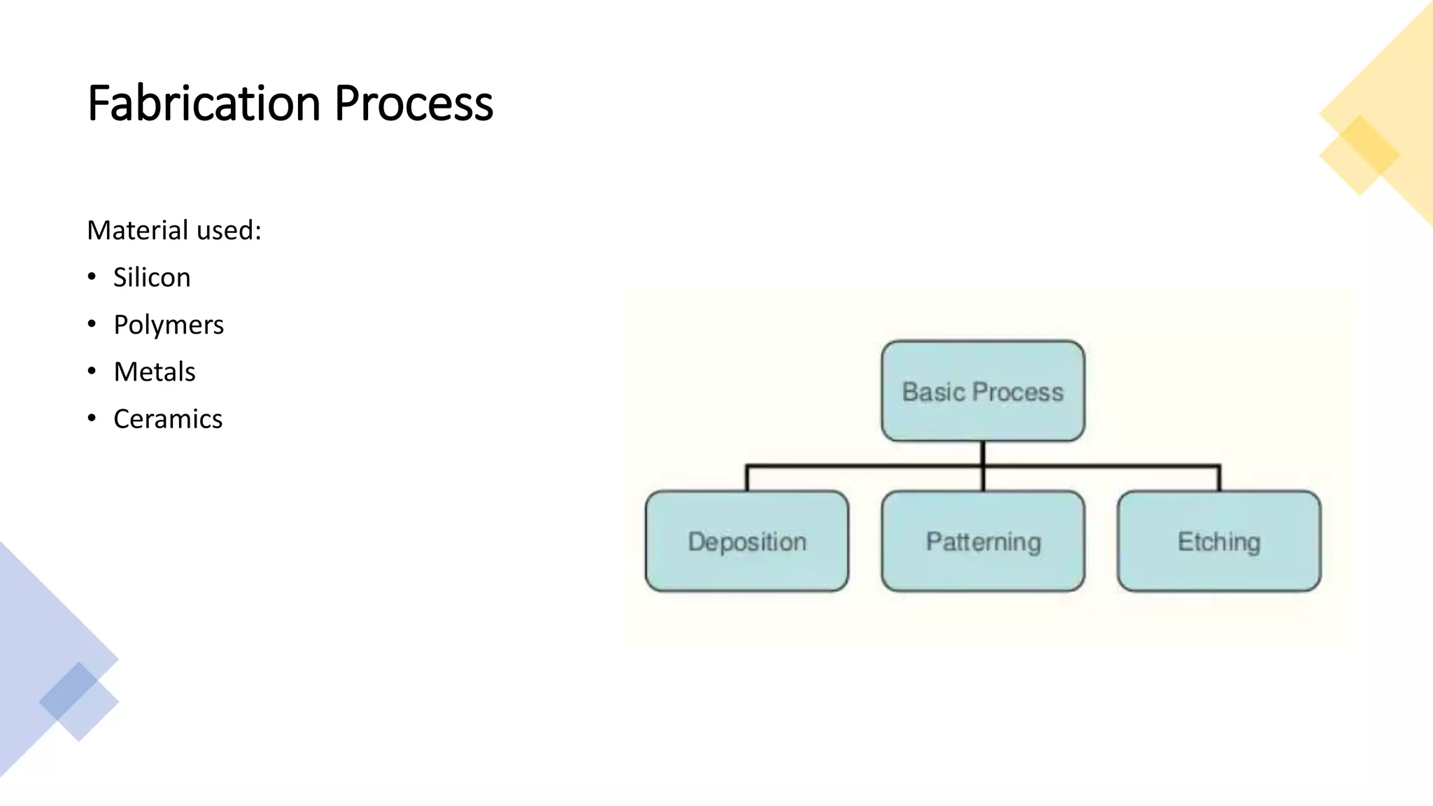
Basic process offabrication
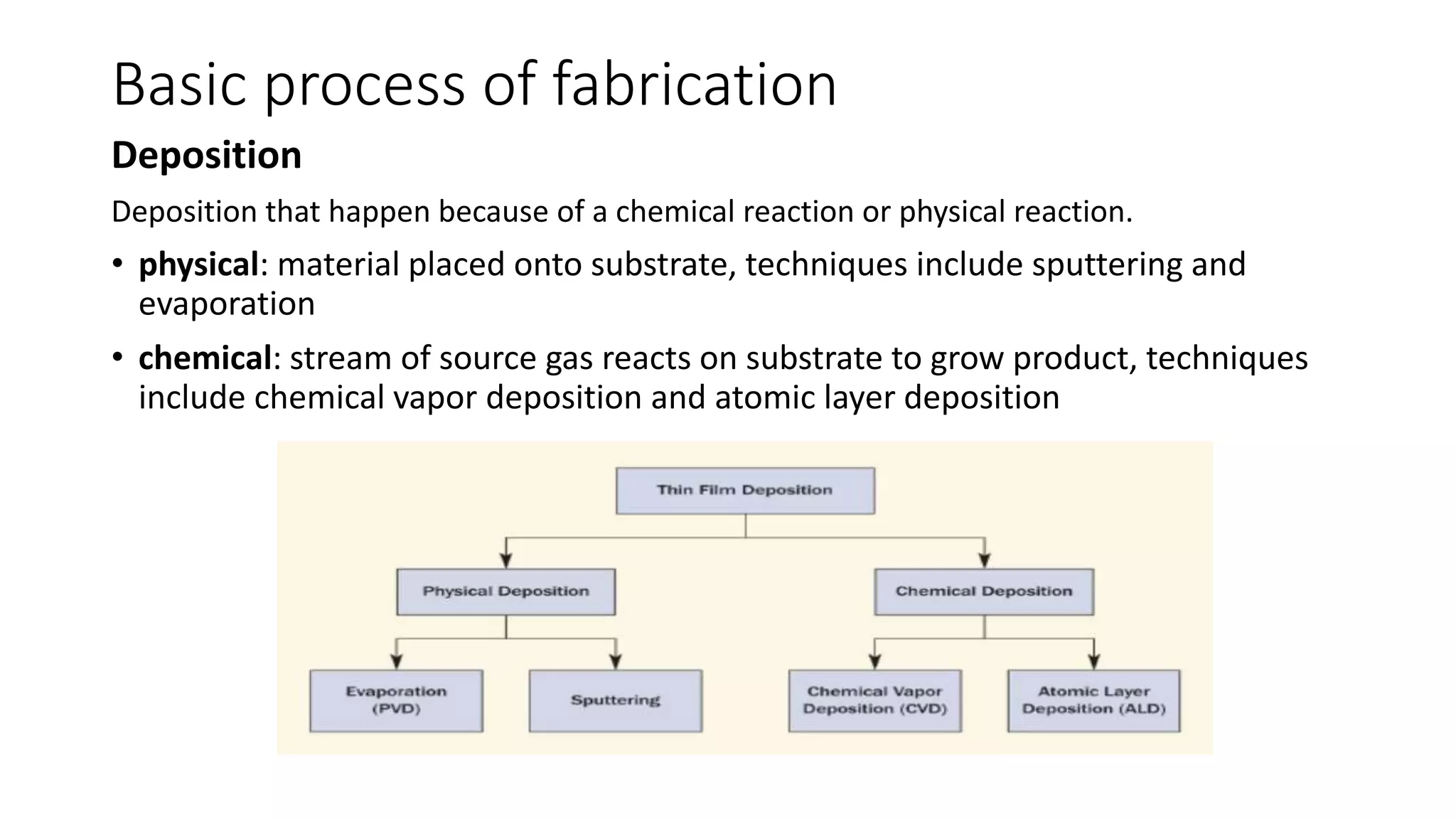
Deposition
Deposition that happen because of a chemical reaction or physical reaction.
• physical: material placed onto substrate, techniques include sputtering and
evaporation
• chemical: stream of source gas reacts on substrate to grow product, techniques
include chemical vapor deposition and atomic layer deposition
12.
• Patterning
The patternis to transfer to a photosensitive material by selective exposure to a radiation source such
as light. If the resist is placed in a developer solution after selective exposure to a light source.
• Etching
It is a process of strong acid to cut into the unprotected parts of a metal surface to create a design.
There are two types:
• Wet etching
• Dey etching
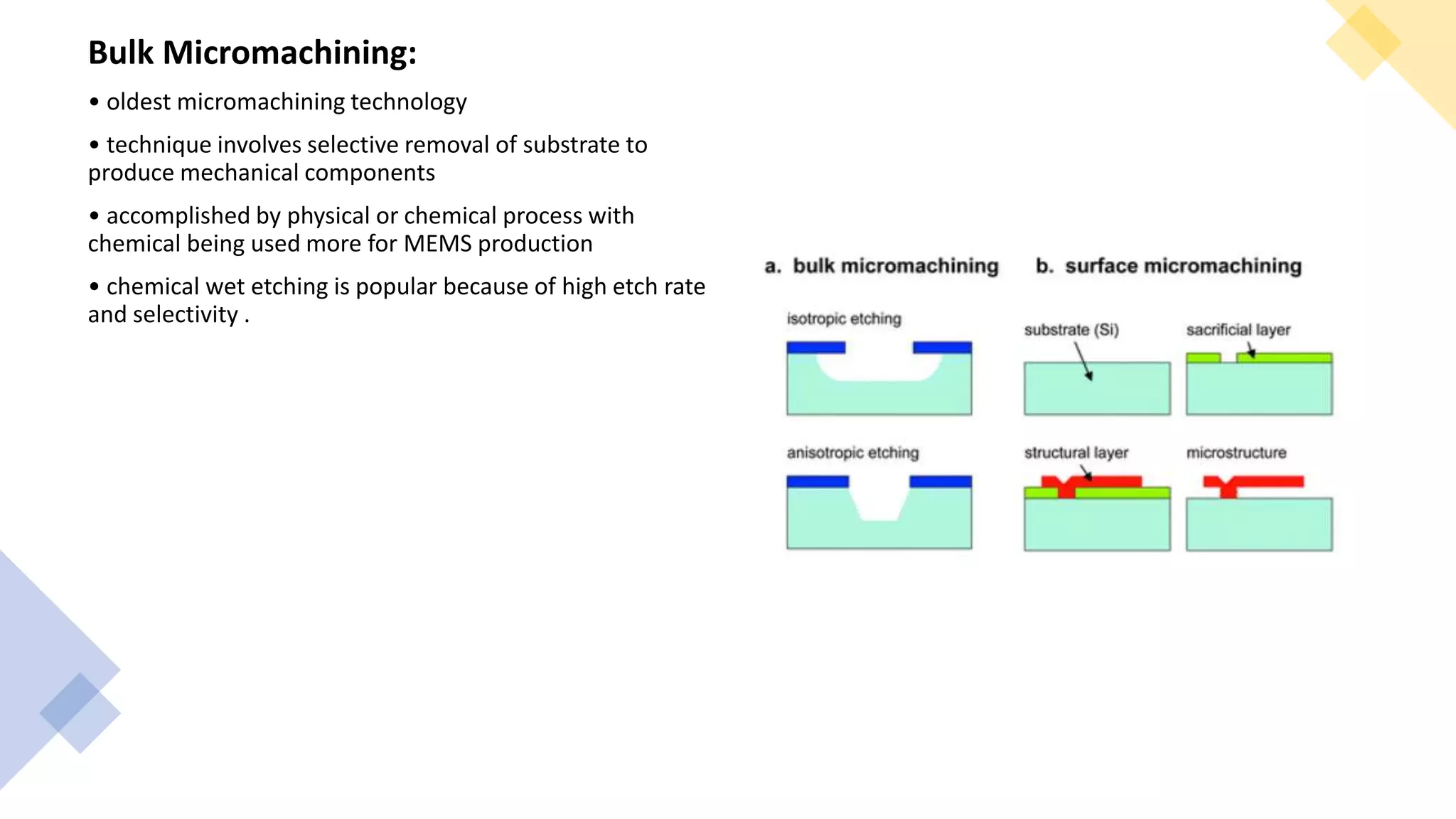
Bulk Micromachining:
• oldestmicromachining technology
• technique involves selective removal of substrate to
produce mechanical components
• accomplished by physical or chemical process with
chemical being used more for MEMS production
• chemical wet etching is popular because of high etch rate
and selectivity .
15.
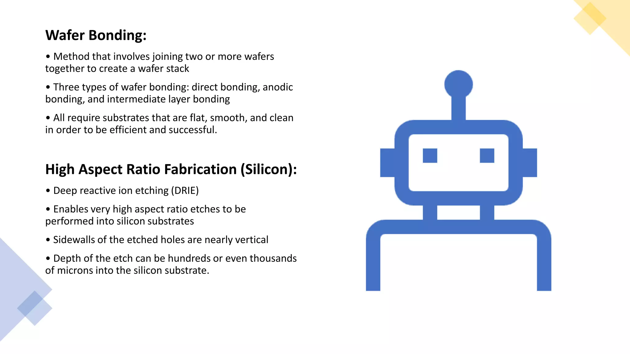
Wafer Bonding:
• Methodthat involves joining two or more wafers
together to create a wafer stack
• Three types of wafer bonding: direct bonding, anodic
bonding, and intermediate layer bonding
• All require substrates that are flat, smooth, and clean
in order to be efficient and successful.
High Aspect Ratio Fabrication (Silicon):
• Deep reactive ion etching (DRIE)
• Enables very high aspect ratio etches to be
performed into silicon substrates
• Sidewalls of the etched holes are nearly vertical
• Depth of the etch can be hundreds or even thousands
of microns into the silicon substrate.
16.
Advantages of MEMS
•Much smaller area
• Cheaper than alternatives
○ In medical market, that means disposable
• Can be integrated with electronics (system on one chip)
• Speed:
○ Lower thermal time constant
○ Rapid response times(high frequency)
• Power consumption:
○ low actuation energy
○ low heating power
17.
Disadvantages of MEMS
•Very expensive during the research and development stage for any new MEMS design or devices
• Very expensive upfront setup cost for fabrication cleanrooms and foundry facilities
• Fabrication and assembly unit costs can be very high for low quantities. Therefore, MEMS are not suitable for
niche applications, unless cost is not an issue
• Testing equipment to characterise the quality and performance can also be expensive
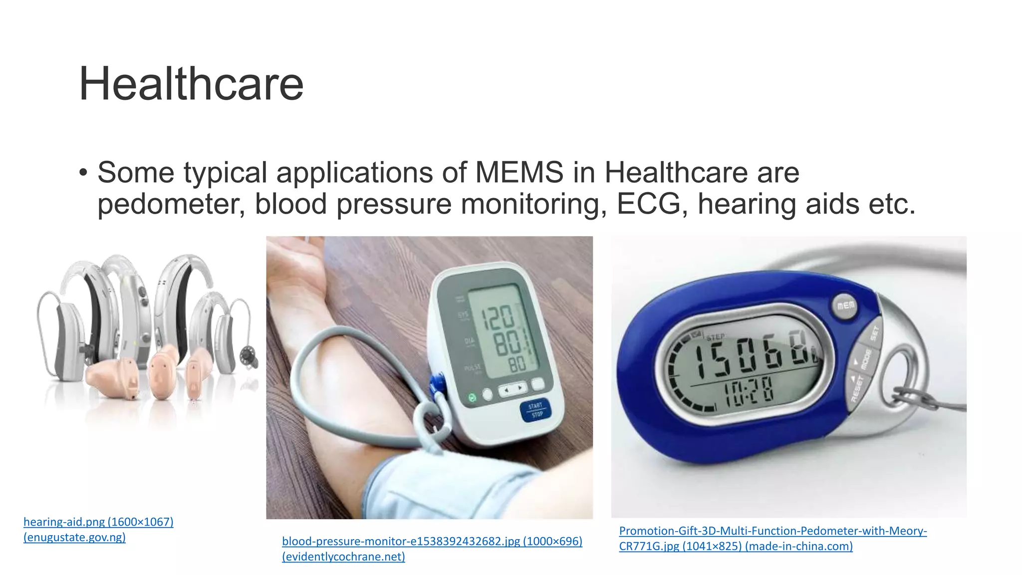
Healthcare
• Some typicalapplications of MEMS in Healthcare are
pedometer, blood pressure monitoring, ECG, hearing aids etc.
blood-pressure-monitor-e1538392432682.jpg (1000×696)
(evidentlycochrane.net)
Promotion-Gift-3D-Multi-Function-Pedometer-with-Meory-
CR771G.jpg (1041×825) (made-in-china.com)
hearing-aid.png (1600×1067)
(enugustate.gov.ng)
21.
Conclusion
• Micro-Electro-Mechanical Systemsare 1-100 micrometer devices that convert electrical energy to
mechanical energy and vice-versa. The three basic steps to MEMS fabrication are deposition,
patterning, and etching. Due to their small size, they can exhibit certain characteristics that their
macro equivalents can’t. MEMS produce benefits in speed, complexity, power consumption, device
area, and system integration. These benefits make MEMS a great choice for devices in numerous
fields.