Download as PDF, PPTX


![Definitions: “Acceptance”: Action by which the Buyer accepts
the terms and conditions of sale in their entirety. It is done by
signing the purchase order which mentions “I hereby accept
Yole’s Terms and Conditions of Sale”.
“Buyer”: Any business user (i.e. any person acting in the course
of its business activities, for its business needs) entering into the
following general conditions to the exclusion of consumers acting
in their personal interests.
“Contracting Parties” or “Parties”: The Seller on the
one hand and the Buyer on the other hand.
“Intellectual Property Rights” (“IPR”) means any
rights held by the Seller in its Products, including any patents,
trademarks, registered models, designs, copyrights, inventions,
commercial secrets and know-how, technical information,
company or trading names and any other intellectual property
rights or similar in any part of the world, notwithstanding the fact
that they have been registered or not and including any pending
registration of one of the above mentioned rights.
“License”: For the reports and databases, 3 different licenses
are proposed. The buyer has to choose one license:
• One user license: one person at the company can use the report.
• Multi-user license: the report can be used by unlimited users
within the company. Subsidiaries and Joint-Ventures are not
included.
• Corporate license: purchased under “Annual Subscription”
program, the report can be used by unlimited users within the
company. Joint-Ventures are not included.
“Products”: Depending on the purchase order, reports or
database on MEMS, CSC, Optics/MOEMS, Nano, bio… to
be bought either on a unit basis or as an annual subscription.
(i.e. subscription for a period of 12 calendar months). The
annual subscription to a package (i.e. a global discount based
on the number of reports that the Buyer orders or accesses
via the service, a global search service on line on I-micronews
and a consulting approach), is defined in the order. Reports are
established in PowerPoint and delivered on a PDF format and the
database may include Excel files.
“Seller”: Based in Lyon (France headquarters), Yole
Développement is a market research and business development
consultancy company, facilitating market access for advanced
technology industrial projects. With more than 20 market
analysts, Yole works worldwide with the key industrial companies,
RD institutes and investors to help them understand the markets
and technology trends.
1. SCOPE
1.1 The Contracting Parties undertake to observe the following
general conditions when agreed by the Buyer and the Seller.
ANY ADDITIONAL, DIFFERENT, OR CONFLICTING
TERMS AND CONDITIONS IN ANY OTHER DOCUMENTS
ISSUED BY THE BUYER AT ANY TIME ARE HEREBY
OBJECTED TO BY THE SELLER, SHALL BE WHOLLY
INAPPLICABLE TO ANY SALE MADE HEREUNDER AND
SHALL NOT BE BINDING IN ANY WAY ON THE SELLER.
1.2 This agreement becomes valid and enforceable between the
Contracting Parties after clear and non-equivocal consent
by any duly authorized person representing the Buyer. For
these purposes, the Buyer accepts these conditions of sales
when signing the purchase order which mentions “I hereby
accept Yole’s Terms and Conditions of Sale”. This results in
acceptance by the Buyer.
1.3 Orders are deemed to be accepted only upon written
acceptance and confirmation by the Seller, within [7 days] from
the date of order, to be sent either by email or to the Buyer’s
address. In the absence of any confirmation in writing, orders
shall be deemed to have been accepted.
2. MAILING OF THE PRODUCTS
2.1 Products are sent by email to the Buyer:
• within [1]
month from the order for Products already
released; or
• within a reasonable time for Products ordered prior to
their effective release. In this case, the Seller shall use its best
endeavours to inform the Buyer of an indicative release date
and the evolution of the work in progress.
2.2 Some weeks prior to the release date the Seller can propose
a pre-release discount to the Buyer
The Seller shall by no means be responsible for any delay in
respect of article 2.2 above, and including incases where a
new event or access to new contradictory information would
require for the analyst extra time to compute or compare
the data in order to enable the Seller to deliver a high quality
Products.
2.3 The mailing of the Product will occur only upon payment
by the Buyer, in accordance with the conditions contained
in article 3.
2.4. The mailing is operated through electronic means either by
email via the sales department or automatically online via an
email/password. If the Product’s electronic delivery format
is defective, the Seller undertakes to replace it at no charge
to the Buyer provided that it is informed of the defective
formatting within 90 days from the date of the original
download or receipt of the Product.
2.5 The person receiving the Products on behalf of the Buyer
shall immediately verify the quality of the Products and their
conformity to the order. Any claim for apparent defects or
for non-conformity shall be sent in writing to the Seller within
8 days of receipt of the Products. For this purpose, the Buyer
agrees to produce sufficient evidence of such defects. .
2.6 No return of Products shall be accepted without prior
information to the Seller, even in case of delayed delivery.
Any Product returned to the Seller without providing prior
information to the Seller as required under article 2.5 shall
remain at the Buyer’s risk.
3. PRICE, INVOICING AND PAYMENT
3.1 Prices are given in the orders corresponding to each Product
sold on a unit basis or corresponding to annual subscriptions.
They are expressed to be inclusive of all taxes. The prices
may be reevaluated from time to time. The effective price is
deemed to be the one applicable at the time of the order.
3.2 Yole may offer a pre release discount for the companies willing
to acquire in the future the specific report and agreeing on the
fact that the report may be release later than the anticipated
release date. In exchange to this uncertainty, the company will
get a discount that can vary from 15% to 10%.
3.3 Payments due by the Buyer shall be sent by cheque payable to
Yole Développement, credit card or by electronic transfer to
the following account:
HSBC, 1 place de la Bourse 69002 Lyon France
Bank code: 30056
Branch code: 00170
Account n°: 0170 200 1565 87
BIC or SWIFT code: CCFRFRPP
IBAN: FR76 3005 6001 7001 7020 0156 587
To ensure the payments, the Seller reserves the right to request
down payments from the Buyer. In this case, the need of down
payments will be mentioned on the order.
3.4 Payment is due by the Buyer to the Seller within 30 days
from invoice date, except in the case of a particular written
agreement. If the Buyer fails to pay within this time and fails
to contact the Seller, the latter shall be entitled to invoice
interest in arrears based on the annual rate Refi of the «BCE»
+ 7 points, in accordance with article L. 441-6 of the French
Commercial Code. Our publications (report, database, tool...)
are delivered only after reception of the payment.
3.5 In the event of termination of the contract, or of misconduct,
during the contract, the Seller will have the right to invoice
at the stage in progress, and to take legal action for damages.
4. LIABILITIES
4.1 The Buyer or any other individual or legal person acting on
its behalf, being a business user buying the Products for its
business activities, shall be solely responsible for choosing the
Products and for the use and interpretations he makes of the
documents it purchases, of the results he obtains, and of the
advice and acts it deduces thereof.
4.2 The Seller shall only be liable for (i) direct and (ii) foreseeable
pecuniary loss, caused by the Products or arising from a
material breach of this agreement
4.3 In no event shall the Seller be liable for:
a) damages of any kind, including without limitation, incidental
or consequential damages (including, but not limited to,
damages for loss of profits, business interruption and loss of
programs or information) arising out of the use of or inability
to use the Seller’s website or the Products, or any information
provided on the website, or in the Products;
b) any claim attributable to errors, omissions or other
inaccuracies in the Product or interpretations thereof.
4.4 All the information contained in the Products has been
obtained from sources believed to be reliable. The Seller
does not warrant the accuracy, completeness adequacy or
reliability of such information, which cannot be guaranteed to
be free from errors.
4.5 All the Products that the Seller sells may, upon prior notice
to the Buyer from time to time be modified by or substituted
with similar Products meeting the needs of the Buyer. This
modification shall not lead to the liability of the Seller,
provided that the Seller ensures the substituted Product is
similar to the Product initially ordered.
4.6 In the case where, after inspection, it is acknowledged that
the Products contain defects, the Seller undertakes to replace
the defective products as far as the supplies allow and without
indemnities or compensation of any kind for labor costs,
delays, loss caused or any other reason. The replacement is
guaranteed for a maximum of two months starting from the
delivery date. Any replacement is excluded for any event as set
out in article 5 below.
4.7 The deadlines that the Seller is asked to state for the mailing
of the Products are given for information only and are not
guaranteed. If such deadlines are not met, it shall not lead to
any damages or cancellation of the orders, except for non
acceptable delays exceeding [4] months from the stated
deadline, without information from the Seller. In such case only,
the Buyer shall be entitled to ask for a reimbursement of its first
down payment to the exclusion of any further damages.
4.8 The Seller does not make any warranties, express or implied,
including, without limitation, those of sale ability and fitness for
a particular purpose, with respect to the Products. Although
the Seller shall take reasonable steps to screen Products for
infection of viruses, worms, Trojan horses or other codes
containing contaminating or destructive properties before
making the Products available, the Seller cannot guarantee
that any Product will be free from infection.
5. FORCE MAJEURE
The Seller shall not be liable for any delay in performance directly
or indirectly caused by or resulting from acts of nature, fire, flood,
accident, riot, war, government intervention, embargoes, strikes,
labor difficulties, equipment failure, late deliveries by suppliers or
other difficulties which are beyond the control, and not the fault
of the Seller.
6. PROTECTION OF THE SELLER’S IPR
6.1 All the IPR attached to the Products are and remain the
property of the Seller and are protected under French and
international copyright law and conventions.
6.2 The Buyer agreed not to disclose, copy, reproduce,
redistribute, resell or publish the Product, or any part of it
to any other party other than employees of its company. The
Buyer shall have the right to use the Products solely for its
own internal information purposes. In particular, the Buyer
shall therefore not use the Product for purposes such as:
• Information storage and retrieval systems;
• Recordings and re-transmittals over any network (including
any local area network);
• Use in any timesharing, service bureau, bulletin board or
similar arrangement or public display;
• Posting any Product to any other online service (including
bulletin boards or the Internet);
• Licensing, leasing, selling, offering for sale or assigning the
Product.
6.3 The Buyer shall be solely responsible towards the Seller of
all infringements of this obligation, whether this infringement
comes from its employees or any person to whom the Buyer
has sent the Products and shall personally take care of any
related proceedings, and the Buyer shall bear related financial
consequences in their entirety.
6.4 The Buyer shall define within its company point of contact for
the needs of the contract. This person will be the recipient
of each new report in PDF format. This person shall also be
responsible for respect of the copyrights and will guaranty that
the Products are not disseminated out of the company.
6.5 In the context of annual subscriptions, the person of contact
shall decide who within the Buyer, shall be entitled to access
on line the reports on I-micronews.com. In this respect, the
Seller will give the Buyer a maximum of 10 password, unless
the multiple sites organization of the Buyer requires more
passwords. The Seller reserves the right to check from time
to time the correct use of this password.
6.6 In the case of a multisite, multi license, only the employee
of the buyer can access the report or the employee of the
companies in which the buyer have 100% shares. As a matter
of fact the investor of a company, the joint venture done with
a third party etc..cannot access the report and should pay a
full license price.
7. TERMINATION
7.1 If the Buyer cancels the order in whole or in part or postpones
the date of mailing, the Buyer shall indemnify the Seller for
the entire costs that have been incurred as at the date of
notification by the Buyer of such delay or cancellation. This
may also apply for any other direct or indirect consequential
loss that may be borne by the Seller, following this decision.
7.2 In the event of breach by one Party under these conditions
or the order, the non-breaching Party may send a notification
to the other by recorded delivery letter upon which, after a
period of thirty (30) days without solving the problem, the
non-breaching Party shall be entitled to terminate all the
pending orders, without being liable for any compensation.
8. MISCELLANEOUS
All the provisions of these Terms and Conditions are for the
benefit of the Seller itself, but also for its licensors, employees
and agents. Each of them is entitled to assert and enforce those
provisions against the Buyer.
Any notices under these Terms and Conditions shall be given in
writing. They shall be effective upon receipt by the other Party.
The Seller may, from time to time, update these Terms and
Conditions and the Buyer, is deemed to have accepted the latest
version of these terms and conditions, provided they have been
communicated to him in due time.
9. GOVERNING LAW AND JURISDICTION
9.1 Any dispute arising out or linked to these Terms and
Conditions or to any contract (orders) entered into in
application of these Terms and Conditions shall be settled
by the French Commercial Courts of Lyon, which shall have
exclusive jurisdiction upon such issues.
9.2 French law shall govern the relation between the Buyer and
the Seller, in accordance with these Terms and Conditions.
TERMS AND CONDITIONS OF SALES](https://image.slidesharecdn.com/yolegassensortechnologyandmarketfebruary2016sample-160210150123/75/Gas-Sensor-Technology-and-Market-2016-Report-by-Yole-Developpement-15-2048.jpg)


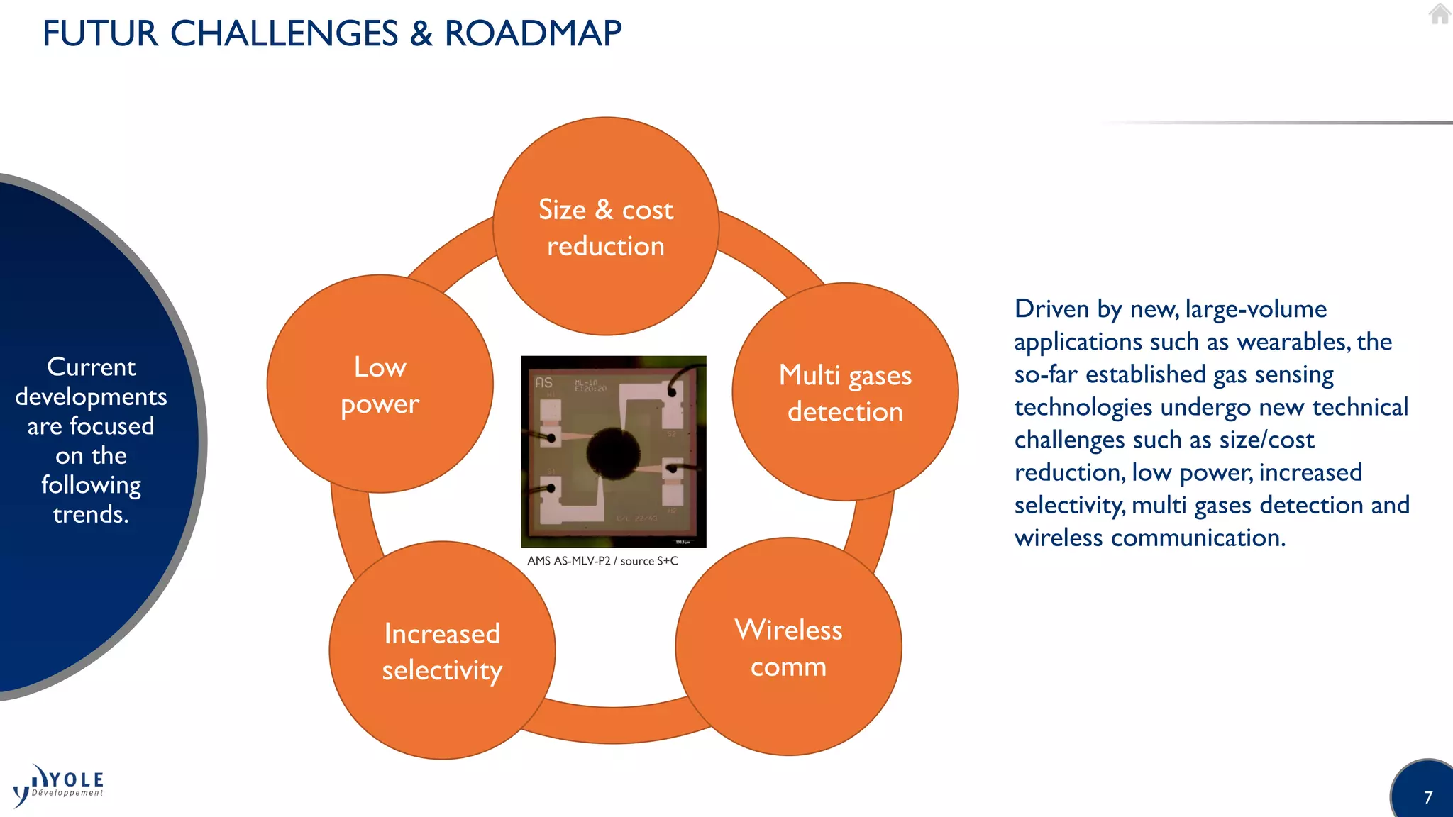
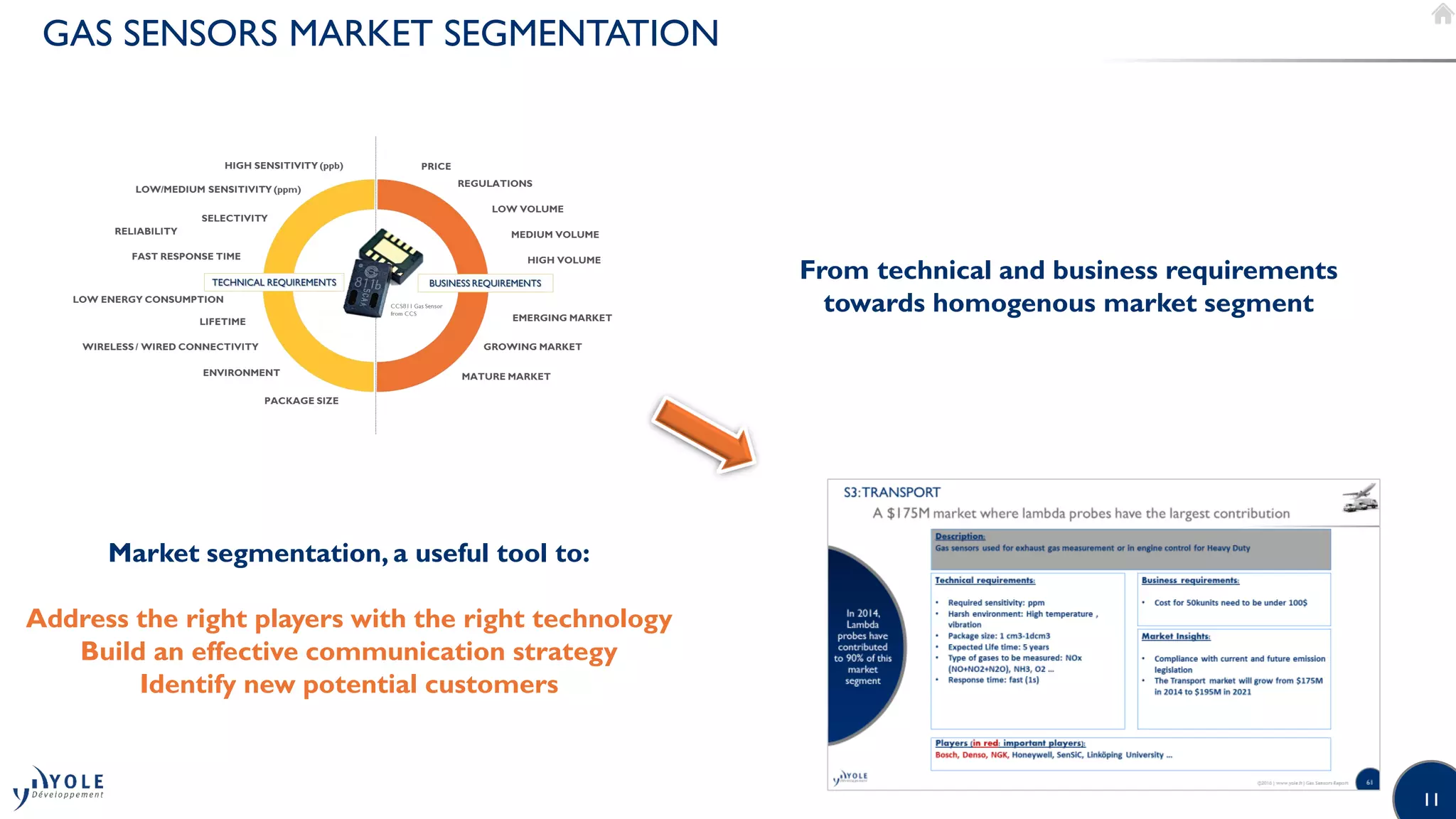
The document is a comprehensive report on gas sensors, covering market analysis, technology trends, and key players in the industry. It includes forecasts for market size and segmentation across various applications such as consumer, medical, and industrial sectors. The document aims to inform companies, investors, and researchers about the evolving landscape of gas sensing technologies and their potential applications.


![Vibe Coding vs. Spec-Driven Development [Free Meetup]](https://cdn.slidesharecdn.com/ss_thumbnails/vibecodingvsspecdrivendevelopment-251209105622-43f455e7-thumbnail.jpg?width=640&height=640&fit=bounds)


