Download to read offline


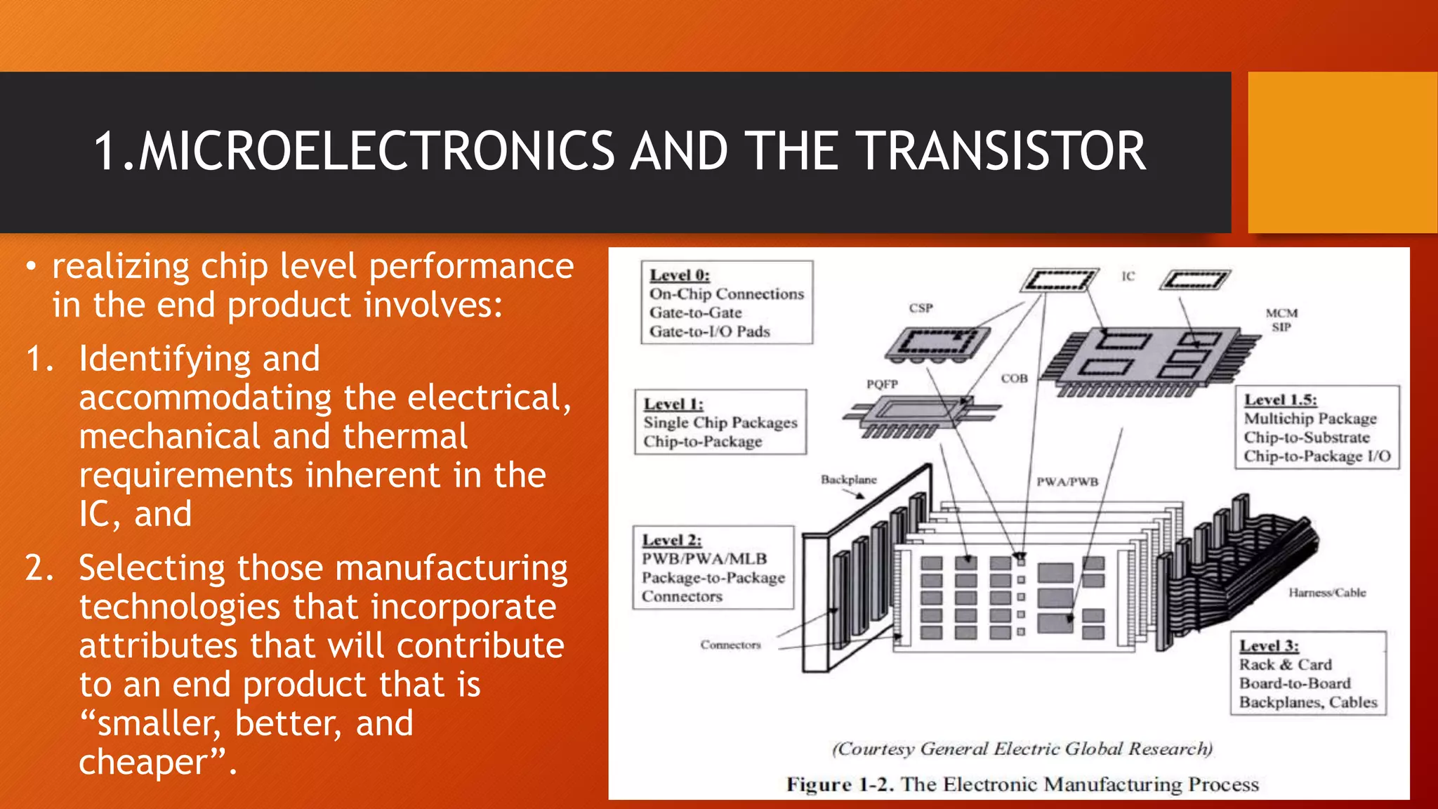


The document discusses the history and development of electronic manufacturing and integrated circuits. It begins with the invention of the transistor in 1947 and its replacement of germanium with silicon. The integrated circuit was developed in 1958, combining multiple transistors on a single silicon chip. Gordon Moore observed that the number of transistors on integrated circuits doubled every year (Moore's Law). Key developments included the microprocessor in 1971 and dynamic random access memory. The document also describes the various levels of interconnection and packaging used to produce electronic devices and circuits.


![ppt on IC [Integrated Circuit]](https://cdn.slidesharecdn.com/ss_thumbnails/1-171227170055-thumbnail.jpg?width=640&height=640&fit=bounds)