Downloaded 157 times
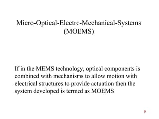

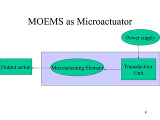


The document presents an overview of Micro-Optical-Electro-Mechanical Systems (MOEMS) and their integration with microelectronic components to create microsensors and actuators. It discusses the manufacturing, design parameters, methodologies, and applications of MOEMS in various fields such as biomedical, automotive, and communication technologies. Additionally, it highlights the benefits of MOEMS, including cost-effectiveness, reliability, and miniaturization.


