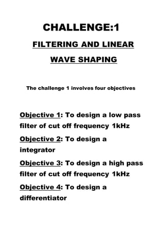
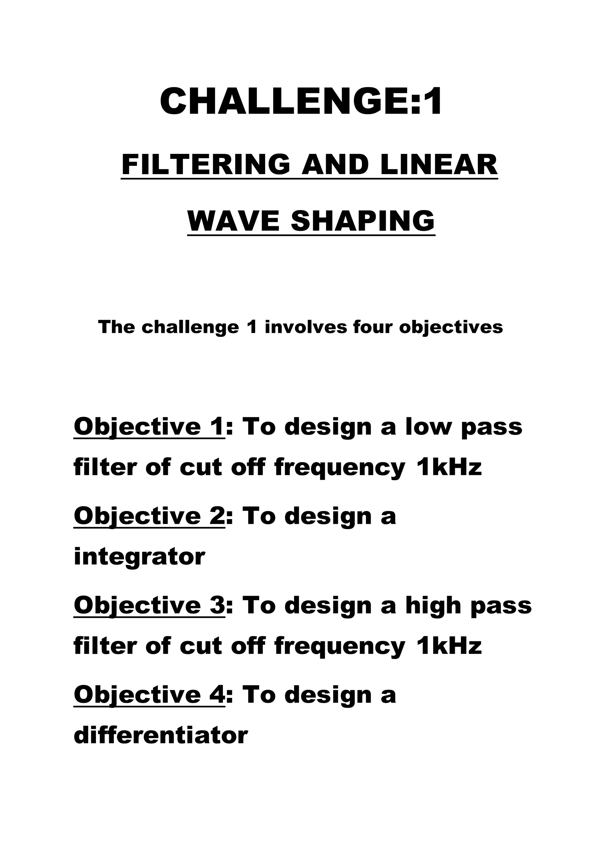
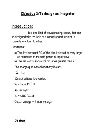
The document discusses the objectives of designing various linear wave shaping circuits including a low pass filter, integrator, high pass filter, and differentiator. It provides details on the design, components, procedure, and results for each objective. For the low pass filter and integrator objectives, it discusses the expected output waveforms for different conditions. The key points are:
1) Objectives are to design four linear wave shaping circuits with cut-off frequencies of 1kHz.
2) Details on the design, components, procedure, and results are provided for a low pass filter and integrator.
3) The behavior of the low pass filter and integrator are studied under different conditions to observe their wave shaping capabilities.
![Assumptions:
Capacitor of value 47nf
If capacitor is in pf range resistaince is in mega
range which is not available in the lab.
If µf range capacitor is taken resistaince is in
ohm but loading effect is high.
So we take capacitor in nf range so that we get resistaince in
kΩ range so that we use it.
Cut off frequency = 1kHz
Resistaince = 1/2πfc =1/2π103*47*10-9 = 3.38kΩ
But in lab we have the standard value of 3.3kΩ in the lab
Vinput = 10v[peak-peak]
C1
47nF
R1
3.3kΩ](https://image.slidesharecdn.com/challenge1-150728123237-lva1-app6891/85/Low-pass-filter-and-Integrator-3-320.jpg)
![Procedure:
a) Verify the circuit design.
b) Set up the circuit as in the design using resistor and
capacitor.
c) Give the input voltage 10v and frequency [varying].
d) Measure and record output voltage according to varying
frequency around the cut off frequency.
e) Determine the gain through the formula gain =
20log[vout/vinp].
f) Plot the graph [x-axis frequency and y-axis output].
Tabular Column
No Frequency
[Hz]
Output
Voltage [V]
Gain [dB]=
20log[vout/vin]
1 100Hz 10 0
2 300Hz 10 0
3 500Hz 10 0
4 600Hz 9 -0.91
5 900Hz 8 -1.93
6 1000Hz 7 -3.09
7 1100Hz 6.2 -4.15](https://image.slidesharecdn.com/challenge1-150728123237-lva1-app6891/85/Low-pass-filter-and-Integrator-4-320.jpg)
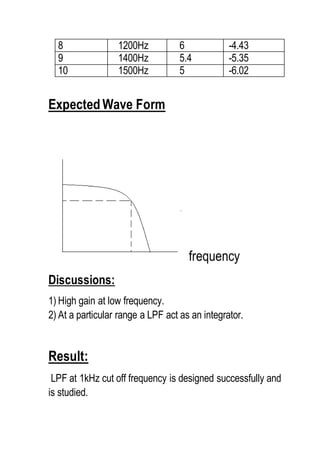
![Low pass filter as an integrator:
Theory:
In low pass circuit, if the time constant is very large in
comparison with the time required for the input signal to make
an appreciable change, the circuit is called an
“integrator”. Under these circumstances the voltage drop
across C will be very small in comparison to the drop across
R and almost the total input Vi appears across R .i.e., i =
Vi/R.
∴The output signal across C is
i.e., the output is proportional to the integral of the
input. Hence the low pass RC circuit acts as a integrator
for RC >> T.
For observing this 3 conditions are to be taken
a) RC = T b) RC>> T c) RC<<T
RC = 3.3*103*47*10-9 = 1.551*10-4
So 1/RC = 6447.45Hz [as 1/T = frequency]
The output waveform is obtained for 3 conditions and it is
plotted on the graph.](https://image.slidesharecdn.com/challenge1-150728123237-lva1-app6891/85/Low-pass-filter-and-Integrator-6-320.jpg)
![Let us assume the frequency = 1kHz
Fc = 1/2πRC
Xc = 1/2πFc = 1/2π*103*47*10-9
So we take resistaince and capacitance value as same in
LPF we designed,
Xc = 3.38kΩ
In an integrator, R>>10Xc so R>>10*3.38kΩ = R>>33.8kΩ
Components Required:
1) Capacitor 47nf 2) resistor 33.8kΩ[33kΩ standard value]
3) CRO 4) function generator 5) bread board
Procedure:
a) Set up the circuit as per the design
R1
33kΩ
C1
47F](https://image.slidesharecdn.com/challenge1-150728123237-lva1-app6891/85/Low-pass-filter-and-Integrator-10-320.jpg)
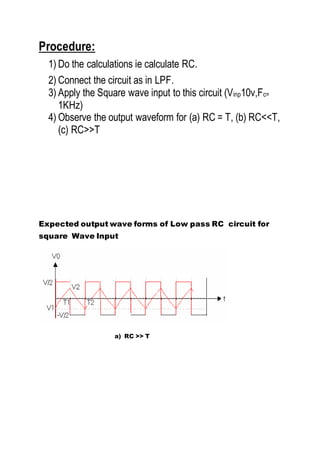
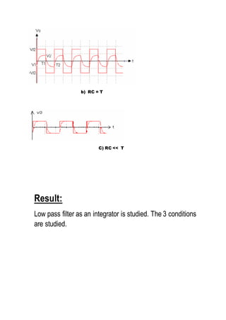
![b) Give a square input of 10V [peak-peak] using a function
generator.
c) Analyse and observe the output on CRO.
d) Sketch obtained graph
Expected Wave form:
Observation:
a) For a square input the result is a triangular wave.
b) For a sin wave input the output is sin wave with a phase
difference.
c) Integrator act as a Low pass filter below / above a
particular frequency which is calculated[Fc].
Result:
Integrator with cut off frequency 1kHz is designed and
the wave form is obtained.](https://image.slidesharecdn.com/challenge1-150728123237-lva1-app6891/85/Low-pass-filter-and-Integrator-11-320.jpg)
![Integrator as a low pass filter
A integrator acts as a LPF over a range of frequencies.
This is found out in this activity.
here, Fc = 1/2πRC
= 1/2π*34*103*47*10-9 = 86.82Hz
So we vary the frequency above and below this range so that
we can obtain the LPF observation.
Procedure
a) Connect the same circuit as that of integrator.
b) Calculate Fc of the circuit
c) Vary these Fc above and below its range.
d) Obtain the observation.
Tabular form
No Frequency[Hz] Output
voltage[vout]
Gain[dB]
=20log[vout/vin]
1 50Hz 8 -4.46
2 60Hz 7.6 -5.48
3 75Hz 6.8 -6.51
4 86Hz 6.4 -8.92
5 100Hz 6 -10.21
6 120Hz 5.2 -13.07
7 140Hz 4.8 -14.67](https://image.slidesharecdn.com/challenge1-150728123237-lva1-app6891/85/Low-pass-filter-and-Integrator-12-320.jpg)