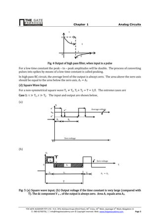
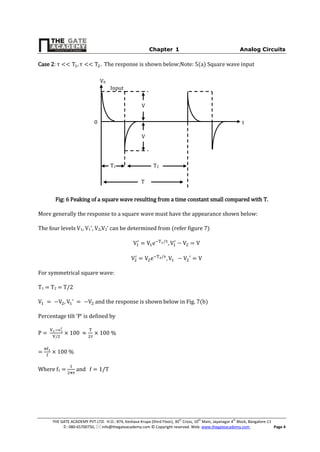
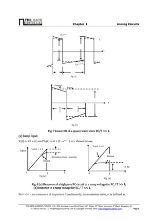
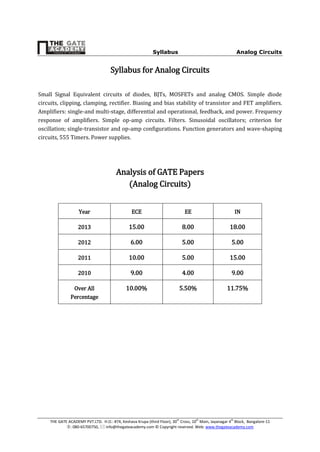
The document outlines a syllabus for analog circuits, including specific topics such as diode circuits, transistor biasing, frequency response, and operational amplifiers. It includes a structured approach to learning with chapters dedicated to theory, assignments, and solutions. Additionally, the document provides historical analysis of past GATE examination papers in electronics and electrical engineering related to analog circuits.

![Chapter-1 Analog Circuits
THE GATE ACADEMY PVT.LTD. H.O.: #74, Keshava Krupa (third Floor), 30th
Cross, 10th
Main, Jayanagar 4th
Block, Bangalore-11
: 080-65700750, info@thegateacademy.com © Copyright reserved. Web: www.thegateacademy.com Page 2
Fig. 2 Gain-frequency plot of high pass circuit
(b) Step Input:
Fig. 3 Output voltage of high pass circuit when input is a step voltage
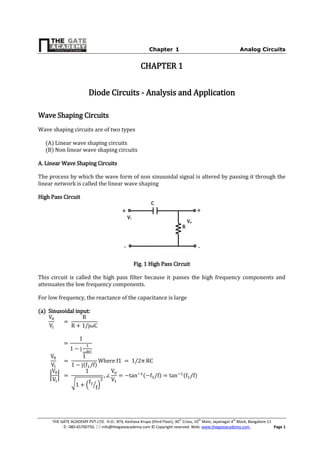
(t) = ( ) ( ) ( ) ( )
( ) = 1/C ( )
iR,
So ( ) 1/RC (t) dt + ( ) ( )
It is a single time constant circuit and a first order equation is obtained. The general solution of
any single time constant circuit can be written as,
( ) ( ) , here Vf = 0, Vi = V, Vo(t) = Ve- τwhere τ
(c) Pulse Input: ( ) [ ( ) ( )]
1)
2) ( )
τ
τ
( )
0
V
| |
1
0.707](https://image.slidesharecdn.com/analogcircuits-140517065448-phpapp02/85/Electronics-and-Communication-Engineering-Analog-circuits-THE-GATE-ACADEMY-8-320.jpg)