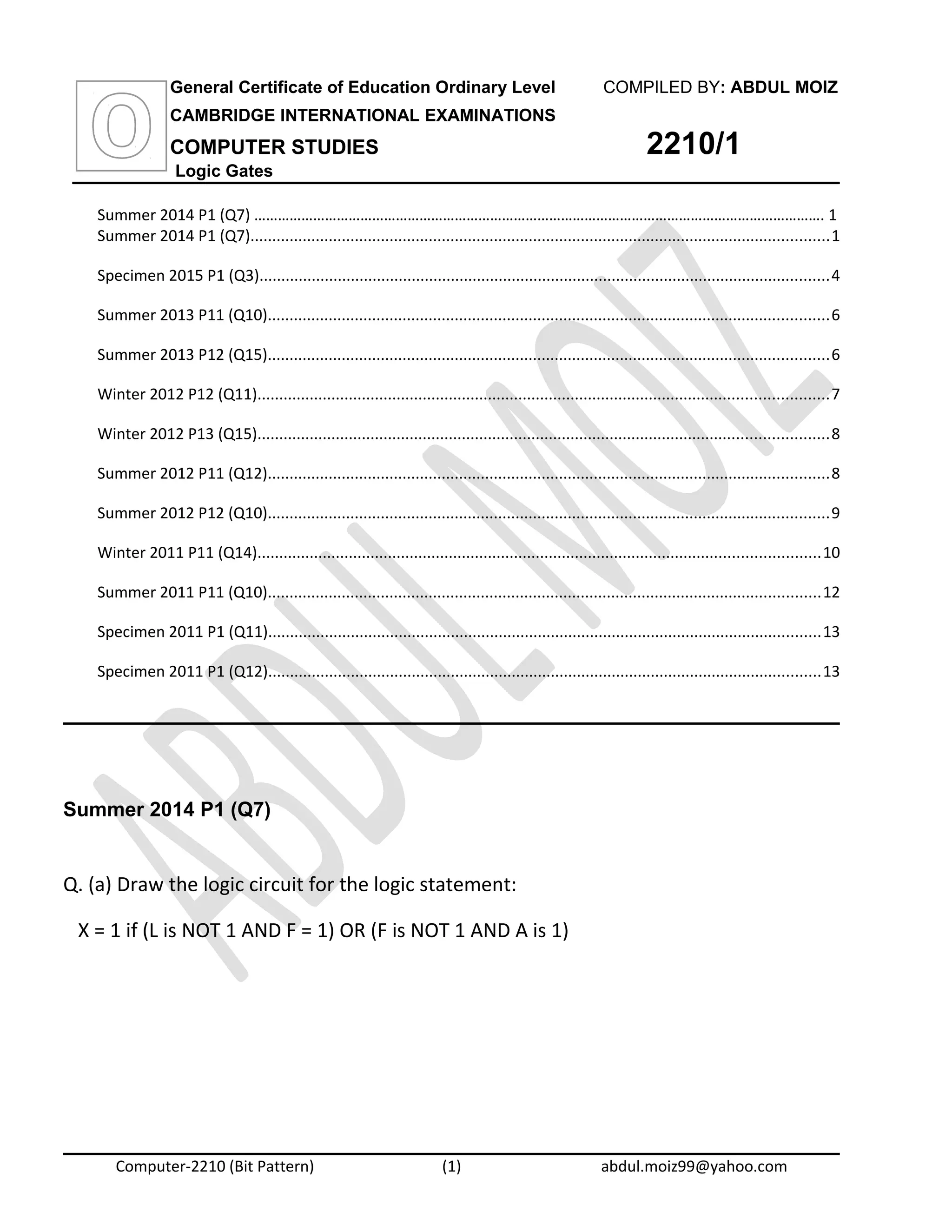
The document is a compilation of examination questions and specifications for the Cambridge International Examinations General Certificate of Education Ordinary Level in Computer Studies. It includes various logic circuit problems, truth tables, and alarms related to different scenarios such as chemical processes and nuclear reactors. Each question requires students to draw logic circuits and complete truth tables based on specified conditions.

![[5]
(b) Complete the truth table for the above system.
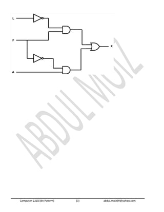
L F A
Working space
X
0 0 0
0 0 1
0 1 0
0 1 1
1 0 0
1 0 1
1 1 0
1 1 1
S O L U T I O N:
(a) 1 mark per correct logic gate (accept other gate symbols)
Computer-2210 (Bit Pattern) (2) abdul.moiz99@yahoo.com
L
F X
A](https://image.slidesharecdn.com/logicgatespapers-2-150829172039-lva1-app6892/85/Logic-Gates-O-level-Past-Papers-questions-2-320.jpg)
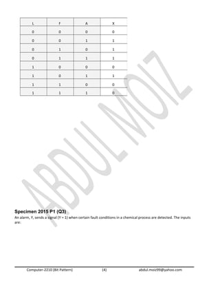
![The alarm, Y, returns a value of 1 if:
either temperature >= 120o
C AND stirrer bar is OFF
or acidity > 5 AND temperature < 120o
C
(a) Draw the logic circuit for the above system using these logic gates. [5]
Computer-2210 (Bit Pattern) (5) abdul.moiz99@yahoo.com](https://image.slidesharecdn.com/logicgatespapers-2-150829172039-lva1-app6892/85/Logic-Gates-O-level-Past-Papers-questions-5-320.jpg)
![(b) Complete the truth table for this alarm system. [4]
A T S Y
1 1 1
1 1 0
1 0 1
1 0 0
0 1 1
0 1 0
0 0 1
0 0 0
Summer 2013 P11 (Q10)
(a) (i) Complete the truth table for the logic circuit which is made up of NAND gates only. [2]
(ii) What single logic gate has the same function as the above logic circuit? [1]
(b) (i) Complete the truth table for the logic circuit.
(ii) What could replace the whole logic circuit? [1]
Summer 2013 P12 (Q15)
(a) Draw the logic circuit represented by the logic statement:
X = 1 if (B is NOT 1 AND S is NOT 1) OR (P is NOT 1 AND S is 1) [6]
Computer-2210 (Bit Pattern) (6) abdul.moiz99@yahoo.com](https://image.slidesharecdn.com/logicgatespapers-2-150829172039-lva1-app6892/85/Logic-Gates-O-level-Past-Papers-questions-6-320.jpg)
![b) Complete the truth table for the above logic statement. [4]
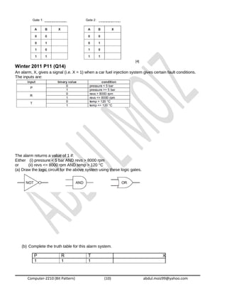
Winter 2012 P12 (Q11)
An alarm sounds when certain conditions occur in a nuclear reactor.
The output, X, of a logic circuit that drives the alarm must have a value of 1 if:
either carbon dioxide pressure too low and temperature < = 300°C
or water pressure > 10 bar and temperature > 300°C
The inputs to the system are:
(a) Draw the required logic circuit using AND, OR and NOT gates only. [5]
(b) Complete the truth table for the above system. [4]
P T W X
1 1 1
1 1 0
1 0 1
1 0 0
0 1 1
0 1 0
0 0 1
0 0 0
Computer-2210 (Bit Pattern) (7) abdul.moiz99@yahoo.com](https://image.slidesharecdn.com/logicgatespapers-2-150829172039-lva1-app6892/85/Logic-Gates-O-level-Past-Papers-questions-7-320.jpg)
![Winter 2012 P13 (Q15)
15 (a) Complete the truth table for the following logic circuit: [4]
A B C X
1 1 1
1 1 0
1 0 1
1 0 0
0 1 1
0 1 0
0 0 1
0 0 0
(b) The above logic circuit uses AND, OR and NOT gates.
Name another logic gate and complete its truth table. [3]
Name : _______________________________________________
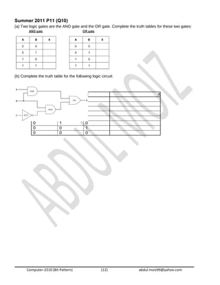
Summer 2012 P11 (Q12)
(a) (i) Complete the truth table for the following logic circuit, which is made up of NAND gates:
Computer-2210 (Bit Pattern) (8) abdul.moiz99@yahoo.com](https://image.slidesharecdn.com/logicgatespapers-2-150829172039-lva1-app6892/85/Logic-Gates-O-level-Past-Papers-questions-8-320.jpg)
![(ii) What single logic gate has the same function as the above logic circuit? [1]
b) Complete the truth table for the following logic circuit:
A B C X
1 1 1
1 1 0
1 0 1
1 0 0
0 1 1
0 1 0
0 0 1
0 0 0
Summer 2012 P12 (Q10)
(a) Complete the truth table for the following logic circuit, which is made up of NAND gates:
A B C X
1 1 1
1 1 0
1 0 1
1 0 0
0 1 1
0 1 0
0 0 1
0 0 0
(b) Name two other types of logic gates and complete their associated truth tables:
Computer-2210 (Bit Pattern) (9) abdul.moiz99@yahoo.com](https://image.slidesharecdn.com/logicgatespapers-2-150829172039-lva1-app6892/85/Logic-Gates-O-level-Past-Papers-questions-9-320.jpg)

![Specimen 2011 P1 (Q11)
Draw the truth table for the following logic network: [4]
A B C X
1 1 1
1 1 0
1 0 1
1 0 0
0 1 1
0 1 0
0 0 1
0 0 0
Specimen 2011 P1 (Q12)
Draw a logic network and truth table for the following logic problem:
“A sprinkler (S) is ON if
either temperature alarm (T) is ON and cooler alarm (C) is ON
or vent alarm (V) is OFF and cooler alarm (C) is ON” [9]
Working: ____________________________________________________________________
____________________________________________________________________________ [2]
Logic Network:
Truth Table:
T C V S
1 1 1
1 1 0
1 0 1
1 0 0
0 1 1
0 1 0
0 0 1
0 0 0
Computer-2210 (Bit Pattern) (13) abdul.moiz99@yahoo.com](https://image.slidesharecdn.com/logicgatespapers-2-150829172039-lva1-app6892/85/Logic-Gates-O-level-Past-Papers-questions-13-320.jpg)