Download to read offline
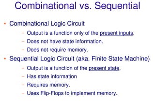

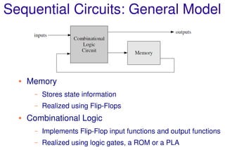
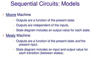
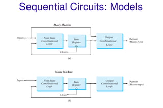
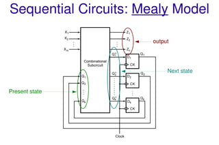
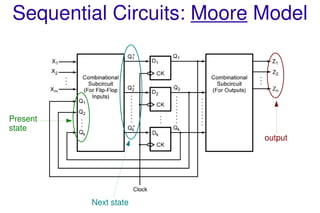
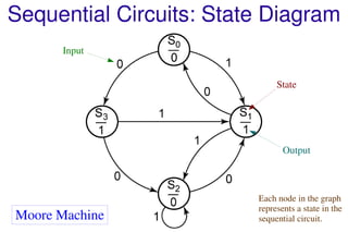
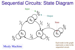
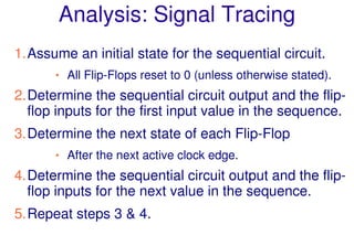

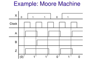

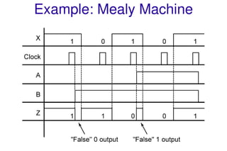

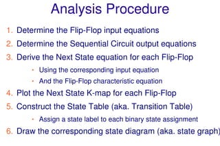


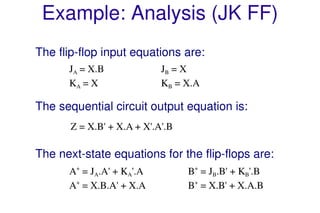


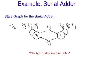


This document discusses sequential logic circuits and their analysis. It defines combinational and sequential logic, and synchronous and asynchronous circuits. There are two main types of sequential logic models - Moore and Mealy machines. Analysis of sequential circuits involves deriving their state tables and state diagrams from the circuit description. Examples show how to analyze circuits using D flip-flops, JK flip-flops, and a serial adder circuit. Multiple input state machines have state tables where the next state depends on all present inputs.