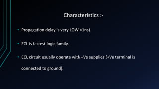
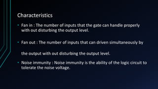
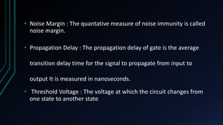
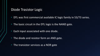
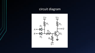
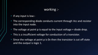
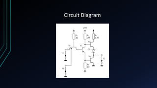
This document discusses different logic families including their characteristics, circuits, and workings. It covers Resistor Transistor Logic (RTL), Diode Transistor Logic (DTL), Transistor-Transistor Logic (TTL), and Emitter Coupled Logic (ECL). RTL uses resistors and transistors, DTL uses diodes and transistors, TTL provides faster operation using multiple transistors, and ECL is a non-saturated logic family that provides OR and NOR functions using differential amplifiers and emitter followers. The document compares their characteristics such as fan-in, fan-out, propagation delay, power dissipation, and noise immunity.


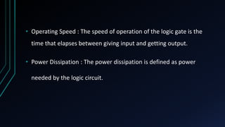


![• But at the same time we have L=+VCC, this voltage is applied on the
base of Q4
• As a result transistor Q3 is turned ON.
• Therefore, the output voltage is given by V0=+VCC-[Voltage drop in
R4+drop in diode ‘D’]
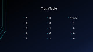
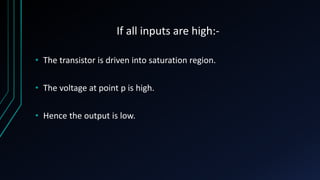
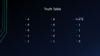
• A=1,B=1;
• When both input are high then emitter base junction of transistor
Q1 becomes reverse bias. Hence Q1 is turned off.
• However its collector base junction is forward bias, supplying base
current to the transistor Q2. Hence Q2 turns ON.](https://image.slidesharecdn.com/logicfamilies-200619165100/85/Logic-families-23-320.jpg)