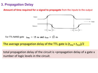
Logic families- Propagation Delay, Fan - In and Fan - Out -
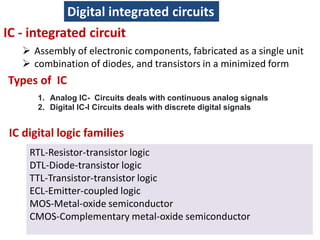
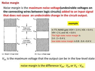
Noise Margin - RTL ,TTL,ECL, CMOS - Comparison of Logic
families - Implementation of combinational
logic/sequential logic design using standard ICs, PROM,
PLA and PAL, basic memory, static
ROM,PROM,EPROM,EEPROM EAPROM.