Downloaded 199 times

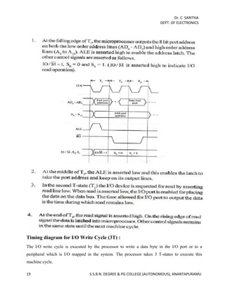


This document provides an overview of microprocessors and the 8085 microprocessor. It discusses the evolution of microprocessors from early business calculators and home computers to modern devices. It then describes the internal architecture of the 8085 microprocessor, including its functional blocks like the ALU, registers, flags, and buses. Finally, it outlines the five generations of microprocessors and provides details on the pin configuration and functions of the 8085 microprocessor.