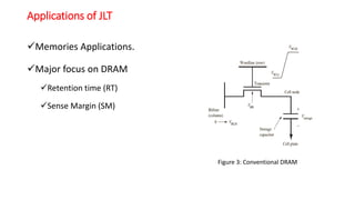
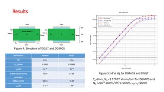
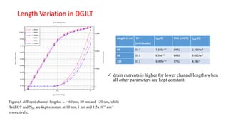
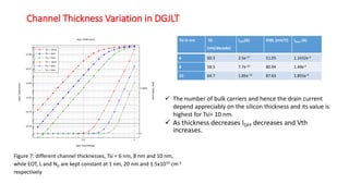
1. Presentation of Summer Research Project
On
“Performance Estimation of Junctionless Transistor and
its applications ”
Presented by
Durga Rao Gundu
(217EE1155)
DEPARTMENT OF ELECTRICAL ENGINEERING
NATIONAL INSTITUTE OF TECHNOLOGY ,ROURKELA
2. WHY Junctionless Transistor ??
Moore’s Law
“NO of transistors doubles every 18 months on a chip ”
Low Power
“Depends on VDD ”
Short Channel Effects
“Leakage Currents ”
Fabrication Challenges
“P-N junctions ”
Figure 1: Current trend in semiconductor industry
3. Structure and Operation of Junctionless Transistor
NO PN junction in source-channel-drain path.
Channel Region is highly doped (8*1018 -8*1019).
ΦMS = ΦM − (𝜒 +
𝐸 𝑔
2
+ 𝑘𝑇𝑙𝑛(
𝑁 𝐷
𝑛 𝑖
))
(a) subthreshold fully-depleted,
(b) linear partially-depleted,
(c) saturation partially-depleted,
(d) linear accumulated,
(e) linear accumulated & partially-depleted,
(f) saturation accumulated & partially depleted,
Figure 2: Current conditions depending on gate and drain
biases
4. COMPARISON OF JT AND JLT
JUNCTION TRANSISTOR JUNCTION LESS TRANSISTOR
1.High electric field 1.Less electric field (no decrease in
mobility)
2. Major carrier make itself barrier to
carrier scattering
2. No barrier, so high current drive
3.Complex and expensive Fabrication. 3. No annealing, implantation, easy
fabrication
4. Short channel effects 4. Reduced short channel effects
5. Surface conduction 5. Bulk conduction
6. Doping is low 6. Doping is high in the channel
5. Applications of JLT
Memories Applications.
Major focus on DRAM
Retention time (RT)
Sense Margin (SM)
Figure 3: Conventional DRAM
6. Results
Parameters DGMOS DGJLT
Wf 4.8ev 5.1ev
VTH (Volts) 0.5935 0.70633
IOFF(A) 2e-14 8e-16
Subthreshold swing
(mV/dec)
71.92 67.56
DIBL (mV/V) 58.63 76.57
ION (A) 2.1e-4 1.4e-4
Tsi=8nm, ND =1.5*1019 atoms/cm3 for DGMOS and
NA =21015 atoms/cm3 L=20nm, LD, LS =20nm
Figure 4: Structure of DGJLT and DGMOS
Figure 5: Id Vs Vg for DGMOS and DGJLT
7. Length Variation in DGJLT
Length in nm SS
(mV/decade)
IOFF(A) DIBL (mV/V) IDsat (A)
60 57.7 7.325e-13 69.52 1.1632e-4
80 55.5 6.56e-13 64.65 9.6012e-5
120 57.1 6.009e-13 57.52 8.28e-5
Figure.6 different channel lengths, L = 60 nm, 80 nm and 120 nm, while
Tsi,EOT and ND, are kept constant at 10 nm, 1 nm and 1.5x1019 cm-3
respectively,
drain currents is higher for lower channel lengths when
all other parameters are kept constant.
8. Channel Thickness Variation in DGJLT
Tsi in nm SS
(mV/decade)
IOFF(A) DIBL (mV/V) IDsat (A)
6 60.3 2.5e-17 51.05 1.1632e-4
8 58.5 7.7e-16 80.94 1.49e-4
10 64.7 1.85e-13 87.63 1.855e-4
Figure 7: different channel thicknesses, Tsi = 6 nm, 8 nm and 10 nm,
while EOT, L and ND are kept constant at 1 nm, 20 nm and 1.5x1019 cm-3
respectively
The number of bulk carriers and hence the drain current
depend appreciably on the silicon thickness and its value is
highest for Tsi= 10 nm.
As thickness decreases IOFF decreases and Vth
increases.
9. Concentration Variation in DGJLT
Concentration
in 1019 cm-3
SS
(mV/decade)
IOFF(A) DIBL (mV/V) IDsat (A)
1 64.9 2.2e-15 74.31 1.432e-4
1.3 66.6 3.1e-14 83.78 1.69e-4
1.5 68.7 1.85e-13 88.52 1.855e-4
Figure 8: different channel doping concentrations. ND= 1x1019 cm-3.
1.3x1019cm-3 and 1.5x1019cm-3, while at Tsi, L and EOT are kept constant
at 10 nm. 20 nm and 1 nm respectively.
Drain current is highest for ND = 1.5x1019 cm-3.
As concentration increases IOFF increases
As concentration increases Vth decreases.
10. Conclusion
This Structure is having near Ideal subthreshold slope, close to 60mv/dec at
room temperature.
This is best for very thin silicon thickness as Nanowires.
Controlling the cross section appears to be a critical key parameter for threshold
voltage tuning.
As SS is near to ideal and Ioff is less which make JLT better for Digital Application.
11. Future Work
Optimization of the device to get better performance.
Use the optimized device in designing the DRAM to improve the two important
parameters Retention time (RT) and Sense Margin (SM).
12. References
J.-P. Colinge et al., “Nanowire transistors without junctions,” Nature Nano technol., vol. 5, pp. 225–229, Feb.
2010, doi:10.1038/nnano.2010.15.
International Technology Roadmap for Semiconductors, 2015, www.itrs.net.
S.-J. Choi, D.-I. Moon, S. Kim, J. Duarte and Y.-K. Choi, "Sensitivity of threshold voltage to nanowire width
variation in junctionless transistors". IEEE Electron Device Lett..vol. 32, no. 2, pp. 125-127. Feb. 2011.
Y. J. Yoon, J. H. Seo, M. S. Cho, B. G. Kim, S. H. Lee, and I. M. Kang, “Capacitorless one-transistor dynamic
random access memory based on double-gate GaAs junctionless transistor,” Jpn. J. Appl. Phys., vol. 56, pp.
1–6, Apr. 2017, doi: 10.7567/JJAP.56.06GF01.