Downloaded 184 times
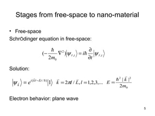
()( 00 RlrVrV
+=
r
e
rV
ε
2
0 )( −=
kne Etrki
kn
)/( −
=ψ
effm
k
E
2
|| 22
=](https://image.slidesharecdn.com/introductiontonano-materials-140622235937-phpapp02/85/Introduction-to-nano-materials-6-320.jpg)
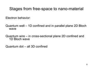
![7
Stages from free-space to nano-material
• Nano-material
SchrÖdinger equation in nano-material:
with artificially generated extra potential contribution:
Solution:
trtrnano
t
irVrV
m
,,0
2
0
)]()(
2
[
ψψ
∂
∂
=++∇−
)(rVnano
knrFe kn
iEt
kn
)(,
/−
=ψ](https://image.slidesharecdn.com/introductiontonano-materials-140622235937-phpapp02/85/Introduction-to-nano-materials-7-320.jpg)
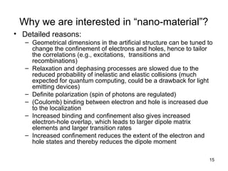

This document provides an introduction to nano-materials. It defines nano-materials as artificial semiconductor structures with dimensions on the nanometer scale, including quantum wells, wires, and dots. Electron behavior changes from plane waves in free space, to Bloch waves in bulk semiconductors, to discrete energy levels in low-dimensional nano-structures. Nano-materials are of interest because they allow tailoring of electronic and optical properties by controlling geometric confinement. Common fabrication methods include lithography and self-organized growth to achieve sizes less than 100nm for full quantum confinement effects. Nano-materials demonstrate properties like ballistic transport, tunneling, and quantized energy levels that enable applications in light sources, detectors, and electronic devices