SlideShare a Scribd company logo
1 of 7
Download to read offline
International Research Journal of Engineering and Technology (IRJET) e-ISSN: 2395 -0056
Volume: 04 Issue: 03 | Mar -2017 www.irjet.net p-ISSN: 2395-0072
© 2017, IRJET | Impact Factor value: 5.18 | ISO 9001:2008 Certified Journal | Page 1932
Quantitative Modeling and Simulation of Single-Electron Transistor
Shobhit Srivastava1, Ranjeet Pathak2
1M.Tech, Student, Department of E&C Engineering, U.I.T. Allahabad, U.P (AKTU, University), India
2Assistant Prof., Department of E&C Engineering, United Institute of Technology, Allahabad, Uttar Pradesh, India
------------------------------------------------------------------***-----------------------------------------------------------------
Abstract— The Single electron transistor (SET) is a new
nano scaled switching device that retains their scalability
even on an atomic scale, which can offer ultra-low power
consumption and high operating speed.
SET has some attractive feature like unique coulomb
blockade oscillation characteristic, and nano-scale size. It
is seen that energy quantization mainly increases the
Coulomb blockade area and Coulomb blockade oscillation
periodicity, and thus, affects the SET circuit performance.
The transfer of charge onto the island becomes quantized
as the voltage increase, leading to the current, so-called
coulomb staircase. For it two conditions are required
mainly, in first condition the electron thermal fluctuations
energy smaller than the coulomb energy and in second
condition, the tunnel effect itself should be weak enough to
prevent the charge of the tunneling electrons from
becoming delocalized over the two electrodes of the
junctions.
The goal of this paper is to discuss about the DC
characteristics of SET and the effect on characteristics of
SET by variation of various physical parameters, is
analyzed by MATLAB Simulink.
Key Words—Quantum tunneling, Coulomb blockade (CB),
quantum dot (QD), energy quantization, single electron
transistor (SET).
1. INTRODUCTION
Our world is without doubt built on the power of the
transistor, a microscopic electronic switch used to perform
digital logic. Right now, we are able to fit enough of these
tiny devices onto a microchip to allow us to perform
several billion operations in a single second, and are seeing
a double in the speed of these microchips every 18 months.
In order to keep up with this incredible rate of speed
increase, transistors are becoming smaller and smaller, to
the point where in the very near future, they will begin to
not only feel the effects of quantum mechanics on their
operation, but will have to take quantum mechanics into
account as the dominant force in their engineering.
Most transistors today are MOSFETs, where a
semiconductor source and drain of one doping type are
separated by an oppositely doped bulk semiconductor. The
bulk semiconductor is then separated by a layer of oxide
from a gate electrode between the source and the drain. As
the gate bias is changed, the bias causes the formation of a
conducting channel in the bulk material between the
source and drain, allowing current to flow and thus
turning the switch on. In a single electron transistor,
however, charge moves by utilizing the effect of quantum
tunneling. Instead of creating a channel of charge carriers
between the source and drain electrodes, a single electron
transistor utilizes two junctions where tunneling is the
dominant method of electron transport to control the
movement of single electrons through the device.
2. BASIC THEORY
2.1 QUANTUM TUNNELING
A single electron transistor is based on the idea of
quantum tunneling.
In classical physics, when an electron is in a potential, it is
unable to go anywhere, where the potential is higher than
the energy of the electron fig.1.
Fig. 1: Classical theory of electron Tunneling
However, According to the laws of quantum mechanics,
when the size of the barrier is very small, the wave
properties of the electron become relevant. And there is a
non vanishing (larger than zero) probability for an
electron on one side of the barrier to reach the other side.
Fig. 2: quantum tunneling of electron
2.2 COULOMB BLOCKADE
In physics, a Coulomb blockade (abbreviated CB), named
after Charles-Augustin de Coulomb's electrical force, is the
increased resistance at small bias voltages of an electronic
International Research Journal of Engineering and Technology (IRJET) e-ISSN: 2395 -0056
Volume: 04 Issue: 03 | Mar -2017 www.irjet.net p-ISSN: 2395-0072
© 2017, IRJET | Impact Factor value: 5.18 | ISO 9001:2008 Certified Journal | Page 1933
device comprising at least one low-capacitance tunnel
junction. Because of the CB, the resistances of devices are
not constant at low bias voltages, but increase to infinity
for zero bias (i.e. no current flows).
Due to the discreteness of electrical charge, current
through a tunnel junction is a series of events in which
exactly one electron passes (tunnels) through the tunnel
barrier. The tunnel junction capacitor is charged with one
elementary charge by the tunneling electron, causing a
voltage buildup V= where e is the elementary charge of
1.6× coulomb and C the capacitance of the junction. If
the capacitance is very small, the voltage buildup can be
large enough to prevent another electron from tunneling.
The electrical current is then suppressed at low bias
voltages and the resistance of the device is no longer
constant. The increase of the differential resistance around
zero bias is called the Coulomb blockade.
2.3 CONDITION FOR COULOMB BLOCKED
To achieve the Coulomb blockade, three criteria have to be
met:
The bias voltage must be lower than the elementary charge
divided by the self capacitance of the island:
V < (1)
The thermal energy in the source contact and the thermal
energy in the island must be below the charging energy or
else the electron will be able to pass the QD via thermal
excitation
k T
e
c
(2)
The tunnelling resistance Rt, should be greater than h/e2
which is derived from Heisenberg’s uncertainty principle.
h
e
(3)
Rt 5813Ω
The Coulomb energy is given by
(4)
Where e is the charge on an electron and is the total
capacitance of the source and drain junctions and the gate
capacitor.
2.4 SINGLE ELECTRON TRANSISTOR
The simplest device, in which the effect of coulomb
blockade can be observed, is the so-called single electron
transistor.
It consists of two electrodes known as the drain and the
source, connected through tunnel junctions to one
common electrode with a low self- capacitance known as
the island. The electrical potential of the island can be
tuned by a third electrode, known as the gate, capacitive
coupled to the island, As shown in fig.3
Fig. 3: Single electron transistor
Fig. 4: capacitance model for the SET
3. MODELING AND SIMULATION METHODOLOGY
The Modeling and simulation of Single Electron Transistor
is done using MATLAB Simulink. The SET circuit consisting
of a dot between the source and drain electrodes
separated by tunnel capacitors and . Both tunnel
capacitors and have tunnel resistances and ,
respectively. The dot is also coupled to the gate electrode
with capacitor in order to control the current flow. The
total capacitance between the dot and the outer
environment can be written as , where
(5)
Fig. 5: Equivalent circuit of SET
There are four main equations for current-voltage
characteristics of single electron circuits, i.e., free energy
change ΔF, tunneling probability/rate ɼ, steady state
master equation and current equation I as follows.
International Research Journal of Engineering and Technology (IRJET) e-ISSN: 2395 -0056
Volume: 04 Issue: 03 | Mar -2017 www.irjet.net p-ISSN: 2395-0072
© 2017, IRJET | Impact Factor value: 5.18 | ISO 9001:2008 Certified Journal | Page 1934
3.1 Free energy change:
ΔF1 (n1 n )
e
*
e
( e-Qo) ( g ) g g+ (6)
ΔF (n1 n )
e e
e-Qo 1 g g (7)
Equations (6) and (7) are used to calculate the free
(electrostatic) energy change ΔF of the system due to the
one electron tunneling event. It is important to be noted
that only tunneling events decreasing the electrostatic
energy (and dissipating the difference) are possible.
3.2 Tunneling probability/rate:
The most important requirement for occurrence of single
electron tunneling is that the total energy of the system
must Decrease due to one electron tunneling. Electron
tunneling rate in tunnel junction ( ) can be calculated from
derivation of Fermi Golden Rule.
1
R1e
[
ΔF1
1- exp(
ΔF1
kbT
)
] (8)
1
R e
[
ΔF
1- exp(
ΔF
kbT
)
] (9)
The values ΔF from equations (6) and (7) are used to
calculate electron tunneling probability in the equations
(8) and (9), respectively. The tunneling of a single electron
through a particular tunnel junction is always a random
event, with a certain rate (i.e., probability per unit time)
which depends solely on the ΔF.
3.3 Steady State Master equation:
p( ) -
( ) 1 ( ) p( 1) -
( 1) 1 ( 1) (10)
( ) e ∑ p- 1 ( ) – 1
-
( ) (11)
e ∑ p-
( ) – -
( ) (12)
Equation (10) expresses the Master equation in steady
state, resulting the value of p (N), which is necessary to be
used for the current calculation in equation (11) and (12).
where e is the elemental charge, kb is the Boltzmann
constant, T is the temperature, N is the number of
electrons in the dot, n1 and n2 are a number of electrons
flows through the capacitor C1 and capacitor C2,
respectively, Qo is the background charge and +/- express
that the electron tunnels through the capacitor with the
direction from left to the right and from right to the left,
respectively.
The iterative algorithm of master equation method is
presented in Figure
Fig. 6: algorithm of master equation
4. FABRICATION PARAMETERS:
The main fabrication parameters are source and drain
tunnel junction capacitances, side gate capacitance, and
control gate capacitance, are given below
(13)
Where Cg, Lg, Wch and Tgox are side gate capacitance, side
gate length, channel width, and side gate oxide thickness
respectively.
(14)
Where Cc, Lc, & Tcox are control gate capacitance, control
gate length and control gate oxide thickness respectively.
Before any electron tunneling, the tunneling junctions act
as capacitances so it could be written as:
(15)
Where C1, C2, and Tsi are source capacitance, drain
capacitance, and channel thickness, respectively .But here
in this paper I only assume that SET is three terminal
International Research Journal of Engineering and Technology (IRJET) e-ISSN: 2395 -0056
Volume: 04 Issue: 03 | Mar -2017 www.irjet.net p-ISSN: 2395-0072
© 2017, IRJET | Impact Factor value: 5.18 | ISO 9001:2008 Certified Journal | Page 1935
devices and neglect to Cc capacitance effect.
Some external parameters (V ,Vg, T and qo) and some
device parameters (C1, C2, Cg, R1 and R2), effects the
properties of the SET but there is difference between them
parameter like device parameter may be set before
fabrication and external parameter may be adjust
according to environmental condition given in below table
1 [9]
Description
Value
Wch 15nm
Lg 20nm
Lc 10nm
Tgox 10nm
Tcox 5nm
Tsi 15nm
Table 1
Represents the approximate values of the parameters that
is used for the fabrication of the silicon-based dual-gate
SET [9].
5. RESULT AND DISCUSSION
The modeling of single electron transistor is based on its
stability criteria for selecting parameters in such a way
that all the characteristic of SET comes within the stability
region, so below there is a brief discussion on stability and
curve based on master’s equation of SET.
5.1 Stability plot for SET:
The energy which determines electron transportation
through a single-electron device is Helmholtz free energy
which is defined as difference between total energy stored
in the device and the work done by power source. Total
energy stored includes all of energy components when an
island is charged with an electron. For a SET with source
and control gate terminals grounded, and drain and side
gate terminals based at Vds and Vgs, the free energy has
been formulated as following.
(16)
Here E is the electrostatic energy, Qg is the charge of the
side gate capacitance, and Qd is the charge at drain tunnel
junction capacitance. The change of Helmholtz free energy
is calculated as:
(17)
Where Fi and Ff are the Helmholtz free energy of the
system before and after an electron tunneling happens
respectively.
A tunneling could only happen if is negative. For a logic
operation, i.e., where the number of electrons in the island
is 0 or 1, is defined as:
F ds ( 1⁄ ) gs ( g
⁄ ) (18)
For the electron tunneling of the island to the source
terminal is:
F - ds
( 1⁄ ) - gs ( g
⁄ ) (19)
If an electron tunnels from the island to the drain terminal,
is defined as:
( ⁄ ) ( ⁄ ) (20)
For the electron tunneling of the drain terminal to the
island, F is:
( ⁄ ) ( ⁄ ) (21)
The above equation (18-21) obtained from the equation 6
& 7.
Now in SET, characteristic is known as
stability plot. This plot is obtained by setting equations
(18-21 equals to zero. Thus four lines’ equation will be
obtained so that their cross creates a rhombus as shown
below.
Slop of these lines has been formulated as following:
If electron tunnels from the island to the drain terminal
and vice versa lines’ slope is:
S1
( g )
⁄ (22)
If electron tunnels from the source terminal to the island
and vice versa lines’ slope is:
g
⁄ (23)
The stability plot of SET is illustrate in fig. (7)
International Research Journal of Engineering and Technology (IRJET) e-ISSN: 2395 -0056
Volume: 04 Issue: 03 | Mar -2017 www.irjet.net p-ISSN: 2395-0072
© 2017, IRJET | Impact Factor value: 5.18 | ISO 9001:2008 Certified Journal | Page 1936
Fig.7. stability plot of SET for n=0
In this Figure the rhombus outside regions corresponds to
regions with an integer number of the excess electrons on
the island.
In rhombus inside, there is no excess electron on the island
(The Coulomb Blocked Region).
But if charge will be present in this island region then
stability criteria may be effected significantly, the stability
region will be shifted in the right or left direction depend
on the charge on the island, n = ..-2, -1 1 … as shown in
figure 8. Here n=1, 2 represents number of electron in
quantum dot, n=0 shows empty quantum dot and n=-1,-2
shows holes in quantum dot.
Fig. 8 shift in stability region
5.2 Current oscillation on variation in Vgs
For logic operation, if Vgs is increased and Vds is kept
constant below the Coulomb blocked,| | , the current
will oscillate with the period of Figure (9). This is
because of Vds is not applied or increasing in accordance
to pull the electron from source to QD to Drain for a
continuous current. And thus Vgs is showing the control
over transportation of electron from source to drain.
Fig. 9. current oscillation with logical operation on Vgs
Now to analysis the dc characteristic of SET, firstly it is
assume that Vds may be zero or may have any fixed value.
From equation 13-15, It is shown in Fig.10 that, by
increase of the channel width, the Coulomb blockade
region becomes narrower and the oscillation period of the
drain current decreases. This is because by increase of the
channel width, all capacitances change but the slope of S2
remains constant and the slope of S1 reduces, so rhombus
inside area or the Coulomb blocked region decreases. In
addition, the side gate capacitance decrease, therefore the
oscillation period of the drain current decreases.
Fig 10: Variation effect in the channel width on the Ids-Vgs
Fig.11 shows the side gate length variation effect on the
Ids-Vgs. It is demonstrated that, the increase of the side
gate length causes the Coulomb blocked region to become
narrower and the oscillation period of the drain current to
become less. According to the equations (13-15), by
increase of the side gate length, all capacitances are
changed but the slope of S2 remains constant and the slope
of S1 reduces, so the Coulomb blocked region decreases.
The variation effect in the side gate length is less that the
Variation effect in the channel width.
International Research Journal of Engineering and Technology (IRJET) e-ISSN: 2395 -0056
Volume: 04 Issue: 03 | Mar -2017 www.irjet.net p-ISSN: 2395-0072
© 2017, IRJET | Impact Factor value: 5.18 | ISO 9001:2008 Certified Journal | Page 1937
Fig 11: Variation effect in the gate length on the Ids-Vgs
It is demonstrated that, by increase of the side gate oxide
thickness, the Coulomb blocked region becomes wider and
the oscillation period of the drain current increases.
According to equation 13-15, increase of this parameter
causes the side gate capacitance to become less and the
slope of both S1 and S2 to increase. Shown in fig12
Fig12: Variation effect in the gate oxide thickness on the
Ids-Vgs
Fig 13: Variation effect in temperature on the Ids-Vgs
Above fig 13 demonstrates the temperature variation
effect on the Ids-Vgs characteristic
5.3 Stair-Case Ids current
For simulations purpose it is assumed that Vds is varied
from -1v to 1v, T=20 K and assume gate voltage Vg=0 in
case of Ids-Vds characteristic and assume Vg varied from -0.2v
to 0.2v,Vds=18mv and T=2k . and from equation (11) and
(12) we can plot Ids –Vds characteristic plot shows the
device is symmetric.
Fig.14. I–V characteristic plot.
As shown as the coulomb staircase effect in Ids-Vds
characteristic the may be too much effected by
temperature variation as shown in Fig.15
Fig15: temperature variation effect on the Ids-Vds
There is an increase in the value of current as temperature
increases and there is also a very small difference in the
value of the current when temperature becomes at high
value range but there is all must reverse result will be
obtained when increase in the value of background
charges as shown in Fig.16
International Research Journal of Engineering and Technology (IRJET) e-ISSN: 2395 -0056
Volume: 04 Issue: 03 | Mar -2017 www.irjet.net p-ISSN: 2395-0072
© 2017, IRJET | Impact Factor value: 5.18 | ISO 9001:2008 Certified Journal | Page 1938
Fig 16: Background charge variation effect on the Ids-Vds
So this is good for SET Ids - Vds characteristic that there are
no charges in the island.
6. CONCLUSION
In conclusion, I have demonstrated the electrical
characteristic of SET by using Master Equation approach
and show a fairly accurate result with experimental data.
Evidently, staircase pattern of I-V characteristic are clearly
obtained as the main role of coulomb blockade effect in the
SET system.
This research paper focuses the theoretical discussion of
basic principle of SET with importance of SET in the era of
nanotechnology to provide low power consumption and
high operating speed in the field of VLSI design for the
fabrication of various electronic devices. SET has proved
its value as tool in scientific research. The main problem in
nanometer era is the fabrication of nano scale devices that
can be achievable by the use of SET.
7. REFRENCES
[1] Frans Willy and Yudi Darma, “Modeling and simulation
of single electron transistor with master equation
approach” 6th Asian Physics Symposium OP Publishing
Journal of Physics: Conference Series 739 (2016) 012048
[2] Sheng Wang “Analytical Expressions and umerical
simulation of single electron spectroscopy” Department of
Physics, University of Science and Technology of China,
Hefei, 230026, Sep 2013
[3] Surya Shankar Dan and Santanu Mahapatra, “Analysis
of Energy Quantization Effects on Single-Electron
Transistor Circuits” IEEE Transactions on nanotechnology,
vol. 9, no. 1, January 2010
[4] Ahmed Shariful Alam, Abu Rena Md. Mustafa Kamal,
Md. Nasmus Sakib Khan Shabbir, Atiqul Islam, “Single
Electron Transistors (SET) substituting MOSFETs to
Reduce Power Consumption of an nverter ircuit” nd
Int'l Conf. on Electrical Engineering and Information &
Communication Technology (ICEEICT) 2015
[5] Vinay Pratap Singh, Arun Agrawal, Shyam Babu Singh,
“Analytical Discussion of Single Electron Transistor (SET),
International Journal of Soft Computing and Engineering
(IJSCE) ISSN: 2231-2307, Volume-2, Issue-3, July 2012
[6] K.Miyaji, M. Saitoh and T. Hiramoto “ ompact
analytical model for room- temperature operating silicon
single-electron transistors with discrete quantum levels”,
IEEE Trans. Nanotechnology, vol. 5, May 2006.
[7] A. Boubaker, M. Troudi , “A spice model for single
electron transistor applications at low temperatures:
inverter and ring oscillator” nternational Conference on
Design & Technology of Integrated Systems in Nano scale
Era, 2008
[8] Pankaj Kumar Sinha and Sanjay S “Single Electron
Transistor and its Simulation methods” nternational
Journal of Engineering Development and Research (IJEDR)
2014 | Volume 2, Issue 2 | ISSN: 2321-9939
[9] Khadijeh Feizi, Saeed Haji Nasiri, “DC Characteristic
Analysis of Single-Electron Transistor Based on MIB
Model”, International Conference on Nanotechnology and
Biosensors (2011) IACSIT Press, Singapore
8. BIOGRAPHIES
Shobhit Srivastava, born in
Varanasi, U.P., India, on June 22,
1990. He received the B.Tech.
degree in E&C Engineering from
UPTU University, UP, India in
2011 and Pursuing M.Tech from
the Department of E&C
Engineering, from Dr. A.P.J. Abdul
Kalam Technical University, UP,
India. His current research
interests include device reliability,
modelling, optimization and
design of integrated circuits for Nano Technology.

More Related Content

What's hot

Study of Logic Gates Using Quantum Cellular Automata
Study of Logic Gates Using Quantum Cellular AutomataStudy of Logic Gates Using Quantum Cellular Automata
Study of Logic Gates Using Quantum Cellular Automataidescitation
 
A short Commentary on Quantum-dot Cellular Automata (QCA)
A short Commentary on Quantum-dot Cellular Automata (QCA)A short Commentary on Quantum-dot Cellular Automata (QCA)
A short Commentary on Quantum-dot Cellular Automata (QCA)Soudip Sinha Roy
 
Multiscale-Contracted Variational Quantum Eigensolver
Multiscale-Contracted Variational Quantum EigensolverMultiscale-Contracted Variational Quantum Eigensolver
Multiscale-Contracted Variational Quantum Eigensolverhikaruwakaura
 
Adiabatic Logic Based Low Power Carry Select Adder for future Technologies
Adiabatic Logic Based Low Power Carry Select Adder for future TechnologiesAdiabatic Logic Based Low Power Carry Select Adder for future Technologies
Adiabatic Logic Based Low Power Carry Select Adder for future TechnologiesIJMER
 
Ch1 lecture slides Chenming Hu Device for IC
Ch1 lecture slides Chenming Hu Device for IC Ch1 lecture slides Chenming Hu Device for IC
Ch1 lecture slides Chenming Hu Device for IC Chenming Hu
 
Design and Implementation of Low Power 16-bit Carry-lookahead Adder using Adi...
Design and Implementation of Low Power 16-bit Carry-lookahead Adder using Adi...Design and Implementation of Low Power 16-bit Carry-lookahead Adder using Adi...
Design and Implementation of Low Power 16-bit Carry-lookahead Adder using Adi...IRJET Journal
 
Logic gates using quantum dots
Logic gates using quantum dotsLogic gates using quantum dots
Logic gates using quantum dotsRohit Kumar Mandal
 
4x4-bit 2PASCL Multiplier by Nazrul Anuar Nayan
4x4-bit 2PASCL Multiplier by Nazrul Anuar Nayan4x4-bit 2PASCL Multiplier by Nazrul Anuar Nayan
4x4-bit 2PASCL Multiplier by Nazrul Anuar Nayannazrulanuar
 

What's hot (20)

Short-Channel Effects in MOSFET
Short-Channel Effects in MOSFETShort-Channel Effects in MOSFET
Short-Channel Effects in MOSFET
 
High Electron Mobility Transistor
High Electron Mobility TransistorHigh Electron Mobility Transistor
High Electron Mobility Transistor
 
Carrier scattering and ballistic transport
Carrier scattering and ballistic transportCarrier scattering and ballistic transport
Carrier scattering and ballistic transport
 
CNTFET
CNTFETCNTFET
CNTFET
 
Electrical characteristics of MOSFET
Electrical characteristics of MOSFETElectrical characteristics of MOSFET
Electrical characteristics of MOSFET
 
Advanced MOSFET
Advanced MOSFETAdvanced MOSFET
Advanced MOSFET
 
Varactor diode
Varactor diodeVaractor diode
Varactor diode
 
Study of Logic Gates Using Quantum Cellular Automata
Study of Logic Gates Using Quantum Cellular AutomataStudy of Logic Gates Using Quantum Cellular Automata
Study of Logic Gates Using Quantum Cellular Automata
 
A short Commentary on Quantum-dot Cellular Automata (QCA)
A short Commentary on Quantum-dot Cellular Automata (QCA)A short Commentary on Quantum-dot Cellular Automata (QCA)
A short Commentary on Quantum-dot Cellular Automata (QCA)
 
Multiscale-Contracted Variational Quantum Eigensolver
Multiscale-Contracted Variational Quantum EigensolverMultiscale-Contracted Variational Quantum Eigensolver
Multiscale-Contracted Variational Quantum Eigensolver
 
Adiabatic Logic Based Low Power Carry Select Adder for future Technologies
Adiabatic Logic Based Low Power Carry Select Adder for future TechnologiesAdiabatic Logic Based Low Power Carry Select Adder for future Technologies
Adiabatic Logic Based Low Power Carry Select Adder for future Technologies
 
Ch1 lecture slides Chenming Hu Device for IC
Ch1 lecture slides Chenming Hu Device for IC Ch1 lecture slides Chenming Hu Device for IC
Ch1 lecture slides Chenming Hu Device for IC
 
Lecture 6: Junction Characterisation
Lecture 6:   Junction CharacterisationLecture 6:   Junction Characterisation
Lecture 6: Junction Characterisation
 
Design and Implementation of Low Power 16-bit Carry-lookahead Adder using Adi...
Design and Implementation of Low Power 16-bit Carry-lookahead Adder using Adi...Design and Implementation of Low Power 16-bit Carry-lookahead Adder using Adi...
Design and Implementation of Low Power 16-bit Carry-lookahead Adder using Adi...
 
2.4.6prefix
2.4.6prefix2.4.6prefix
2.4.6prefix
 
Lb2418671870
Lb2418671870Lb2418671870
Lb2418671870
 
Logic gates using quantum dots
Logic gates using quantum dotsLogic gates using quantum dots
Logic gates using quantum dots
 
4x4-bit 2PASCL Multiplier by Nazrul Anuar Nayan
4x4-bit 2PASCL Multiplier by Nazrul Anuar Nayan4x4-bit 2PASCL Multiplier by Nazrul Anuar Nayan
4x4-bit 2PASCL Multiplier by Nazrul Anuar Nayan
 
Unit 1
Unit 1Unit 1
Unit 1
 
Tunnel diode
Tunnel diodeTunnel diode
Tunnel diode
 

Similar to Quantitative Modeling and Simulation of Single-Electron Transistor

SINGLE ELECTRON TRANSISTOR: APPLICATIONS & PROBLEMS
SINGLE ELECTRON TRANSISTOR: APPLICATIONS & PROBLEMSSINGLE ELECTRON TRANSISTOR: APPLICATIONS & PROBLEMS
SINGLE ELECTRON TRANSISTOR: APPLICATIONS & PROBLEMSVLSICS Design
 
Single Electron Transistor: Applications & Problems
Single Electron Transistor: Applications & Problems  Single Electron Transistor: Applications & Problems
Single Electron Transistor: Applications & Problems VLSICS Design
 
Introduction gadgets have gained a lot of attention.pdf
Introduction gadgets have gained a lot of attention.pdfIntroduction gadgets have gained a lot of attention.pdf
Introduction gadgets have gained a lot of attention.pdfbkbk37
 
Effect of mesh grid structure in reducing hot carrier effect of nmos device s...
Effect of mesh grid structure in reducing hot carrier effect of nmos device s...Effect of mesh grid structure in reducing hot carrier effect of nmos device s...
Effect of mesh grid structure in reducing hot carrier effect of nmos device s...ijcsa
 
DESIGN OF DIFFERENT DIGITAL CIRCUITS USING SINGLE ELECTRON DEVICES
DESIGN OF DIFFERENT DIGITAL CIRCUITS USING SINGLE ELECTRON DEVICESDESIGN OF DIFFERENT DIGITAL CIRCUITS USING SINGLE ELECTRON DEVICES
DESIGN OF DIFFERENT DIGITAL CIRCUITS USING SINGLE ELECTRON DEVICESmsejjournal
 
DESIGN OF DIFFERENT DIGITAL CIRCUITS USING SINGLE ELECTRON DEVICES
DESIGN OF DIFFERENT DIGITAL CIRCUITS USING SINGLE ELECTRON DEVICESDESIGN OF DIFFERENT DIGITAL CIRCUITS USING SINGLE ELECTRON DEVICES
DESIGN OF DIFFERENT DIGITAL CIRCUITS USING SINGLE ELECTRON DEVICESmsejjournal
 
Single electron transistomy
Single electron transistomySingle electron transistomy
Single electron transistomyPranoti Bachhav
 
The Performance of an Integrated Transformer in a DC/DC Converter
The Performance of an Integrated Transformer in a DC/DC ConverterThe Performance of an Integrated Transformer in a DC/DC Converter
The Performance of an Integrated Transformer in a DC/DC ConverterTELKOMNIKA JOURNAL
 
Accurate leakage current models for MOSFET nanoscale devices
Accurate leakage current models for MOSFET nanoscale devices Accurate leakage current models for MOSFET nanoscale devices
Accurate leakage current models for MOSFET nanoscale devices IJECEIAES
 
Set and seu analysis of cntfet based designs in harsh environments
Set and seu analysis of cntfet based designs in harsh environmentsSet and seu analysis of cntfet based designs in harsh environments
Set and seu analysis of cntfet based designs in harsh environmentseSAT Publishing House
 
Analysis of Modeling of Current Differential Protection
Analysis of Modeling of Current Differential ProtectionAnalysis of Modeling of Current Differential Protection
Analysis of Modeling of Current Differential ProtectionIJPEDS-IAES
 
Modeling of solar array and analyze the current transient response of shunt s...
Modeling of solar array and analyze the current transient response of shunt s...Modeling of solar array and analyze the current transient response of shunt s...
Modeling of solar array and analyze the current transient response of shunt s...Editor Jacotech
 
Modeling of solar array and analyze the current transient
Modeling of solar array and analyze the current transientModeling of solar array and analyze the current transient
Modeling of solar array and analyze the current transientEditor Jacotech
 
Paper of Tahesin Samira Delwar_ IEEE Conf 2014
Paper of Tahesin Samira Delwar_ IEEE  Conf 2014Paper of Tahesin Samira Delwar_ IEEE  Conf 2014
Paper of Tahesin Samira Delwar_ IEEE Conf 2014TAHESIN SAMIRA DELWAR
 
ECE 6030 Device Electronics.docx
ECE 6030 Device Electronics.docxECE 6030 Device Electronics.docx
ECE 6030 Device Electronics.docxwrite31
 
A Hybrid Model to Predict Electron and Ion Distributions in Entire Interelect...
A Hybrid Model to Predict Electron and Ion Distributions in Entire Interelect...A Hybrid Model to Predict Electron and Ion Distributions in Entire Interelect...
A Hybrid Model to Predict Electron and Ion Distributions in Entire Interelect...Fa-Gung Fan
 
Simulation and Modeling of Silicon Based Single Electron Transistor
Simulation and Modeling of Silicon Based Single Electron TransistorSimulation and Modeling of Silicon Based Single Electron Transistor
Simulation and Modeling of Silicon Based Single Electron TransistorIJECEIAES
 

Similar to Quantitative Modeling and Simulation of Single-Electron Transistor (20)

SINGLE ELECTRON TRANSISTOR: APPLICATIONS & PROBLEMS
SINGLE ELECTRON TRANSISTOR: APPLICATIONS & PROBLEMSSINGLE ELECTRON TRANSISTOR: APPLICATIONS & PROBLEMS
SINGLE ELECTRON TRANSISTOR: APPLICATIONS & PROBLEMS
 
Single Electron Transistor: Applications & Problems
Single Electron Transistor: Applications & Problems  Single Electron Transistor: Applications & Problems
Single Electron Transistor: Applications & Problems
 
M010219295
M010219295M010219295
M010219295
 
Introduction gadgets have gained a lot of attention.pdf
Introduction gadgets have gained a lot of attention.pdfIntroduction gadgets have gained a lot of attention.pdf
Introduction gadgets have gained a lot of attention.pdf
 
Effect of mesh grid structure in reducing hot carrier effect of nmos device s...
Effect of mesh grid structure in reducing hot carrier effect of nmos device s...Effect of mesh grid structure in reducing hot carrier effect of nmos device s...
Effect of mesh grid structure in reducing hot carrier effect of nmos device s...
 
DESIGN OF DIFFERENT DIGITAL CIRCUITS USING SINGLE ELECTRON DEVICES
DESIGN OF DIFFERENT DIGITAL CIRCUITS USING SINGLE ELECTRON DEVICESDESIGN OF DIFFERENT DIGITAL CIRCUITS USING SINGLE ELECTRON DEVICES
DESIGN OF DIFFERENT DIGITAL CIRCUITS USING SINGLE ELECTRON DEVICES
 
DESIGN OF DIFFERENT DIGITAL CIRCUITS USING SINGLE ELECTRON DEVICES
DESIGN OF DIFFERENT DIGITAL CIRCUITS USING SINGLE ELECTRON DEVICESDESIGN OF DIFFERENT DIGITAL CIRCUITS USING SINGLE ELECTRON DEVICES
DESIGN OF DIFFERENT DIGITAL CIRCUITS USING SINGLE ELECTRON DEVICES
 
Single electron transistomy
Single electron transistomySingle electron transistomy
Single electron transistomy
 
The Performance of an Integrated Transformer in a DC/DC Converter
The Performance of an Integrated Transformer in a DC/DC ConverterThe Performance of an Integrated Transformer in a DC/DC Converter
The Performance of an Integrated Transformer in a DC/DC Converter
 
Accurate leakage current models for MOSFET nanoscale devices
Accurate leakage current models for MOSFET nanoscale devices Accurate leakage current models for MOSFET nanoscale devices
Accurate leakage current models for MOSFET nanoscale devices
 
Set and seu analysis of cntfet based designs in harsh environments
Set and seu analysis of cntfet based designs in harsh environmentsSet and seu analysis of cntfet based designs in harsh environments
Set and seu analysis of cntfet based designs in harsh environments
 
Analysis of Modeling of Current Differential Protection
Analysis of Modeling of Current Differential ProtectionAnalysis of Modeling of Current Differential Protection
Analysis of Modeling of Current Differential Protection
 
Modeling of solar array and analyze the current transient response of shunt s...
Modeling of solar array and analyze the current transient response of shunt s...Modeling of solar array and analyze the current transient response of shunt s...
Modeling of solar array and analyze the current transient response of shunt s...
 
Modeling of solar array and analyze the current transient
Modeling of solar array and analyze the current transientModeling of solar array and analyze the current transient
Modeling of solar array and analyze the current transient
 
Paper of Tahesin Samira Delwar_ IEEE Conf 2014
Paper of Tahesin Samira Delwar_ IEEE  Conf 2014Paper of Tahesin Samira Delwar_ IEEE  Conf 2014
Paper of Tahesin Samira Delwar_ IEEE Conf 2014
 
ECE 6030 Device Electronics.docx
ECE 6030 Device Electronics.docxECE 6030 Device Electronics.docx
ECE 6030 Device Electronics.docx
 
A Hybrid Model to Predict Electron and Ion Distributions in Entire Interelect...
A Hybrid Model to Predict Electron and Ion Distributions in Entire Interelect...A Hybrid Model to Predict Electron and Ion Distributions in Entire Interelect...
A Hybrid Model to Predict Electron and Ion Distributions in Entire Interelect...
 
Presentation
PresentationPresentation
Presentation
 
Simulation and Modeling of Silicon Based Single Electron Transistor
Simulation and Modeling of Silicon Based Single Electron TransistorSimulation and Modeling of Silicon Based Single Electron Transistor
Simulation and Modeling of Silicon Based Single Electron Transistor
 
wireless power transfer
wireless power transferwireless power transfer
wireless power transfer
 

More from IRJET Journal

TUNNELING IN HIMALAYAS WITH NATM METHOD: A SPECIAL REFERENCES TO SUNGAL TUNNE...
TUNNELING IN HIMALAYAS WITH NATM METHOD: A SPECIAL REFERENCES TO SUNGAL TUNNE...TUNNELING IN HIMALAYAS WITH NATM METHOD: A SPECIAL REFERENCES TO SUNGAL TUNNE...
TUNNELING IN HIMALAYAS WITH NATM METHOD: A SPECIAL REFERENCES TO SUNGAL TUNNE...IRJET Journal
 
STUDY THE EFFECT OF RESPONSE REDUCTION FACTOR ON RC FRAMED STRUCTURE
STUDY THE EFFECT OF RESPONSE REDUCTION FACTOR ON RC FRAMED STRUCTURESTUDY THE EFFECT OF RESPONSE REDUCTION FACTOR ON RC FRAMED STRUCTURE
STUDY THE EFFECT OF RESPONSE REDUCTION FACTOR ON RC FRAMED STRUCTUREIRJET Journal
 
A COMPARATIVE ANALYSIS OF RCC ELEMENT OF SLAB WITH STARK STEEL (HYSD STEEL) A...
A COMPARATIVE ANALYSIS OF RCC ELEMENT OF SLAB WITH STARK STEEL (HYSD STEEL) A...A COMPARATIVE ANALYSIS OF RCC ELEMENT OF SLAB WITH STARK STEEL (HYSD STEEL) A...
A COMPARATIVE ANALYSIS OF RCC ELEMENT OF SLAB WITH STARK STEEL (HYSD STEEL) A...IRJET Journal
 
Effect of Camber and Angles of Attack on Airfoil Characteristics
Effect of Camber and Angles of Attack on Airfoil CharacteristicsEffect of Camber and Angles of Attack on Airfoil Characteristics
Effect of Camber and Angles of Attack on Airfoil CharacteristicsIRJET Journal
 
A Review on the Progress and Challenges of Aluminum-Based Metal Matrix Compos...
A Review on the Progress and Challenges of Aluminum-Based Metal Matrix Compos...A Review on the Progress and Challenges of Aluminum-Based Metal Matrix Compos...
A Review on the Progress and Challenges of Aluminum-Based Metal Matrix Compos...IRJET Journal
 
Dynamic Urban Transit Optimization: A Graph Neural Network Approach for Real-...
Dynamic Urban Transit Optimization: A Graph Neural Network Approach for Real-...Dynamic Urban Transit Optimization: A Graph Neural Network Approach for Real-...
Dynamic Urban Transit Optimization: A Graph Neural Network Approach for Real-...IRJET Journal
 
Structural Analysis and Design of Multi-Storey Symmetric and Asymmetric Shape...
Structural Analysis and Design of Multi-Storey Symmetric and Asymmetric Shape...Structural Analysis and Design of Multi-Storey Symmetric and Asymmetric Shape...
Structural Analysis and Design of Multi-Storey Symmetric and Asymmetric Shape...IRJET Journal
 
A Review of “Seismic Response of RC Structures Having Plan and Vertical Irreg...
A Review of “Seismic Response of RC Structures Having Plan and Vertical Irreg...A Review of “Seismic Response of RC Structures Having Plan and Vertical Irreg...
A Review of “Seismic Response of RC Structures Having Plan and Vertical Irreg...IRJET Journal
 
A REVIEW ON MACHINE LEARNING IN ADAS
A REVIEW ON MACHINE LEARNING IN ADASA REVIEW ON MACHINE LEARNING IN ADAS
A REVIEW ON MACHINE LEARNING IN ADASIRJET Journal
 
Long Term Trend Analysis of Precipitation and Temperature for Asosa district,...
Long Term Trend Analysis of Precipitation and Temperature for Asosa district,...Long Term Trend Analysis of Precipitation and Temperature for Asosa district,...
Long Term Trend Analysis of Precipitation and Temperature for Asosa district,...IRJET Journal
 
P.E.B. Framed Structure Design and Analysis Using STAAD Pro
P.E.B. Framed Structure Design and Analysis Using STAAD ProP.E.B. Framed Structure Design and Analysis Using STAAD Pro
P.E.B. Framed Structure Design and Analysis Using STAAD ProIRJET Journal
 
A Review on Innovative Fiber Integration for Enhanced Reinforcement of Concre...
A Review on Innovative Fiber Integration for Enhanced Reinforcement of Concre...A Review on Innovative Fiber Integration for Enhanced Reinforcement of Concre...
A Review on Innovative Fiber Integration for Enhanced Reinforcement of Concre...IRJET Journal
 
Survey Paper on Cloud-Based Secured Healthcare System
Survey Paper on Cloud-Based Secured Healthcare SystemSurvey Paper on Cloud-Based Secured Healthcare System
Survey Paper on Cloud-Based Secured Healthcare SystemIRJET Journal
 
Review on studies and research on widening of existing concrete bridges
Review on studies and research on widening of existing concrete bridgesReview on studies and research on widening of existing concrete bridges
Review on studies and research on widening of existing concrete bridgesIRJET Journal
 
React based fullstack edtech web application
React based fullstack edtech web applicationReact based fullstack edtech web application
React based fullstack edtech web applicationIRJET Journal
 
A Comprehensive Review of Integrating IoT and Blockchain Technologies in the ...
A Comprehensive Review of Integrating IoT and Blockchain Technologies in the ...A Comprehensive Review of Integrating IoT and Blockchain Technologies in the ...
A Comprehensive Review of Integrating IoT and Blockchain Technologies in the ...IRJET Journal
 
A REVIEW ON THE PERFORMANCE OF COCONUT FIBRE REINFORCED CONCRETE.
A REVIEW ON THE PERFORMANCE OF COCONUT FIBRE REINFORCED CONCRETE.A REVIEW ON THE PERFORMANCE OF COCONUT FIBRE REINFORCED CONCRETE.
A REVIEW ON THE PERFORMANCE OF COCONUT FIBRE REINFORCED CONCRETE.IRJET Journal
 
Optimizing Business Management Process Workflows: The Dynamic Influence of Mi...
Optimizing Business Management Process Workflows: The Dynamic Influence of Mi...Optimizing Business Management Process Workflows: The Dynamic Influence of Mi...
Optimizing Business Management Process Workflows: The Dynamic Influence of Mi...IRJET Journal
 
Multistoried and Multi Bay Steel Building Frame by using Seismic Design
Multistoried and Multi Bay Steel Building Frame by using Seismic DesignMultistoried and Multi Bay Steel Building Frame by using Seismic Design
Multistoried and Multi Bay Steel Building Frame by using Seismic DesignIRJET Journal
 
Cost Optimization of Construction Using Plastic Waste as a Sustainable Constr...
Cost Optimization of Construction Using Plastic Waste as a Sustainable Constr...Cost Optimization of Construction Using Plastic Waste as a Sustainable Constr...
Cost Optimization of Construction Using Plastic Waste as a Sustainable Constr...IRJET Journal
 

More from IRJET Journal (20)

TUNNELING IN HIMALAYAS WITH NATM METHOD: A SPECIAL REFERENCES TO SUNGAL TUNNE...
TUNNELING IN HIMALAYAS WITH NATM METHOD: A SPECIAL REFERENCES TO SUNGAL TUNNE...TUNNELING IN HIMALAYAS WITH NATM METHOD: A SPECIAL REFERENCES TO SUNGAL TUNNE...
TUNNELING IN HIMALAYAS WITH NATM METHOD: A SPECIAL REFERENCES TO SUNGAL TUNNE...
 
STUDY THE EFFECT OF RESPONSE REDUCTION FACTOR ON RC FRAMED STRUCTURE
STUDY THE EFFECT OF RESPONSE REDUCTION FACTOR ON RC FRAMED STRUCTURESTUDY THE EFFECT OF RESPONSE REDUCTION FACTOR ON RC FRAMED STRUCTURE
STUDY THE EFFECT OF RESPONSE REDUCTION FACTOR ON RC FRAMED STRUCTURE
 
A COMPARATIVE ANALYSIS OF RCC ELEMENT OF SLAB WITH STARK STEEL (HYSD STEEL) A...
A COMPARATIVE ANALYSIS OF RCC ELEMENT OF SLAB WITH STARK STEEL (HYSD STEEL) A...A COMPARATIVE ANALYSIS OF RCC ELEMENT OF SLAB WITH STARK STEEL (HYSD STEEL) A...
A COMPARATIVE ANALYSIS OF RCC ELEMENT OF SLAB WITH STARK STEEL (HYSD STEEL) A...
 
Effect of Camber and Angles of Attack on Airfoil Characteristics
Effect of Camber and Angles of Attack on Airfoil CharacteristicsEffect of Camber and Angles of Attack on Airfoil Characteristics
Effect of Camber and Angles of Attack on Airfoil Characteristics
 
A Review on the Progress and Challenges of Aluminum-Based Metal Matrix Compos...
A Review on the Progress and Challenges of Aluminum-Based Metal Matrix Compos...A Review on the Progress and Challenges of Aluminum-Based Metal Matrix Compos...
A Review on the Progress and Challenges of Aluminum-Based Metal Matrix Compos...
 
Dynamic Urban Transit Optimization: A Graph Neural Network Approach for Real-...
Dynamic Urban Transit Optimization: A Graph Neural Network Approach for Real-...Dynamic Urban Transit Optimization: A Graph Neural Network Approach for Real-...
Dynamic Urban Transit Optimization: A Graph Neural Network Approach for Real-...
 
Structural Analysis and Design of Multi-Storey Symmetric and Asymmetric Shape...
Structural Analysis and Design of Multi-Storey Symmetric and Asymmetric Shape...Structural Analysis and Design of Multi-Storey Symmetric and Asymmetric Shape...
Structural Analysis and Design of Multi-Storey Symmetric and Asymmetric Shape...
 
A Review of “Seismic Response of RC Structures Having Plan and Vertical Irreg...
A Review of “Seismic Response of RC Structures Having Plan and Vertical Irreg...A Review of “Seismic Response of RC Structures Having Plan and Vertical Irreg...
A Review of “Seismic Response of RC Structures Having Plan and Vertical Irreg...
 
A REVIEW ON MACHINE LEARNING IN ADAS
A REVIEW ON MACHINE LEARNING IN ADASA REVIEW ON MACHINE LEARNING IN ADAS
A REVIEW ON MACHINE LEARNING IN ADAS
 
Long Term Trend Analysis of Precipitation and Temperature for Asosa district,...
Long Term Trend Analysis of Precipitation and Temperature for Asosa district,...Long Term Trend Analysis of Precipitation and Temperature for Asosa district,...
Long Term Trend Analysis of Precipitation and Temperature for Asosa district,...
 
P.E.B. Framed Structure Design and Analysis Using STAAD Pro
P.E.B. Framed Structure Design and Analysis Using STAAD ProP.E.B. Framed Structure Design and Analysis Using STAAD Pro
P.E.B. Framed Structure Design and Analysis Using STAAD Pro
 
A Review on Innovative Fiber Integration for Enhanced Reinforcement of Concre...
A Review on Innovative Fiber Integration for Enhanced Reinforcement of Concre...A Review on Innovative Fiber Integration for Enhanced Reinforcement of Concre...
A Review on Innovative Fiber Integration for Enhanced Reinforcement of Concre...
 
Survey Paper on Cloud-Based Secured Healthcare System
Survey Paper on Cloud-Based Secured Healthcare SystemSurvey Paper on Cloud-Based Secured Healthcare System
Survey Paper on Cloud-Based Secured Healthcare System
 
Review on studies and research on widening of existing concrete bridges
Review on studies and research on widening of existing concrete bridgesReview on studies and research on widening of existing concrete bridges
Review on studies and research on widening of existing concrete bridges
 
React based fullstack edtech web application
React based fullstack edtech web applicationReact based fullstack edtech web application
React based fullstack edtech web application
 
A Comprehensive Review of Integrating IoT and Blockchain Technologies in the ...
A Comprehensive Review of Integrating IoT and Blockchain Technologies in the ...A Comprehensive Review of Integrating IoT and Blockchain Technologies in the ...
A Comprehensive Review of Integrating IoT and Blockchain Technologies in the ...
 
A REVIEW ON THE PERFORMANCE OF COCONUT FIBRE REINFORCED CONCRETE.
A REVIEW ON THE PERFORMANCE OF COCONUT FIBRE REINFORCED CONCRETE.A REVIEW ON THE PERFORMANCE OF COCONUT FIBRE REINFORCED CONCRETE.
A REVIEW ON THE PERFORMANCE OF COCONUT FIBRE REINFORCED CONCRETE.
 
Optimizing Business Management Process Workflows: The Dynamic Influence of Mi...
Optimizing Business Management Process Workflows: The Dynamic Influence of Mi...Optimizing Business Management Process Workflows: The Dynamic Influence of Mi...
Optimizing Business Management Process Workflows: The Dynamic Influence of Mi...
 
Multistoried and Multi Bay Steel Building Frame by using Seismic Design
Multistoried and Multi Bay Steel Building Frame by using Seismic DesignMultistoried and Multi Bay Steel Building Frame by using Seismic Design
Multistoried and Multi Bay Steel Building Frame by using Seismic Design
 
Cost Optimization of Construction Using Plastic Waste as a Sustainable Constr...
Cost Optimization of Construction Using Plastic Waste as a Sustainable Constr...Cost Optimization of Construction Using Plastic Waste as a Sustainable Constr...
Cost Optimization of Construction Using Plastic Waste as a Sustainable Constr...
 

Recently uploaded

CCS355 Neural Networks & Deep Learning Unit 1 PDF notes with Question bank .pdf
CCS355 Neural Networks & Deep Learning Unit 1 PDF notes with Question bank .pdfCCS355 Neural Networks & Deep Learning Unit 1 PDF notes with Question bank .pdf
CCS355 Neural Networks & Deep Learning Unit 1 PDF notes with Question bank .pdfAsst.prof M.Gokilavani
 
Call Girls Narol 7397865700 Independent Call Girls
Call Girls Narol 7397865700 Independent Call GirlsCall Girls Narol 7397865700 Independent Call Girls
Call Girls Narol 7397865700 Independent Call Girlsssuser7cb4ff
 
Churning of Butter, Factors affecting .
Churning of Butter, Factors affecting  .Churning of Butter, Factors affecting  .
Churning of Butter, Factors affecting .Satyam Kumar
 
Effects of rheological properties on mixing
Effects of rheological properties on mixingEffects of rheological properties on mixing
Effects of rheological properties on mixingviprabot1
 
CCS355 Neural Network & Deep Learning Unit II Notes with Question bank .pdf
CCS355 Neural Network & Deep Learning Unit II Notes with Question bank .pdfCCS355 Neural Network & Deep Learning Unit II Notes with Question bank .pdf
CCS355 Neural Network & Deep Learning Unit II Notes with Question bank .pdfAsst.prof M.Gokilavani
 
CCS355 Neural Network & Deep Learning UNIT III notes and Question bank .pdf
CCS355 Neural Network & Deep Learning UNIT III notes and Question bank .pdfCCS355 Neural Network & Deep Learning UNIT III notes and Question bank .pdf
CCS355 Neural Network & Deep Learning UNIT III notes and Question bank .pdfAsst.prof M.Gokilavani
 
Application of Residue Theorem to evaluate real integrations.pptx
Application of Residue Theorem to evaluate real integrations.pptxApplication of Residue Theorem to evaluate real integrations.pptx
Application of Residue Theorem to evaluate real integrations.pptx959SahilShah
 
Electronically Controlled suspensions system .pdf
Electronically Controlled suspensions system .pdfElectronically Controlled suspensions system .pdf
Electronically Controlled suspensions system .pdfme23b1001
 
Oxy acetylene welding presentation note.
Oxy acetylene welding presentation note.Oxy acetylene welding presentation note.
Oxy acetylene welding presentation note.eptoze12
 
Sachpazis Costas: Geotechnical Engineering: A student's Perspective Introduction
Sachpazis Costas: Geotechnical Engineering: A student's Perspective IntroductionSachpazis Costas: Geotechnical Engineering: A student's Perspective Introduction
Sachpazis Costas: Geotechnical Engineering: A student's Perspective IntroductionDr.Costas Sachpazis
 
EduAI - E learning Platform integrated with AI
EduAI - E learning Platform integrated with AIEduAI - E learning Platform integrated with AI
EduAI - E learning Platform integrated with AIkoyaldeepu123
 
Biology for Computer Engineers Course Handout.pptx
Biology for Computer Engineers Course Handout.pptxBiology for Computer Engineers Course Handout.pptx
Biology for Computer Engineers Course Handout.pptxDeepakSakkari2
 
Past, Present and Future of Generative AI
Past, Present and Future of Generative AIPast, Present and Future of Generative AI
Past, Present and Future of Generative AIabhishek36461
 
Concrete Mix Design - IS 10262-2019 - .pptx
Concrete Mix Design - IS 10262-2019 - .pptxConcrete Mix Design - IS 10262-2019 - .pptx
Concrete Mix Design - IS 10262-2019 - .pptxKartikeyaDwivedi3
 
What are the advantages and disadvantages of membrane structures.pptx
What are the advantages and disadvantages of membrane structures.pptxWhat are the advantages and disadvantages of membrane structures.pptx
What are the advantages and disadvantages of membrane structures.pptxwendy cai
 
Study on Air-Water & Water-Water Heat Exchange in a Finned Tube Exchanger
Study on Air-Water & Water-Water Heat Exchange in a Finned Tube ExchangerStudy on Air-Water & Water-Water Heat Exchange in a Finned Tube Exchanger
Study on Air-Water & Water-Water Heat Exchange in a Finned Tube ExchangerAnamika Sarkar
 
Heart Disease Prediction using machine learning.pptx
Heart Disease Prediction using machine learning.pptxHeart Disease Prediction using machine learning.pptx
Heart Disease Prediction using machine learning.pptxPoojaBan
 

Recently uploaded (20)

CCS355 Neural Networks & Deep Learning Unit 1 PDF notes with Question bank .pdf
CCS355 Neural Networks & Deep Learning Unit 1 PDF notes with Question bank .pdfCCS355 Neural Networks & Deep Learning Unit 1 PDF notes with Question bank .pdf
CCS355 Neural Networks & Deep Learning Unit 1 PDF notes with Question bank .pdf
 
Call Girls Narol 7397865700 Independent Call Girls
Call Girls Narol 7397865700 Independent Call GirlsCall Girls Narol 7397865700 Independent Call Girls
Call Girls Narol 7397865700 Independent Call Girls
 
🔝9953056974🔝!!-YOUNG call girls in Rajendra Nagar Escort rvice Shot 2000 nigh...
🔝9953056974🔝!!-YOUNG call girls in Rajendra Nagar Escort rvice Shot 2000 nigh...🔝9953056974🔝!!-YOUNG call girls in Rajendra Nagar Escort rvice Shot 2000 nigh...
🔝9953056974🔝!!-YOUNG call girls in Rajendra Nagar Escort rvice Shot 2000 nigh...
 
Churning of Butter, Factors affecting .
Churning of Butter, Factors affecting  .Churning of Butter, Factors affecting  .
Churning of Butter, Factors affecting .
 
Effects of rheological properties on mixing
Effects of rheological properties on mixingEffects of rheological properties on mixing
Effects of rheological properties on mixing
 
CCS355 Neural Network & Deep Learning Unit II Notes with Question bank .pdf
CCS355 Neural Network & Deep Learning Unit II Notes with Question bank .pdfCCS355 Neural Network & Deep Learning Unit II Notes with Question bank .pdf
CCS355 Neural Network & Deep Learning Unit II Notes with Question bank .pdf
 
CCS355 Neural Network & Deep Learning UNIT III notes and Question bank .pdf
CCS355 Neural Network & Deep Learning UNIT III notes and Question bank .pdfCCS355 Neural Network & Deep Learning UNIT III notes and Question bank .pdf
CCS355 Neural Network & Deep Learning UNIT III notes and Question bank .pdf
 
Application of Residue Theorem to evaluate real integrations.pptx
Application of Residue Theorem to evaluate real integrations.pptxApplication of Residue Theorem to evaluate real integrations.pptx
Application of Residue Theorem to evaluate real integrations.pptx
 
Electronically Controlled suspensions system .pdf
Electronically Controlled suspensions system .pdfElectronically Controlled suspensions system .pdf
Electronically Controlled suspensions system .pdf
 
Oxy acetylene welding presentation note.
Oxy acetylene welding presentation note.Oxy acetylene welding presentation note.
Oxy acetylene welding presentation note.
 
Sachpazis Costas: Geotechnical Engineering: A student's Perspective Introduction
Sachpazis Costas: Geotechnical Engineering: A student's Perspective IntroductionSachpazis Costas: Geotechnical Engineering: A student's Perspective Introduction
Sachpazis Costas: Geotechnical Engineering: A student's Perspective Introduction
 
EduAI - E learning Platform integrated with AI
EduAI - E learning Platform integrated with AIEduAI - E learning Platform integrated with AI
EduAI - E learning Platform integrated with AI
 
young call girls in Rajiv Chowk🔝 9953056974 🔝 Delhi escort Service
young call girls in Rajiv Chowk🔝 9953056974 🔝 Delhi escort Serviceyoung call girls in Rajiv Chowk🔝 9953056974 🔝 Delhi escort Service
young call girls in Rajiv Chowk🔝 9953056974 🔝 Delhi escort Service
 
Biology for Computer Engineers Course Handout.pptx
Biology for Computer Engineers Course Handout.pptxBiology for Computer Engineers Course Handout.pptx
Biology for Computer Engineers Course Handout.pptx
 
Past, Present and Future of Generative AI
Past, Present and Future of Generative AIPast, Present and Future of Generative AI
Past, Present and Future of Generative AI
 
Concrete Mix Design - IS 10262-2019 - .pptx
Concrete Mix Design - IS 10262-2019 - .pptxConcrete Mix Design - IS 10262-2019 - .pptx
Concrete Mix Design - IS 10262-2019 - .pptx
 
What are the advantages and disadvantages of membrane structures.pptx
What are the advantages and disadvantages of membrane structures.pptxWhat are the advantages and disadvantages of membrane structures.pptx
What are the advantages and disadvantages of membrane structures.pptx
 
Call Us -/9953056974- Call Girls In Vikaspuri-/- Delhi NCR
Call Us -/9953056974- Call Girls In Vikaspuri-/- Delhi NCRCall Us -/9953056974- Call Girls In Vikaspuri-/- Delhi NCR
Call Us -/9953056974- Call Girls In Vikaspuri-/- Delhi NCR
 
Study on Air-Water & Water-Water Heat Exchange in a Finned Tube Exchanger
Study on Air-Water & Water-Water Heat Exchange in a Finned Tube ExchangerStudy on Air-Water & Water-Water Heat Exchange in a Finned Tube Exchanger
Study on Air-Water & Water-Water Heat Exchange in a Finned Tube Exchanger
 
Heart Disease Prediction using machine learning.pptx
Heart Disease Prediction using machine learning.pptxHeart Disease Prediction using machine learning.pptx
Heart Disease Prediction using machine learning.pptx
 

Quantitative Modeling and Simulation of Single-Electron Transistor

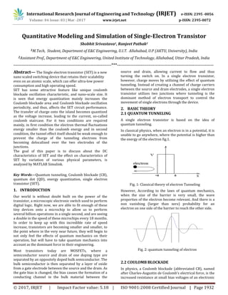
  • 1. International Research Journal of Engineering and Technology (IRJET) e-ISSN: 2395 -0056 Volume: 04 Issue: 03 | Mar -2017 www.irjet.net p-ISSN: 2395-0072 © 2017, IRJET | Impact Factor value: 5.18 | ISO 9001:2008 Certified Journal | Page 1932 Quantitative Modeling and Simulation of Single-Electron Transistor Shobhit Srivastava1, Ranjeet Pathak2 1M.Tech, Student, Department of E&C Engineering, U.I.T. Allahabad, U.P (AKTU, University), India 2Assistant Prof., Department of E&C Engineering, United Institute of Technology, Allahabad, Uttar Pradesh, India ------------------------------------------------------------------***----------------------------------------------------------------- Abstract— The Single electron transistor (SET) is a new nano scaled switching device that retains their scalability even on an atomic scale, which can offer ultra-low power consumption and high operating speed. SET has some attractive feature like unique coulomb blockade oscillation characteristic, and nano-scale size. It is seen that energy quantization mainly increases the Coulomb blockade area and Coulomb blockade oscillation periodicity, and thus, affects the SET circuit performance. The transfer of charge onto the island becomes quantized as the voltage increase, leading to the current, so-called coulomb staircase. For it two conditions are required mainly, in first condition the electron thermal fluctuations energy smaller than the coulomb energy and in second condition, the tunnel effect itself should be weak enough to prevent the charge of the tunneling electrons from becoming delocalized over the two electrodes of the junctions. The goal of this paper is to discuss about the DC characteristics of SET and the effect on characteristics of SET by variation of various physical parameters, is analyzed by MATLAB Simulink. Key Words—Quantum tunneling, Coulomb blockade (CB), quantum dot (QD), energy quantization, single electron transistor (SET). 1. INTRODUCTION Our world is without doubt built on the power of the transistor, a microscopic electronic switch used to perform digital logic. Right now, we are able to fit enough of these tiny devices onto a microchip to allow us to perform several billion operations in a single second, and are seeing a double in the speed of these microchips every 18 months. In order to keep up with this incredible rate of speed increase, transistors are becoming smaller and smaller, to the point where in the very near future, they will begin to not only feel the effects of quantum mechanics on their operation, but will have to take quantum mechanics into account as the dominant force in their engineering. Most transistors today are MOSFETs, where a semiconductor source and drain of one doping type are separated by an oppositely doped bulk semiconductor. The bulk semiconductor is then separated by a layer of oxide from a gate electrode between the source and the drain. As the gate bias is changed, the bias causes the formation of a conducting channel in the bulk material between the source and drain, allowing current to flow and thus turning the switch on. In a single electron transistor, however, charge moves by utilizing the effect of quantum tunneling. Instead of creating a channel of charge carriers between the source and drain electrodes, a single electron transistor utilizes two junctions where tunneling is the dominant method of electron transport to control the movement of single electrons through the device. 2. BASIC THEORY 2.1 QUANTUM TUNNELING A single electron transistor is based on the idea of quantum tunneling. In classical physics, when an electron is in a potential, it is unable to go anywhere, where the potential is higher than the energy of the electron fig.1. Fig. 1: Classical theory of electron Tunneling However, According to the laws of quantum mechanics, when the size of the barrier is very small, the wave properties of the electron become relevant. And there is a non vanishing (larger than zero) probability for an electron on one side of the barrier to reach the other side. Fig. 2: quantum tunneling of electron 2.2 COULOMB BLOCKADE In physics, a Coulomb blockade (abbreviated CB), named after Charles-Augustin de Coulomb's electrical force, is the increased resistance at small bias voltages of an electronic
  • 2. International Research Journal of Engineering and Technology (IRJET) e-ISSN: 2395 -0056 Volume: 04 Issue: 03 | Mar -2017 www.irjet.net p-ISSN: 2395-0072 © 2017, IRJET | Impact Factor value: 5.18 | ISO 9001:2008 Certified Journal | Page 1933 device comprising at least one low-capacitance tunnel junction. Because of the CB, the resistances of devices are not constant at low bias voltages, but increase to infinity for zero bias (i.e. no current flows). Due to the discreteness of electrical charge, current through a tunnel junction is a series of events in which exactly one electron passes (tunnels) through the tunnel barrier. The tunnel junction capacitor is charged with one elementary charge by the tunneling electron, causing a voltage buildup V= where e is the elementary charge of 1.6× coulomb and C the capacitance of the junction. If the capacitance is very small, the voltage buildup can be large enough to prevent another electron from tunneling. The electrical current is then suppressed at low bias voltages and the resistance of the device is no longer constant. The increase of the differential resistance around zero bias is called the Coulomb blockade. 2.3 CONDITION FOR COULOMB BLOCKED To achieve the Coulomb blockade, three criteria have to be met: The bias voltage must be lower than the elementary charge divided by the self capacitance of the island: V < (1) The thermal energy in the source contact and the thermal energy in the island must be below the charging energy or else the electron will be able to pass the QD via thermal excitation k T e c (2) The tunnelling resistance Rt, should be greater than h/e2 which is derived from Heisenberg’s uncertainty principle. h e (3) Rt 5813Ω The Coulomb energy is given by (4) Where e is the charge on an electron and is the total capacitance of the source and drain junctions and the gate capacitor. 2.4 SINGLE ELECTRON TRANSISTOR The simplest device, in which the effect of coulomb blockade can be observed, is the so-called single electron transistor. It consists of two electrodes known as the drain and the source, connected through tunnel junctions to one common electrode with a low self- capacitance known as the island. The electrical potential of the island can be tuned by a third electrode, known as the gate, capacitive coupled to the island, As shown in fig.3 Fig. 3: Single electron transistor Fig. 4: capacitance model for the SET 3. MODELING AND SIMULATION METHODOLOGY The Modeling and simulation of Single Electron Transistor is done using MATLAB Simulink. The SET circuit consisting of a dot between the source and drain electrodes separated by tunnel capacitors and . Both tunnel capacitors and have tunnel resistances and , respectively. The dot is also coupled to the gate electrode with capacitor in order to control the current flow. The total capacitance between the dot and the outer environment can be written as , where (5) Fig. 5: Equivalent circuit of SET There are four main equations for current-voltage characteristics of single electron circuits, i.e., free energy change ΔF, tunneling probability/rate ɼ, steady state master equation and current equation I as follows.
  • 3. International Research Journal of Engineering and Technology (IRJET) e-ISSN: 2395 -0056 Volume: 04 Issue: 03 | Mar -2017 www.irjet.net p-ISSN: 2395-0072 © 2017, IRJET | Impact Factor value: 5.18 | ISO 9001:2008 Certified Journal | Page 1934 3.1 Free energy change: ΔF1 (n1 n ) e * e ( e-Qo) ( g ) g g+ (6) ΔF (n1 n ) e e e-Qo 1 g g (7) Equations (6) and (7) are used to calculate the free (electrostatic) energy change ΔF of the system due to the one electron tunneling event. It is important to be noted that only tunneling events decreasing the electrostatic energy (and dissipating the difference) are possible. 3.2 Tunneling probability/rate: The most important requirement for occurrence of single electron tunneling is that the total energy of the system must Decrease due to one electron tunneling. Electron tunneling rate in tunnel junction ( ) can be calculated from derivation of Fermi Golden Rule. 1 R1e [ ΔF1 1- exp( ΔF1 kbT ) ] (8) 1 R e [ ΔF 1- exp( ΔF kbT ) ] (9) The values ΔF from equations (6) and (7) are used to calculate electron tunneling probability in the equations (8) and (9), respectively. The tunneling of a single electron through a particular tunnel junction is always a random event, with a certain rate (i.e., probability per unit time) which depends solely on the ΔF. 3.3 Steady State Master equation: p( ) - ( ) 1 ( ) p( 1) - ( 1) 1 ( 1) (10) ( ) e ∑ p- 1 ( ) – 1 - ( ) (11) e ∑ p- ( ) – - ( ) (12) Equation (10) expresses the Master equation in steady state, resulting the value of p (N), which is necessary to be used for the current calculation in equation (11) and (12). where e is the elemental charge, kb is the Boltzmann constant, T is the temperature, N is the number of electrons in the dot, n1 and n2 are a number of electrons flows through the capacitor C1 and capacitor C2, respectively, Qo is the background charge and +/- express that the electron tunnels through the capacitor with the direction from left to the right and from right to the left, respectively. The iterative algorithm of master equation method is presented in Figure Fig. 6: algorithm of master equation 4. FABRICATION PARAMETERS: The main fabrication parameters are source and drain tunnel junction capacitances, side gate capacitance, and control gate capacitance, are given below (13) Where Cg, Lg, Wch and Tgox are side gate capacitance, side gate length, channel width, and side gate oxide thickness respectively. (14) Where Cc, Lc, & Tcox are control gate capacitance, control gate length and control gate oxide thickness respectively. Before any electron tunneling, the tunneling junctions act as capacitances so it could be written as: (15) Where C1, C2, and Tsi are source capacitance, drain capacitance, and channel thickness, respectively .But here in this paper I only assume that SET is three terminal
  • 4. International Research Journal of Engineering and Technology (IRJET) e-ISSN: 2395 -0056 Volume: 04 Issue: 03 | Mar -2017 www.irjet.net p-ISSN: 2395-0072 © 2017, IRJET | Impact Factor value: 5.18 | ISO 9001:2008 Certified Journal | Page 1935 devices and neglect to Cc capacitance effect. Some external parameters (V ,Vg, T and qo) and some device parameters (C1, C2, Cg, R1 and R2), effects the properties of the SET but there is difference between them parameter like device parameter may be set before fabrication and external parameter may be adjust according to environmental condition given in below table 1 [9] Description Value Wch 15nm Lg 20nm Lc 10nm Tgox 10nm Tcox 5nm Tsi 15nm Table 1 Represents the approximate values of the parameters that is used for the fabrication of the silicon-based dual-gate SET [9]. 5. RESULT AND DISCUSSION The modeling of single electron transistor is based on its stability criteria for selecting parameters in such a way that all the characteristic of SET comes within the stability region, so below there is a brief discussion on stability and curve based on master’s equation of SET. 5.1 Stability plot for SET: The energy which determines electron transportation through a single-electron device is Helmholtz free energy which is defined as difference between total energy stored in the device and the work done by power source. Total energy stored includes all of energy components when an island is charged with an electron. For a SET with source and control gate terminals grounded, and drain and side gate terminals based at Vds and Vgs, the free energy has been formulated as following. (16) Here E is the electrostatic energy, Qg is the charge of the side gate capacitance, and Qd is the charge at drain tunnel junction capacitance. The change of Helmholtz free energy is calculated as: (17) Where Fi and Ff are the Helmholtz free energy of the system before and after an electron tunneling happens respectively. A tunneling could only happen if is negative. For a logic operation, i.e., where the number of electrons in the island is 0 or 1, is defined as: F ds ( 1⁄ ) gs ( g ⁄ ) (18) For the electron tunneling of the island to the source terminal is: F - ds ( 1⁄ ) - gs ( g ⁄ ) (19) If an electron tunnels from the island to the drain terminal, is defined as: ( ⁄ ) ( ⁄ ) (20) For the electron tunneling of the drain terminal to the island, F is: ( ⁄ ) ( ⁄ ) (21) The above equation (18-21) obtained from the equation 6 & 7. Now in SET, characteristic is known as stability plot. This plot is obtained by setting equations (18-21 equals to zero. Thus four lines’ equation will be obtained so that their cross creates a rhombus as shown below. Slop of these lines has been formulated as following: If electron tunnels from the island to the drain terminal and vice versa lines’ slope is: S1 ( g ) ⁄ (22) If electron tunnels from the source terminal to the island and vice versa lines’ slope is: g ⁄ (23) The stability plot of SET is illustrate in fig. (7)
  • 5. International Research Journal of Engineering and Technology (IRJET) e-ISSN: 2395 -0056 Volume: 04 Issue: 03 | Mar -2017 www.irjet.net p-ISSN: 2395-0072 © 2017, IRJET | Impact Factor value: 5.18 | ISO 9001:2008 Certified Journal | Page 1936 Fig.7. stability plot of SET for n=0 In this Figure the rhombus outside regions corresponds to regions with an integer number of the excess electrons on the island. In rhombus inside, there is no excess electron on the island (The Coulomb Blocked Region). But if charge will be present in this island region then stability criteria may be effected significantly, the stability region will be shifted in the right or left direction depend on the charge on the island, n = ..-2, -1 1 … as shown in figure 8. Here n=1, 2 represents number of electron in quantum dot, n=0 shows empty quantum dot and n=-1,-2 shows holes in quantum dot. Fig. 8 shift in stability region 5.2 Current oscillation on variation in Vgs For logic operation, if Vgs is increased and Vds is kept constant below the Coulomb blocked,| | , the current will oscillate with the period of Figure (9). This is because of Vds is not applied or increasing in accordance to pull the electron from source to QD to Drain for a continuous current. And thus Vgs is showing the control over transportation of electron from source to drain. Fig. 9. current oscillation with logical operation on Vgs Now to analysis the dc characteristic of SET, firstly it is assume that Vds may be zero or may have any fixed value. From equation 13-15, It is shown in Fig.10 that, by increase of the channel width, the Coulomb blockade region becomes narrower and the oscillation period of the drain current decreases. This is because by increase of the channel width, all capacitances change but the slope of S2 remains constant and the slope of S1 reduces, so rhombus inside area or the Coulomb blocked region decreases. In addition, the side gate capacitance decrease, therefore the oscillation period of the drain current decreases. Fig 10: Variation effect in the channel width on the Ids-Vgs Fig.11 shows the side gate length variation effect on the Ids-Vgs. It is demonstrated that, the increase of the side gate length causes the Coulomb blocked region to become narrower and the oscillation period of the drain current to become less. According to the equations (13-15), by increase of the side gate length, all capacitances are changed but the slope of S2 remains constant and the slope of S1 reduces, so the Coulomb blocked region decreases. The variation effect in the side gate length is less that the Variation effect in the channel width.
  • 6. International Research Journal of Engineering and Technology (IRJET) e-ISSN: 2395 -0056 Volume: 04 Issue: 03 | Mar -2017 www.irjet.net p-ISSN: 2395-0072 © 2017, IRJET | Impact Factor value: 5.18 | ISO 9001:2008 Certified Journal | Page 1937 Fig 11: Variation effect in the gate length on the Ids-Vgs It is demonstrated that, by increase of the side gate oxide thickness, the Coulomb blocked region becomes wider and the oscillation period of the drain current increases. According to equation 13-15, increase of this parameter causes the side gate capacitance to become less and the slope of both S1 and S2 to increase. Shown in fig12 Fig12: Variation effect in the gate oxide thickness on the Ids-Vgs Fig 13: Variation effect in temperature on the Ids-Vgs Above fig 13 demonstrates the temperature variation effect on the Ids-Vgs characteristic 5.3 Stair-Case Ids current For simulations purpose it is assumed that Vds is varied from -1v to 1v, T=20 K and assume gate voltage Vg=0 in case of Ids-Vds characteristic and assume Vg varied from -0.2v to 0.2v,Vds=18mv and T=2k . and from equation (11) and (12) we can plot Ids –Vds characteristic plot shows the device is symmetric. Fig.14. I–V characteristic plot. As shown as the coulomb staircase effect in Ids-Vds characteristic the may be too much effected by temperature variation as shown in Fig.15 Fig15: temperature variation effect on the Ids-Vds There is an increase in the value of current as temperature increases and there is also a very small difference in the value of the current when temperature becomes at high value range but there is all must reverse result will be obtained when increase in the value of background charges as shown in Fig.16
  • 7. International Research Journal of Engineering and Technology (IRJET) e-ISSN: 2395 -0056 Volume: 04 Issue: 03 | Mar -2017 www.irjet.net p-ISSN: 2395-0072 © 2017, IRJET | Impact Factor value: 5.18 | ISO 9001:2008 Certified Journal | Page 1938 Fig 16: Background charge variation effect on the Ids-Vds So this is good for SET Ids - Vds characteristic that there are no charges in the island. 6. CONCLUSION In conclusion, I have demonstrated the electrical characteristic of SET by using Master Equation approach and show a fairly accurate result with experimental data. Evidently, staircase pattern of I-V characteristic are clearly obtained as the main role of coulomb blockade effect in the SET system. This research paper focuses the theoretical discussion of basic principle of SET with importance of SET in the era of nanotechnology to provide low power consumption and high operating speed in the field of VLSI design for the fabrication of various electronic devices. SET has proved its value as tool in scientific research. The main problem in nanometer era is the fabrication of nano scale devices that can be achievable by the use of SET. 7. REFRENCES [1] Frans Willy and Yudi Darma, “Modeling and simulation of single electron transistor with master equation approach” 6th Asian Physics Symposium OP Publishing Journal of Physics: Conference Series 739 (2016) 012048 [2] Sheng Wang “Analytical Expressions and umerical simulation of single electron spectroscopy” Department of Physics, University of Science and Technology of China, Hefei, 230026, Sep 2013 [3] Surya Shankar Dan and Santanu Mahapatra, “Analysis of Energy Quantization Effects on Single-Electron Transistor Circuits” IEEE Transactions on nanotechnology, vol. 9, no. 1, January 2010 [4] Ahmed Shariful Alam, Abu Rena Md. Mustafa Kamal, Md. Nasmus Sakib Khan Shabbir, Atiqul Islam, “Single Electron Transistors (SET) substituting MOSFETs to Reduce Power Consumption of an nverter ircuit” nd Int'l Conf. on Electrical Engineering and Information & Communication Technology (ICEEICT) 2015 [5] Vinay Pratap Singh, Arun Agrawal, Shyam Babu Singh, “Analytical Discussion of Single Electron Transistor (SET), International Journal of Soft Computing and Engineering (IJSCE) ISSN: 2231-2307, Volume-2, Issue-3, July 2012 [6] K.Miyaji, M. Saitoh and T. Hiramoto “ ompact analytical model for room- temperature operating silicon single-electron transistors with discrete quantum levels”, IEEE Trans. Nanotechnology, vol. 5, May 2006. [7] A. Boubaker, M. Troudi , “A spice model for single electron transistor applications at low temperatures: inverter and ring oscillator” nternational Conference on Design & Technology of Integrated Systems in Nano scale Era, 2008 [8] Pankaj Kumar Sinha and Sanjay S “Single Electron Transistor and its Simulation methods” nternational Journal of Engineering Development and Research (IJEDR) 2014 | Volume 2, Issue 2 | ISSN: 2321-9939 [9] Khadijeh Feizi, Saeed Haji Nasiri, “DC Characteristic Analysis of Single-Electron Transistor Based on MIB Model”, International Conference on Nanotechnology and Biosensors (2011) IACSIT Press, Singapore 8. BIOGRAPHIES Shobhit Srivastava, born in Varanasi, U.P., India, on June 22, 1990. He received the B.Tech. degree in E&C Engineering from UPTU University, UP, India in 2011 and Pursuing M.Tech from the Department of E&C Engineering, from Dr. A.P.J. Abdul Kalam Technical University, UP, India. His current research interests include device reliability, modelling, optimization and design of integrated circuits for Nano Technology.