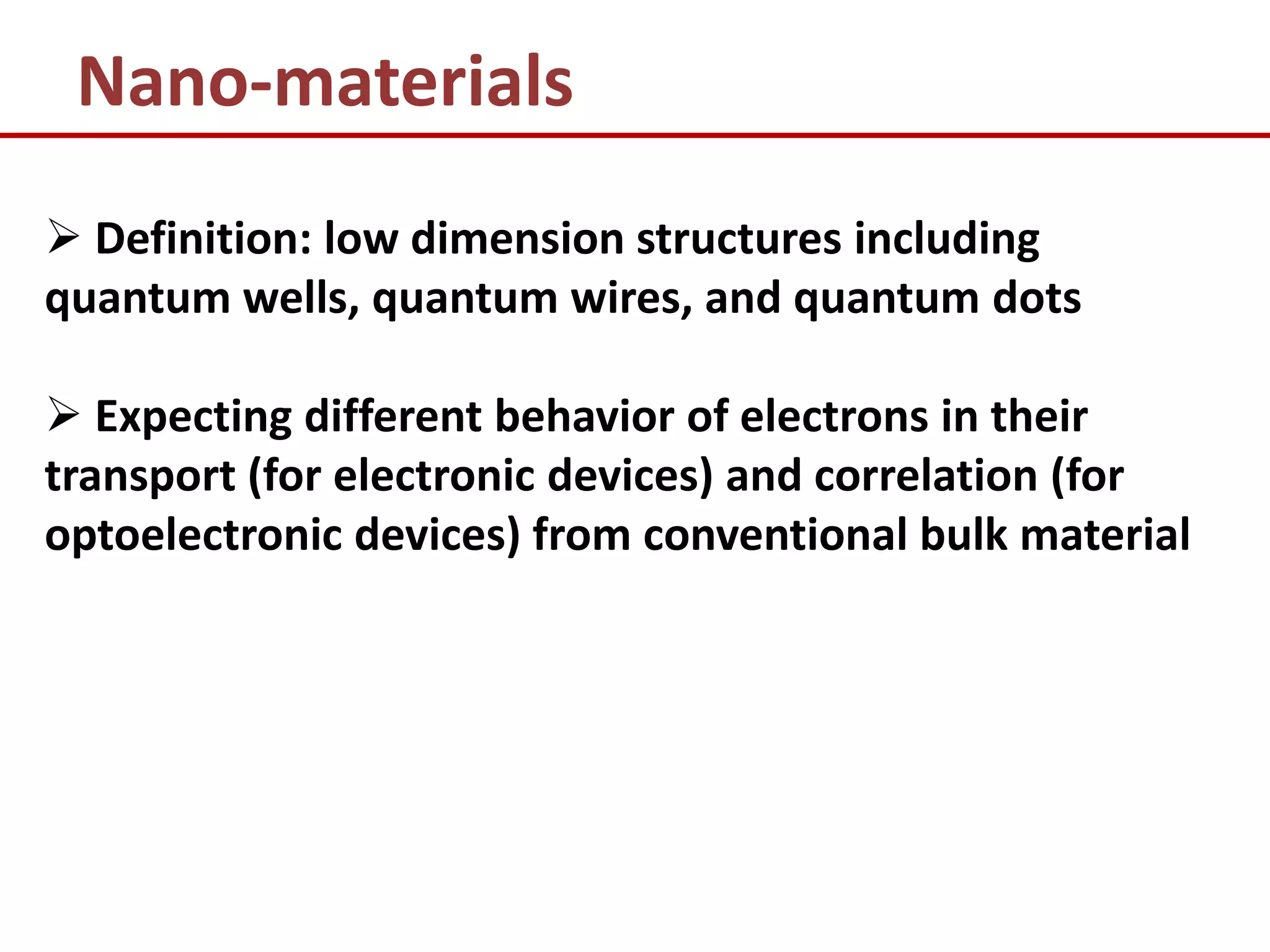
An Introduction to Nano-Science
        & Nano-Technology


Dr. Abdul Waheed Anwar
        Nanotechnology Research Center
        Department of Physics
        UET Lahore
Nano-materials

 What is “nano-material” and why we are
interested in it?

 Optical and electronic properties of nano-
materials
Nano-materials
 Definition: low dimension structures including
quantum wells, quantum wires, and quantum dots

 Expecting different behavior of electrons in their
transport (for electronic devices) and correlation (for
optoelectronic devices) from conventional bulk material
Nano-materials
Electron behavior:

Quantum well – 1D confined and in parallel plane 2D Bloch
  wave

Quantum wire – in cross-sectional plane 2D confined and 1D
  Bloch wave

Quantum dot – all 3D confined
Nano-materials


Bulk semiconductor
   – plane wave like with effective mass, two different type
      of electrons identified with opposite sign of their
      effective mass, i.e., electrons and holes

   – parabolic band dispersion (E~k) relation

   – density of states in terms of E: continues square root
     dependence, with different parameters for
     electrons/holes in different band
Nano-materials
• Quantum well
   – discrete energy levels in 1D for both electrons and holes
   – different effective masses in 2D parallel plane for electrons and holes
   – dispersion (E~k) relation: parabolic bands with discrete states inside the stop-
     band
   – density of states in terms of E: additive staircase functions, with different
     parameters for electrons/holes in different band

• Quantum wire
   – discrete energy levels in 2D cross-sectional plane for both electrons and holes
   – different effective masses in 1D for electrons and holes
   – dispersion (E~k) relation: parabolic bands with discrete states inside the stop-
     band
   – density of states in terms of E: additive staircase decayed functions, with
     different parameters for electrons/holes in different band
Nano-materials


• Quantum dot
   – discrete energy levels for both electrons and holes
   – discrete energy states only
   – density of states in terms of E: -functions for
     electrons/holes
Nano-materials

 Electrons in semiconductors: easily controllable and
  accessible

 Electrons in atomic systems: hardly controllable or
  accessible
Nano-materials

   Geometrical dimensions in the artificial structure
  can be tuned to change the confinement of electrons
  and holes, hence to tailor the correlations (e.g.,
  excitations, transitions and recombinations)
   The reduced probability of inelastic and elastic
  collisions (much expected for quantum computing,
  could be a drawback for light emitting devices)
   Definite polarization (spin of photons are regulated)
  (Coulomb) binding between electron and hole is
  increased due to the localization
Nano-materials
• Current technologies
  – Top-down approach: patterning  etching  re-
    growth
  – Bottom-top approach: patterning  etching 
    selective-growth
  – Uneven substrate growth: edge overgrowth, V-
    shape growth, interface QD, etc.
  – Self-organized growth: most successful approach
    so far
Carbon Nanotubes
Carbon nanotubes: an important 1-D
material in Nanoscience and nanotechnology
with exceptional properties such as

 Properties           SWNT          Comparison
 Very low density     1.33-1.44     Al 2.7g/cm3
                      g/cm3
 High tensile         Upto 63 GPa   Steel <2GPa
 strength
 High current         ≈109 A/cm2    Cu <106 A/cm2
 density
 Excellent heat       ≈ 4000 W/mK   Diamond ≈ 4000
 transmission                       W/mK
 Strong temperature   Upto 2800 oC Metal in
 stability            in vaccum    μchips <1000 oC
Carbon Nanotubes

Wide range of applications:
   Molecular Electronics
   Fibres and Fabrics
   Conductive Plastics
   Field Emission
   Conductive Adhesives
   Sensors               DNA-Functionalized
   Thermal Materials     CNT-FET for
   Medical diagnostic    Chemical Sensing
   medical treatment      Cristian Staii et al, Nano Letters, 5, 1774 (2005)
Carbon Nanotubes
    CNT is a tubular form of two dimensional
    graphene


                               Zigzag   (n1,0)
                               Armchair (n1,n1)
 Chiral indices n1(4),n2(2)   Chiral   (n1,n2)

 Chiral vector Ch=n1a1+n2a2
 Chiral angle θ: between Ch and a1
Carbon Nanotubes
      SWCNT                                                        MWCNT
      diameter : 1.2 nm


  http://www.almaden.ibm.com/st/past_projects/nanotubes/?page3     http://www.nano-lab.com/nanotube-image3.html


         DWCNT                                                   DWCNT
                                                                  CCVD
                                                                  Peapods C60@SWCNT
                                                                  Arc Discharge

 Nanoscience and Technology,2005,Part III,203-224
Carbon Nanotubes

                                           C1
     Metallic SWCNT
                                      M           Constant DOS at
                                     E11           Fermi level
                                           V1


Semiconducting SWCNT                       C1    SC
                                                E11   Zero DOS at
                                           V1         Fermi level


         The band structure   Densities of states

SWCNT Optical properties depend on the
allowed electronic transitions between van
Hove singularities (vHs)
Carbon Nanotubes
  Metallic                    :(n1-n2)mod3=0
  Semiconducting:(n1-n2)mod3=1
                    or
                :(n1-n2)mod3=2


    SWCNT optoelectronic
    properties depend on
    chiral indices & diameter
www.sustainability.rit.edu/nanopower/rcn.html
Gold, Silver and Platinum Nano-materials


 Metals are unique in their physical and chemical
properties as compared to other compound materials
such as metal oxides, sulphides and nitrides.

 Metals have ductility, malleability, luster, high
density, fewer defects and are generally crystalline in
nature.
Gold, Silver and Platinum Nano-materials
Nano-materials


Gold is one of the few metallic elements that can be used in
nano scale system and devices due to its resistance to
oxidation.

More over gold has some additional properties at nano scale
Gold, Silver and Platinum Nano-materials

 The coloring nature of Au and Ag nano-particles was
 fundamental identification for their nano-particle colloid
 formation.

 Making use of this, they have been used as coloring
 agents in decorative glasses and clothing.

 This is due to light-absorbing nature of the
 surface of Au and Ag nano-particles because of the surface
 plasmon resonance.
What Is Nano?

 Pt nano-particles are catalytically active for oxidation and
reduction reactions.

 As a result, these nano-materials find applications for catalytic
use.

 Since Au, Ag and Pt nano-particles have considerable stability
as compared to other metals, they have gained importance.

However, in the near future, all metals will be possibly shaped
in nano size by using suitable stabilizing agents and medium.
Electronic Properties
• Ballistic transport – a result of much reduced
  electron-phonon scattering, low temperature
  mobility in QW (in-plane direction) reaches a rather
  absurd value ~107cm2/s-V, with corresponding mean
  free path over 100m

• Resulted effect – electrons can be steered, deflected
  and focused in a manner very similar to optics, as an
  example, Young’s double slit diffraction was
  demonstrated on such platform
Electronic Properties
• If excitation (charging) itself is also quantized
  (through, e.g., Coulomb blockade), interaction
  between the excitation quantization and the
  quantized eigen states (i.e., the discrete energy levels
  in nano-structure) brings us into a completely
  discrete regime

• Resulted effect – a possible platform to manipulate
  single electron to realize various functionalities, e.g.,
  single electron transistor (SET) for logical gate or
  memory cell
Optical Properties

• Discretization of energy levels increases the density
  of states

• Resulted effect – enhances narrow band correlation,
  such as electron-hole recombination.
Optical Properties

• Discretization of energy levels reduces broadband
  correlation

• Resulted effect –reduces temperature dependence;
  which is very much needed in quantum computing
  and reduces device performance temperature
  dependence
Optical Properties

• Quantized energy level dependence on size
  (geometric dimension)

• Resulted effect – tuning of optical gain/absorption
  spectrum
Quantum Dot
Quantum dots are semiconductor very small nano
crystalswhich can be considered as dimensionless.

Quantum dots range from 2-10 nanometers (10-50 nm) in
diameters

An exciton pair is defined as an electron and hole pair.

An exciton Bohr radius is the distance in an electron hole
pair

 The size of QD is of the same order as the radius of exciton
Bohr radius
What Is Nano?

Nano Tech Lecture2 Dr. A. Waheed Anwar

  • 1.
    An Introduction toNano-Science & Nano-Technology Dr. Abdul Waheed Anwar Nanotechnology Research Center Department of Physics UET Lahore
  • 2.
    Nano-materials  What is“nano-material” and why we are interested in it?  Optical and electronic properties of nano- materials
  • 3.
    Nano-materials  Definition: lowdimension structures including quantum wells, quantum wires, and quantum dots  Expecting different behavior of electrons in their transport (for electronic devices) and correlation (for optoelectronic devices) from conventional bulk material
  • 4.
    Nano-materials Electron behavior: Quantum well– 1D confined and in parallel plane 2D Bloch wave Quantum wire – in cross-sectional plane 2D confined and 1D Bloch wave Quantum dot – all 3D confined
  • 5.
    Nano-materials Bulk semiconductor – plane wave like with effective mass, two different type of electrons identified with opposite sign of their effective mass, i.e., electrons and holes – parabolic band dispersion (E~k) relation – density of states in terms of E: continues square root dependence, with different parameters for electrons/holes in different band
  • 6.
    Nano-materials • Quantum well – discrete energy levels in 1D for both electrons and holes – different effective masses in 2D parallel plane for electrons and holes – dispersion (E~k) relation: parabolic bands with discrete states inside the stop- band – density of states in terms of E: additive staircase functions, with different parameters for electrons/holes in different band • Quantum wire – discrete energy levels in 2D cross-sectional plane for both electrons and holes – different effective masses in 1D for electrons and holes – dispersion (E~k) relation: parabolic bands with discrete states inside the stop- band – density of states in terms of E: additive staircase decayed functions, with different parameters for electrons/holes in different band
  • 7.
    Nano-materials • Quantum dot – discrete energy levels for both electrons and holes – discrete energy states only – density of states in terms of E: -functions for electrons/holes
  • 8.
    Nano-materials  Electrons insemiconductors: easily controllable and accessible  Electrons in atomic systems: hardly controllable or accessible
  • 9.
    Nano-materials Geometrical dimensions in the artificial structure can be tuned to change the confinement of electrons and holes, hence to tailor the correlations (e.g., excitations, transitions and recombinations)  The reduced probability of inelastic and elastic collisions (much expected for quantum computing, could be a drawback for light emitting devices)  Definite polarization (spin of photons are regulated) (Coulomb) binding between electron and hole is increased due to the localization
  • 10.
    Nano-materials • Current technologies – Top-down approach: patterning  etching  re- growth – Bottom-top approach: patterning  etching  selective-growth – Uneven substrate growth: edge overgrowth, V- shape growth, interface QD, etc. – Self-organized growth: most successful approach so far
  • 11.
    Carbon Nanotubes Carbon nanotubes:an important 1-D material in Nanoscience and nanotechnology with exceptional properties such as Properties SWNT Comparison Very low density 1.33-1.44 Al 2.7g/cm3 g/cm3 High tensile Upto 63 GPa Steel <2GPa strength High current ≈109 A/cm2 Cu <106 A/cm2 density Excellent heat ≈ 4000 W/mK Diamond ≈ 4000 transmission W/mK Strong temperature Upto 2800 oC Metal in stability in vaccum μchips <1000 oC
  • 12.
    Carbon Nanotubes Wide rangeof applications:  Molecular Electronics  Fibres and Fabrics  Conductive Plastics  Field Emission  Conductive Adhesives  Sensors DNA-Functionalized  Thermal Materials CNT-FET for  Medical diagnostic Chemical Sensing  medical treatment Cristian Staii et al, Nano Letters, 5, 1774 (2005)
  • 13.
    Carbon Nanotubes CNT is a tubular form of two dimensional graphene Zigzag (n1,0) Armchair (n1,n1)  Chiral indices n1(4),n2(2) Chiral (n1,n2)  Chiral vector Ch=n1a1+n2a2  Chiral angle θ: between Ch and a1
  • 14.
    Carbon Nanotubes SWCNT MWCNT diameter : 1.2 nm http://www.almaden.ibm.com/st/past_projects/nanotubes/?page3 http://www.nano-lab.com/nanotube-image3.html DWCNT DWCNT  CCVD  Peapods C60@SWCNT  Arc Discharge Nanoscience and Technology,2005,Part III,203-224
  • 15.
    Carbon Nanotubes C1 Metallic SWCNT M Constant DOS at E11 Fermi level V1 Semiconducting SWCNT C1 SC E11 Zero DOS at V1 Fermi level The band structure Densities of states SWCNT Optical properties depend on the allowed electronic transitions between van Hove singularities (vHs)
  • 16.
    Carbon Nanotubes Metallic :(n1-n2)mod3=0 Semiconducting:(n1-n2)mod3=1 or :(n1-n2)mod3=2 SWCNT optoelectronic properties depend on chiral indices & diameter www.sustainability.rit.edu/nanopower/rcn.html
  • 17.
    Gold, Silver andPlatinum Nano-materials  Metals are unique in their physical and chemical properties as compared to other compound materials such as metal oxides, sulphides and nitrides.  Metals have ductility, malleability, luster, high density, fewer defects and are generally crystalline in nature.
  • 18.
    Gold, Silver andPlatinum Nano-materials
  • 19.
    Nano-materials Gold is oneof the few metallic elements that can be used in nano scale system and devices due to its resistance to oxidation. More over gold has some additional properties at nano scale
  • 20.
    Gold, Silver andPlatinum Nano-materials The coloring nature of Au and Ag nano-particles was fundamental identification for their nano-particle colloid formation. Making use of this, they have been used as coloring agents in decorative glasses and clothing. This is due to light-absorbing nature of the surface of Au and Ag nano-particles because of the surface plasmon resonance.
  • 21.
    What Is Nano? Pt nano-particles are catalytically active for oxidation and reduction reactions.  As a result, these nano-materials find applications for catalytic use.  Since Au, Ag and Pt nano-particles have considerable stability as compared to other metals, they have gained importance. However, in the near future, all metals will be possibly shaped in nano size by using suitable stabilizing agents and medium.
  • 22.
    Electronic Properties • Ballistictransport – a result of much reduced electron-phonon scattering, low temperature mobility in QW (in-plane direction) reaches a rather absurd value ~107cm2/s-V, with corresponding mean free path over 100m • Resulted effect – electrons can be steered, deflected and focused in a manner very similar to optics, as an example, Young’s double slit diffraction was demonstrated on such platform
  • 23.
    Electronic Properties • Ifexcitation (charging) itself is also quantized (through, e.g., Coulomb blockade), interaction between the excitation quantization and the quantized eigen states (i.e., the discrete energy levels in nano-structure) brings us into a completely discrete regime • Resulted effect – a possible platform to manipulate single electron to realize various functionalities, e.g., single electron transistor (SET) for logical gate or memory cell
  • 24.
    Optical Properties • Discretizationof energy levels increases the density of states • Resulted effect – enhances narrow band correlation, such as electron-hole recombination.
  • 25.
    Optical Properties • Discretizationof energy levels reduces broadband correlation • Resulted effect –reduces temperature dependence; which is very much needed in quantum computing and reduces device performance temperature dependence
  • 26.
    Optical Properties • Quantizedenergy level dependence on size (geometric dimension) • Resulted effect – tuning of optical gain/absorption spectrum
  • 27.
    Quantum Dot Quantum dotsare semiconductor very small nano crystalswhich can be considered as dimensionless. Quantum dots range from 2-10 nanometers (10-50 nm) in diameters An exciton pair is defined as an electron and hole pair. An exciton Bohr radius is the distance in an electron hole pair  The size of QD is of the same order as the radius of exciton Bohr radius
  • 28.