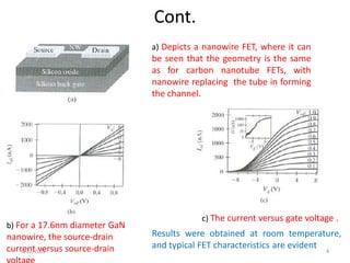
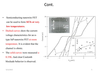
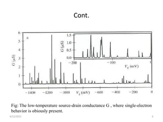
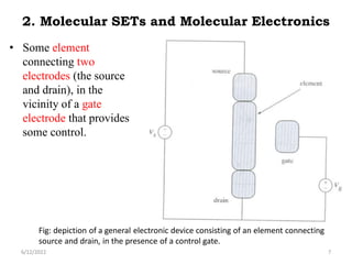
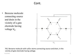
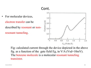
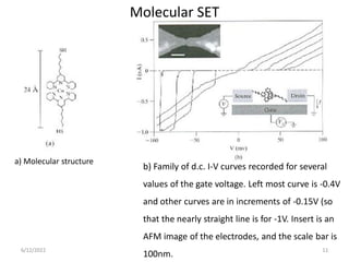
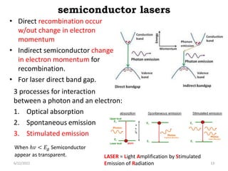
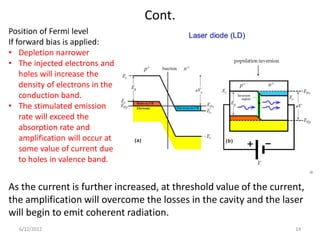
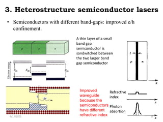
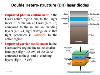
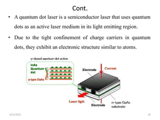
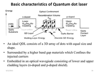
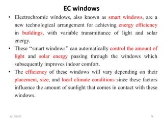
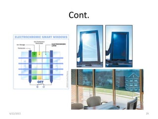
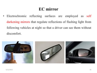
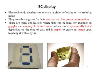
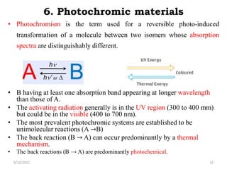
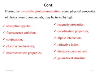
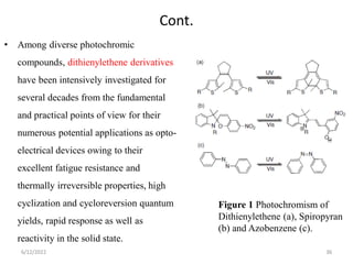
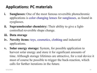
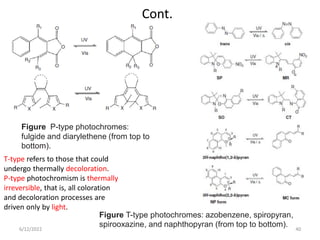
The principles of physics, as far as I can see, do not speak
against the possibility of maneuvering things atom by atom.”
“Put the atoms down where the chemist says, and so you make
the substance.”
in this ppt it was explained that the importance of dssc and the working principles and the notes during the research work..
the concept was explained in the ppt was very clear......
The document summarizes key information about optical sources used for fiber optic communications. It describes how semiconductor laser diodes and light-emitting diodes (LEDs) use a pn junction to emit light via radiative recombination of electrons and holes. LEDs emit incoherent light, while laser diodes emit coherent light confined within an optical cavity. The document discusses characteristics of LEDs and laser diodes, including their structures, materials used, emission properties, and applications in optical communication systems.
Auger Electron Spectroscopy (AES) uses a focused electron beam to eject inner shell electrons from the surface of a sample. The vacancies are filled by higher-energy electrons, emitting characteristic "Auger electrons" that can be analyzed to determine the elemental composition of the top few atomic layers. The key components of an AES system are an electron gun, electron energy analyzer, electron detector, and ultra-high vacuum environment. AES provides surface sensitivity, elemental analysis, and depth profiling capabilities. Limitations include inability to analyze non-conductive samples and lack of hydrogen/helium detection.
This document provides an overview of the 3C3 - Analogue Circuits course taught at Trinity College Dublin. It includes information about assessment, module details, reading materials, lecture and tutorial times, and the course outline. The course outline lists topics that will be covered such as physical operation of transistors, amplifier configurations, filters, and oscillators. It provides subtopics for some of the main topics as well. The document aims to give students an introduction to the course and what will be covered over the semester.
This document introduces nano-materials and discusses their properties and applications. It defines nano-materials as low-dimensional semiconductor structures between a few nanometers to tens of nanometers in size, including quantum wells, wires, and dots. Electron behavior changes from plane waves in bulk semiconductors to quantized energy levels in nano-structures. Nano-materials are of interest because they combine advantages of semiconductors and atomic systems by allowing controllable electron confinement. Common fabrication methods include top-down patterning and bottom-up self-assembly. Nano-materials exhibit properties like ballistic transport, tunneling, and discrete optical transitions useful for applications in lasers, detectors, and other optoelectronic devices
This document provides an introduction to nano-materials. It defines nano-materials as artificial semiconductor structures with dimensions on the nanometer scale, including quantum wells, wires, and dots. Electron behavior changes from plane waves in free space, to Bloch waves in bulk semiconductors, to discrete energy levels in low-dimensional nano-structures. Nano-materials are of interest because they allow tailoring of electronic and optical properties by controlling geometric confinement. Common fabrication methods include lithography and self-organized growth to achieve sizes less than 100nm for full quantum confinement effects. Nano-materials demonstrate properties like ballistic transport, tunneling, and quantized energy levels that enable applications in light sources, detectors, and electronic devices
Semiconductors have properties between conductors and insulators that make them useful for various applications. Their conductivity can be modified through doping with impurities. Thermistors use semiconductors whose resistivity varies with temperature, allowing them to act as thermometers. Hall probes measure magnetic fields by detecting the Hall voltage induced in a semiconductor. Semiconductors are the foundation of modern electronics due to their ability to amplify or switch electrical signals through doping or interaction with electric fields or light.
This document provides information about the course EEE111 Analog Electronics offered in the spring 2023 semester. It includes details like the course code, title, semester, instructor's name and contact information. The document outlines the topics that will be covered, such as semiconductor devices, diodes, transistors, and electronic circuits. It lists the course objectives, outcomes, assessment methods including exams, quizzes, assignments and laboratory work. Recommended textbooks and references are also provided.
The document provides information about spintronics, which is an emerging field that utilizes the spin of electrons rather than just their charge. It discusses how spintronics works on the principle of manipulating the spin of electrons using magnetic fields, offering advantages like non-volatility and low power. Key effects and devices in spintronics discussed include giant magnetoresistance, spin valves, magnetic random access memory, spin transistors, and tunnel magnetoresistance. The document also outlines some applications of spintronics, advantages over conventional electronics, current limitations, and future demands and directions for the field.
Electron Beam Lithography review paper - EE541 Dublin City UniversityRay Tyndall
Electron beam lithography (EBL) uses a focused beam of electrons to pattern nanostructures onto a resist. EBL can produce features smaller than 10nm. High energy electrons (10-100keV) are focused into a narrow beam and used to expose regions on an electron-sensitive resist. The resolution is limited by electron scattering within the resist and substrate, which causes the exposed area to be larger than the beam size. EBL is widely used in semiconductor manufacturing for patterning at the nanoscale but proximity effects from electron scattering make it challenging to produce small, dense features. Techniques such as higher beam voltages, dose modulation, and multiple resist layers help overcome these limitations.
The attached narrated power point presentation mentions the different types of optical sources used for optical fiber communications, the requirements for light sources for optical fiber communications, direct and indirect bandgap semiconductors and different types of LEDs in use today along with their comparison. The material will be useful for KTU final year B Tech students who prepare for the subject EC 405, Optical Communications.
Dielectric materials are insulators that can store electrical energy through polarization. They are used widely in applications like capacitors, transformers, and insulation. Dielectrics are characterized by their dielectric constant, which measures their ability to store charge when polarized by an electric field. The polarization of dielectrics occurs through mechanisms like electronic, ionic, and orientational polarization that create dipole moments in the material. The properties of dielectric materials, including their dielectric constant, are dependent on factors like frequency and temperature of an applied electric field.
This document discusses wireless power transfer technologies and their application to LED lighting systems. It begins with an introduction to wireless power transfer and wireless-driven LED systems. It then provides background on the history of wireless power by discussing Nikola Tesla's Tesla coil experiments. The document outlines four main methods of wireless power transfer: electromagnetic induction, capacitive coupling, resonant inductive coupling, and microwave transmission. It also discusses LEDs and their advantages for lighting. The document concludes that wireless power techniques have opportunities to make LED products more convenient and reliable compared to traditional wired systems.
Supercapacitor materials were presented. Supercapacitors store electrical energy at the interface between an electrode and electrolyte through ion adsorption, unlike batteries which store chemical energy. They have higher power density than batteries and higher energy density than conventional capacitors. Common electrode materials include activated carbon, graphene, metal oxides like ruthenium oxide and nickel oxide, and conducting polymers. Supercapacitors can be used in applications requiring bursts of energy like regenerative braking and have a longer lifespan than batteries. Future work aims to improve capacitance and energy density through nanocomposite electrodes.
The document provides information on Electrical Discharge Machining (EDM). EDM is a manufacturing process where electrical discharges are used to erode material from a workpiece to achieve a desired shape. In EDM, a series of sparks erode material by rapidly recurring electrical discharges between two electrodes separated by a dielectric liquid and subject to an electric voltage. One electrode is the tool that shapes the workpiece. Material removal occurs through thermal melting and vaporization caused by the extreme heat of electrical sparks between the electrodes.
Electrochemical Impedance Spectroscopy.pptxJahanzeb Ahmad
1) Electrochemical Impedance Spectroscopy (EIS) is a powerful method to analyze the complex electrical resistance of a system. It has been widely applied to study electrochemical properties like charge transport, electrode kinetics, and double layer studies.
2) EIS measurements involve applying a small AC potential signal over a range of frequencies and measuring the impedance response. Electrochemical cells can be modeled as equivalent electrical circuits containing elements like electrolyte resistance, double layer capacitance, charge transfer resistance, and Warburg impedance.
3) A case study showed that immobilizing an antibody on a modified electrode led to an increase in charge transfer resistance and decrease in peak current, confirming successful surface immobilization. E
Semiconductors have electrical properties between conductors and insulators. They behave as insulators at low temperatures but conduct electricity at room temperature due to their small band gap. Doping semiconductors with impurities creates an excess of electrons or holes, making them n-type or p-type. A p-n junction is formed at the boundary between p-type and n-type semiconductors and allows current to flow in only one direction, making it useful for diodes. Diodes are used to convert alternating current to direct current and have many applications in electronics.
Electrical Discharge Machining (EDM) is a manufacturing process where electrical discharges are used to erode material from a workpiece to achieve a desired shape. In EDM, a potential difference is applied between an electrode tool and the workpiece, which are separated by a dielectric liquid. This causes electric sparks to form that melt and vaporize small amounts of material from both the tool and workpiece. Kerosene or deionized water is typically used as the dielectric liquid to facilitate flushing of debris and prevent oxidation during the process.
Electrical Discharge Machining (EDM) is a manufacturing process where electrical discharges are used to erode material from a workpiece to achieve a desired shape. In EDM, a series of electrical sparks are generated between two electrodes submerged in a dielectric liquid and subject to an electric voltage. This causes material to be removed from both electrodes through localized melting and vaporization due to the extreme heat of the sparks. EDM can be used to machine hard metals and intricate shapes that would be difficult to machine through conventional methods.
This document provides information about a course on semiconductor devices, including bipolar junction transistors (BJTs). It lists the course aims as reviewing diode and BJT operation, extending knowledge to include recombination influences, investigating speed limitations, and extracting equivalent circuit models. It recommends textbooks and outlines the course topics as reviewing semiconductor devices and pn diodes, studying long pn diodes incorporating recombination, examining BJT DC operation and switching characteristics, and why studying devices is important.
The document discusses using light instead of electricity for digital logic circuits to overcome limitations of miniaturized electronic systems. It proposes that optical switching speeds could exceed electrical switching and have very low power consumption. Photonic crystals that selectively allow or block wavelengths could be used to efficiently channel and manipulate light for all-optical digital devices. Specifically, electro-optic devices have been made using opals and inverse opals that can tune photonic crystals by changing their behavior in an electric field, and all-optical circuits could theoretically operate faster than electro-optic circuits since they would not require converting between light and electricity.
A Hybrid Model to Predict Electron and Ion Distributions in Entire Interelect...Fa-Gung Fan
Atmospheric direct current (dc) corona discharge
from thin wires or sharp needles has been widely used as an ion
source in many devices such as photocopiers, laser printers, and
electronic air cleaners. Existing numerical models to predict the
electron distribution in the corona plasma are based on charge
continuity equations and the simplified Boltzmann equation. In
this paper, negative dc corona discharges produced from a thin
wire in dry air are modeled using a hybrid model of modified
particle-in-cell plus Monte Carlo collision (PIC-MCC) and a
continuum approach. The PIC-MCC model predicts densities of
charge carriers and electron kinetic energy distributions in the
plasma region, while the continuum model predicts the densities of
charge carriers in the unipolar ion region. Results from the hybrid
model are compared with those from prior continuum models.
Superior to the prior continuum model, the hybrid model is able
to predict the voltage–current curve of corona discharges. The
PIC-MCC simulation results also suggest the validity of the local
approximation used to solve the Boltzmann equation in the prior
continuum model.
This presentation, created by Syed Faiz ul Hassan, explores the profound influence of media on public perception and behavior. It delves into the evolution of media from oral traditions to modern digital and social media platforms. Key topics include the role of media in information propagation, socialization, crisis awareness, globalization, and education. The presentation also examines media influence through agenda setting, propaganda, and manipulative techniques used by advertisers and marketers. Furthermore, it highlights the impact of surveillance enabled by media technologies on personal behavior and preferences. Through this comprehensive overview, the presentation aims to shed light on how media shapes collective consciousness and public opinion.
This presentation by Professor Alex Robson, Deputy Chair of Australia’s Productivity Commission, was made during the discussion “Competition and Regulation in Professions and Occupations” held at the 77th meeting of the OECD Working Party No. 2 on Competition and Regulation on 10 June 2024. More papers and presentations on the topic can be found at oe.cd/crps.
This presentation was uploaded with the author’s consent.
XP 2024 presentation: A New Look to Leadershipsamililja
Presentation slides from XP2024 conference, Bolzano IT. The slides describe a new view to leadership and combines it with anthro-complexity (aka cynefin).
Collapsing Narratives: Exploring Non-Linearity • a micro report by Rosie WellsRosie Wells
Insight: In a landscape where traditional narrative structures are giving way to fragmented and non-linear forms of storytelling, there lies immense potential for creativity and exploration.
'Collapsing Narratives: Exploring Non-Linearity' is a micro report from Rosie Wells.
Rosie Wells is an Arts & Cultural Strategist uniquely positioned at the intersection of grassroots and mainstream storytelling.
Their work is focused on developing meaningful and lasting connections that can drive social change.
Please download this presentation to enjoy the hyperlinks!
Mastering the Concepts Tested in the Databricks Certified Data Engineer Assoc...SkillCertProExams
• For a full set of 760+ questions. Go to
https://skillcertpro.com/product/databricks-certified-data-engineer-associate-exam-questions/
• SkillCertPro offers detailed explanations to each question which helps to understand the concepts better.
• It is recommended to score above 85% in SkillCertPro exams before attempting a real exam.
• SkillCertPro updates exam questions every 2 weeks.
• You will get life time access and life time free updates
• SkillCertPro assures 100% pass guarantee in first attempt.
Suzanne Lagerweij - Influence Without Power - Why Empathy is Your Best Friend...Suzanne Lagerweij
This is a workshop about communication and collaboration. We will experience how we can analyze the reasons for resistance to change (exercise 1) and practice how to improve our conversation style and be more in control and effective in the way we communicate (exercise 2).
This session will use Dave Gray’s Empathy Mapping, Argyris’ Ladder of Inference and The Four Rs from Agile Conversations (Squirrel and Fredrick).
Abstract:
Let’s talk about powerful conversations! We all know how to lead a constructive conversation, right? Then why is it so difficult to have those conversations with people at work, especially those in powerful positions that show resistance to change?
Learning to control and direct conversations takes understanding and practice.
We can combine our innate empathy with our analytical skills to gain a deeper understanding of complex situations at work. Join this session to learn how to prepare for difficult conversations and how to improve our agile conversations in order to be more influential without power. We will use Dave Gray’s Empathy Mapping, Argyris’ Ladder of Inference and The Four Rs from Agile Conversations (Squirrel and Fredrick).
In the session you will experience how preparing and reflecting on your conversation can help you be more influential at work. You will learn how to communicate more effectively with the people needed to achieve positive change. You will leave with a self-revised version of a difficult conversation and a practical model to use when you get back to work.
Come learn more on how to become a real influencer!
2. Topics:
1. Semiconductor Nanowire FETs and SETs
2. Molecular SETs and Molecular Electronics
3. Heterostructure semiconductor lasers
4. Quantum dot lasers
5. Electrochromic Materials
• Optical effects and quantification of colour
• Electrochromic Systems: Electrochemistry, Kinetics and Mechanism
• Construction of Electrochromic Devices
• Electrochromic Systems (Inorganic Systems/ organic Systems)
• Applications of electrochromic devices
6. Photochromic materials
• Fundamentals of Photochromic materials
• Organic Photochromic Molecules
• Multi-addressable Photochromic Materials
• Photoswitchable Supramolecular Systems
• Photochromic Bulk Materials
• Industrial Applications and Perspectives of Photochromic
materials
6/12/2022 2
3. 1. Semiconductor Nanowire FETs and SETs
• Semiconducting nanowires can serve as FETs and SETs
channels.
• Semiconducting nanowires typically have diameters in the
range 10-100nm and controlled growth can result in nanowires
that are quite and straight, with few defects.
• Both p- and n- type nanowires can be fabricated, and a variety
of devices have been demonstrated.
6/12/2022 3
4. Cont.
a) Depicts a nanowire FET, where it can
be seen that the geometry is the same
as for carbon nanotube FETs, with
nanowire replacing the tube in forming
the channel.
b) For a 17.6nm diameter GaN
nanowire, the source-drain
current versus source-drain
c) The current versus gate voltage .
Results were obtained at room temperature,
and typical FET characteristics are evident
6/12/2022 4
5. Cont.
• Semiconducting nanowire FET
can be used to form SETs at very
low temperatures.
• Dashed curves show the current-
voltage characteristics for an n-
type InP nanowire FET at room
temperature. It is evident that the
channel is ohmic.
• The solid curves were measured at
0.35K. And clear Coulomb
blockade behavior is observed.
6/12/2022 5
6. Cont.
Fig: The low-temperature source-drain conductance G , where single-electron
behavior is obiously present.
6/12/2022 6
7. 2. Molecular SETs and Molecular Electronics
• Some element
connecting two
electrodes (the source
and drain), in the
vicinity of a gate
electrode that provides
some control.
Fig: depiction of a general electronic device consisting of an element connecting
source and drain, in the presence of a control gate.
6/12/2022 7
8. Cont.
• The object inside the box labeled „element‟ may be for example,
an n- or p-type silicon channel, as in an ordinary MOSFET.
• For a nanoelectronic devices „element‟ may be a double tunnel
junction.
• The amount of current flowing is controlled by the voltage at the
gate (and, of course, the drain to source voltage).
• For digital applications, the connection should be either „on‟ or
„off‟ and for analog applications, the current ISD should vary
considerably with the gate voltage.
• In addition to the preceding choices for „element‟ there has been
considerable interest in using molecules, or chains of molecules
(including DNA strand), to connect source and drain electrodes.
6/12/2022 8
9. Cont.
• Benzene molecule
connecting source
and drain in the
vicinity of a gate
electrode having
voltage VG.
FIG: Benzene molecule with sulfur atoms connecting source and drain, in the
vicinity of gate electrode having voltage.
6/12/2022 9
10. Cont.
• For molecular devices,
electron transfer can be
described by resonant or non-
resonant tunneling.
Fig: calculated current through the device depicted in the above
fig. as a function of the gate field Eg, in V/A (Vsd=10mV).
The benzene molecule is a molecular resonant tunneling
transistor.
6/12/2022 10
11. Molecular SET
a) Molecular structure
b) Family of d.c. I-V curves recorded for several
values of the gate voltage. Left most curve is -0.4V
and other curves are in increments of -0.15V (so
that the nearly straight line is for -1V. Insert is an
AFM image of the electrodes, and the scale bar is
100nm.
6/12/2022 11
12. Cont.
• There is currently a lot of interest in developing molecular electronic
devices.
• Advantages include an implicitly bottom up approach (self assembly
based on chemistry), and extremely small device sizes.
• However, there are significant scientific and technological challenges to
overcome.
• Complications include methods of connecting molecular devices to
electrode (the metal-molecule interface often significantly impacts
devices behavior), addressing such small devices, the effect of chemical
absorption on molecules electrical behavior (this can significantly
change device characteristics), high temperature operation.
• At the current time these issues largely remain to be solved.
6/12/2022 12
13. semiconductor lasers
3 processes for interaction
between a photon and an electron:
1. Optical absorption
2. Spontaneous emission
3. Stimulated emission
• Direct recombination occur
w/out change in electron
momentum
• Indirect semiconductor change
in electron momentum for
recombination.
• For laser direct band gap.
When ℎ𝑣 < 𝐸𝑔 Semiconductor
appear as transparent.
6/12/2022 13
LASER = Light Amplification by Stimulated
Emission of Radiation
14. Cont.
Position of Fermi level
If forward bias is applied:
• Depletion narrower
• The injected electrons and
holes will increase the
density of electrons in the
conduction band.
• The stimulated emission
rate will exceed the
absorption rate and
amplification will occur at
some value of current due
to holes in valence band.
As the current is further increased, at threshold value of the current,
the amplification will overcome the losses in the cavity and the laser
will begin to emit coherent radiation.
6/12/2022 14
15. 3. Heterostructure semiconductor lasers
• Semiconductors with different band-gaps: improved e/h
confinement.
Improved
waveguide
because the
semiconductors
have different
refractive index
A thin layer of a small
band gap
semiconductor is
sandwitched between
the two larger band
gap semiconductor
6/12/2022 15
Refractive
index
Photon
absortion
16. Double Hetero-structure (DH) laser diodes
• Improved photon confinement in the
GaAs active region due to the larger
index of refraction of GaAs (n = 3.6)
compared to the p- and n- cladding
layers (n = 3.4) light waveguide so that
light generated is confined to the
active region.
• Improved carrier confinement in the
GaAs active region due to the smaller
band gap (Eg ≈ 1.5 eV) of the GaAs
compared to the p- and n- cladding
layers (Eg ≈ 1.8 eV)
6/12/2022 16
17. 4. Quantum dot lasers
Quantum dots:
• Non-traditional semiconductor.
• Range from 2-10nm (10-50 atoms) in diameter.
• An electromagnetic radiation emitter with an easily tunable
band gap.
• Zero degrees of freedom.
6/12/2022 17
18. Cont.
• A quantum dot laser is a semiconductor laser that uses quantum
dots as an active laser medium in its light emitting region.
• Due to the tight confinement of charge carriers in quantum
dots, they exhibit an electronic structure similar to atoms.
6/12/2022 18
19. Basic characteristics of Quantum dot laser
• An ideal QDL consists of a 3D array of dots with equal size and
shape.
• Surrounded by a higher band gap materials which Confines the
injected carriers
• Embedded in an optical wavegiude consisting of lower and upper
cladding layers (n-doped and p-doped shield).
6/12/2022 19
20. QDL-Advantages
• Wavelength of light determined by the energy level not by bandgap
energy. Improved performance and increased flexibility to adjust the
wavelength
• Maximum material gain
• Low threshold current
• High output power
• Large modulation bandwidth
• Small dynamic chirp,
• Small linewidth enhancement factor
• Superior temperature stability
6/12/2022 20
21. Chromogenic systems
• Chromogenic systems change colour in response to electrical,
optical or thermal changes. These include electrochromic
materials, which change their colour or opacity on the
application of a voltage (e.g. liquid crystal displays),
thermochromic materials change in colour depending on their
temperature, and photochromic materials, which change colour
in response to light - for example, light sensitive sunglasses
that darken when exposed to bright sunlight.
6/12/2022 21
22. 5. Electrochromic Materials
• The absorption and emission spectra of certain dyes may be shifted by
hundreds of angstroms upon application of a strong electric field. This
effect is called “electrochromism”.
• An electrochromic material is the one that changes color in a persistent but
reversible manner by an electrochemical reaction and the phenomenon is
called electrochromism.
• Electrochromism is the reversible and visible change in transmittance
and/or reflectance that is associated with an electrochemically induced
oxidation–reduction reaction.
• It results from the generation of different visible region electronic
absorption bands on switching between redox states.
6/12/2022 22
23. Cont.
• The color change is commonly between a transparent (“bleached”)
state and a colored state, or between two colored states.
• More than two redox states is polyelectrochromic.
• This optical change is effected by a small electric current at low dc
potentials of the order of a fraction of volts to a few volts.
• An electrochromic device is essentially a rechargeable battery in
which the electrochromic electrode is separated by a suitable solid
or liquid electrolyte from a charge balancing counter electrode, and
the color changes occur by charging and discharging the
electrochemical cell with applied potential of a few volts.
6/12/2022 23
24. Cont.
• After the resulting pulse of current has decayed and the color
change has been effected, the new redox state persists, with little
or no input of power, in the so called “memory effect”.
• The most important examples from major classes of
electrochromic materials namely transition metal oxides,
Prussian blue, phthalocyanines, viologens, fullerenes, dyes and
conducting polymers (including gels).
6/12/2022 24
25. Cont.
6/12/2022 25
Figure Generic five-layer
electrochromic device
design. Arrows indicate
movement of ions in an
applied electric field.
26. Applications of electrochromic devices
• Typically, ECD are of two types depending on the modes of device
operation, namely the transmission mode and reflectance mode.
• In the transmission mode, the conducting electrodes are transparent and
control the light intensity passing through them; this mode is used in
smart-window applications.
• In the reflectance mode, one of the transparent conducting electrodes
(TCE) is replaced with a reflective surface like aluminum, gold or
silver, which controls the reflective light intensity; this mode is useful
in rear-view mirrors of cars and EC display devices.
6/12/2022 26
27. The two modes of device operation
6/12/2022 27
Buildings (windows)
Aircraft (windows)
EC display (more reflection
mode)
28. EC windows
• Electrochromic windows, also known as smart windows, are a
new technological arrangement for achieving energy efficiency
in buildings, with variable transmittance of light and solar
energy.
• These „„smart windows‟‟ can automatically control the amount of
light and solar energy passing through the windows which
subsequently improves indoor comfort.
• The efficiency of these windows will vary depending on their
placement, size, and local climate conditions since these factors
influence the amount of sunlight that comes in contact with these
windows.
6/12/2022 28
30. EC mirror
• Electrochromic reflecting surfaces are employed as self
darkening mirrors that regulate reflections of flashing light from
following vehicles at night so that a driver can see them without
discomfort.
6/12/2022 30
31. EC display
• Electrochromic displays can operate in either reflecting or transmitting
mode.
• They are advantageous for their low cost and low power consumption.
• There are many applications where they can be used, for example, in
goggles and motorcycle helmet visors, which can be dynamically tinted
depending on the time of day, and in paper, to create an image upon
touching it with a stylus.
6/12/2022 31
32. 6. Photochromic materials
• Photochromism is the term used for a reversible photo-induced
transformation of a molecule between two isomers whose absorption
spectra are distinguishably different.
• B having at least one absorption band appearing at longer wavelength
than those of A.
• The activating radiation generally is in the UV region (300 to 400 mm)
but could be in the visible (400 to 700 nm).
• The most prevalent photochromic systems are established to be
unimolecular reactions (A →B)
• The back reaction (B → A) can occur predominantly by a thermal
mechanism.
• The back reactions (B → A) are predominantly photochemical.
6/12/2022 32
33. Cont.
During the reversible photoisomerization, some physical properties
of photochromic compounds, may be tuned by light.
magnetic properties,
coordination properties,
dipole interaction,
refractive index,
dielectric constant and
geometrical structure
absorption spectra,
fluorescence emission,
conjugation,
electron conductivity,
electrochemical properties,
6/12/2022 33
34. Cont.
• This has enlightened people to apply this kind of compounds to
perform as photochemical molecular switches.
• Molecular switches act as switching units in various optoelectronic
devices and functional materials are addressed by stimulating it
with light, electricity or chemical reagents to specifically switch
the physical properties between two states.
• Photochromic materials are very fascinating in fields such as
molecular logic gates, data recording and storage, multi-photon
devices, surface/nanoparticle devices, photo-electronic devices,
electrochemical wiring, etc.
6/12/2022 34
35. Cont.
• Thus, further creation of optoelectronic and photo-optical
devices based on photochromic molecular switches which
operate at both molecular and supramolecular levels have
recently attracted many attentions.
• Apart from these, photo-switchable compounds also have
played an important role in sensing, self-assembly and photo-
controlled biological systems.
6/12/2022 35
36. Cont.
• Among diverse photochromic
compounds, dithienylethene derivatives
have been intensively investigated for
several decades from the fundamental
and practical points of view for their
numerous potential applications as opto-
electrical devices owing to their
excellent fatigue resistance and
thermally irreversible properties, high
cyclization and cycloreversion quantum
yields, rapid response as well as
reactivity in the solid state.
Figure 1 Photochromism of
Dithienylethene (a), Spiropyran
(b) and Azobenzene (c).
6/12/2022 36
37. Applications: PC materials
i. Sunglasses: One of the most famous reversible photochromic
applications is color changing lenses for sunglasses, as found in
eyeglasses.
ii. Supramolecular chemistry: Their ability to give a light-
controlled reversible shape change.
iii. Data storage
iv. Novelty items: toys, cosmetics, clothing and industrial
applications.
v. Solar energy storage: System, for possible application to
harvest solar energy and store it for significant amounts of
time. Although storage lifetimes are attractive, for a real device it
must of course be possible to trigger the back-reaction, which
calls for further iterations in the future.
6/12/2022 37
38. Industrial Applications and
Perspectives of Photochromic
materials
• Marketed photochromic ophthalmic lenses that darkened
reversibly in sunlight owing to silver halide crystals trapped
within the matrix of the glass.
• Photochromism thus forms the basis for what has become a
global multimillion-dollar business, and a deep understanding
of the phenomenon has been fundamental to the growth of the
industries reliant on it.
• Organic photochromic materials dominate.
6/12/2022 38
39. Cont.
• However, with the fast development of polymer industrials (e.g.,
plastics), organic photochromic compounds have found their
advantages in constructing commercial photochromic materials with
greater robustness, lightness, as well as lower cost, which is
essential for commercialization.
• Therefore, organic photochromic materials have become one of the
booming fine chemical industry.
• There are generally two types of organic photochromic materials: T-
type and P-type.
• Scientific research is keen on the thermostable P‐type
photochromism, in industry, T‐type photochromism is the one that
dominates.
6/12/2022 39
40. Cont.
Figure T-type photochromes: azobenzene, spiropyran,
spirooxazine, and naphthopyran (from top to bottom).
Figure P-type photochromes:
fulgide and diarylethene (from top to
bottom).
T-type refers to those that could
undergo thermally decoloration.
P-type photochromism is thermally
irreversible, that is, all coloration
and decoloration processes are
driven only by light.
6/12/2022 40