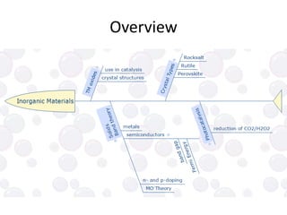
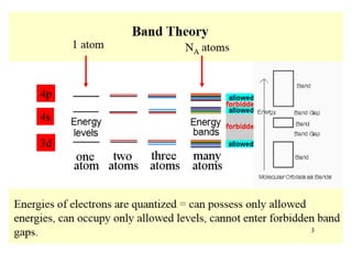
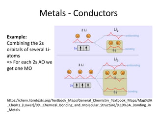
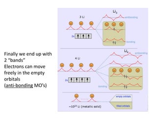
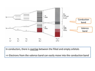
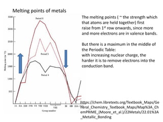
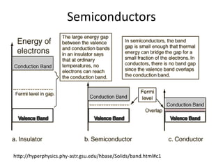
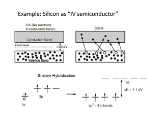
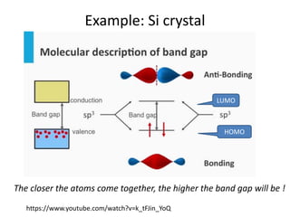
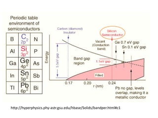
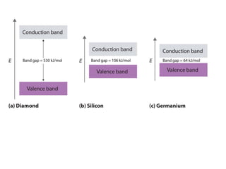
Inorganic Materials (1)
Electrical, Optical and Magnetic
Properties of solids
Dr.Chris, UP April 2018
Overview
Properties of
Transition Metal oxides
Dr. Christoph, UP April 2018
Important industrial processes
Crystal Structures
Octahedral
holes =
no of O2-
Tetrahedral holes
=
½ of octahedral
Spinel Types M2+ M3+
2 O4
Review: Crystal Structures
https://www.engr.uvic.ca/~mech466/MECH466-Lecture-3.pdf
Positions in a crystal
 = in the center
M = middle of a edge
R = at the edge
Band Theory
https://is.muni.cz/el/1431/podzim2017/C7780/um/L4_band_theory.pdf
Metals - Conductors
Example:
Combining the 2s
orbitals of several Li-
atoms
=> For each 2s AO we
get one MO
https://chem.libretexts.org/Textbook_Maps/General_Chemistry_Textbook_Maps/Map%3A
_Chem1_(Lower)/09._Chemical_Bonding_and_Molecular_Structure/9.10%3A_Bonding_in
_Metals
Finally we end up with
2 “bands”
Electrons can move
freely in the empty
orbitals
(anti-bonding MO’s)
In conductors, there is overlap between the filled and empty orbitals
=> Electrons from the valence band can easily move into the conduction band
Conduction
band
Valence
band
The melting points ( ~ the strength which
that atoms are held together) first
raise from 1st row onwards, since more
and more electrons are in valence bands.
But there is a maximum in the middle of
the Periodic Table:
with increasing nuclear charge, the
harder it is to remove electrons into the
conduction band.
https://chem.libretexts.org/Textbook_Maps/Ge
neral_Chemistry_Textbook_Maps/Map%3A_Ch
emPRIME_(Moore_et_al.)/22Metals/22.01%3A
_Metallic_Bonding
Melting points of metals
Semiconductors
http://hyperphysics.phy-astr.gsu.edu/hbase/Solids/band.html#c1
Example: Silicon as “IV semiconductor”
Example: Si crystal
The closer the atoms come together, the higher the band gap will be !
LUMO
HOMO
https://www.youtube.com/watch?v=k_tFJin_YoQ
http://hyperphysics.phy-astr.gsu.edu/hbase/Solids/bandper.html#c1
Questions
empty
electrons
Question 2
https://chem.libretexts.org/LibreTexts/University_of_Missouri/MU%3A__1330H_(Keller)/
12%3A_Solids_and_Modern_Materials/12.1%3A_Classes_of_Materials
The probability to find and electron
in the conductor band can be
calculated as:
https://chem.libretexts.org/Core/Physical_and_Theoretical_Chemistry/Chemical_Bonding/F
undamentals_of_Chemical_Bonding/Band_Structure
Influence of Temperature
Typical semiconductors
Elements:
• With 4 valence electrons: Si, Ge
• With 3 and 5 VE: GaAs, GaP, GaSb
III-V semiconductors
The smaller the lattice constant, the higher the band gap energy
II-VI semiconductors
https://www.azonano.com/article.aspx?ArticleID=4226
Measure the band gap energy by UV/VIS
Fermi Level EF (metals)
EF = 50% probability level to find an electron
https://www.youtube.com/watch?v=zWOSAzbxTrE
For semiconductors, EF is in the middle of the band gap
The higher T, the more electrons
will come up to the conductive
band –
at 0 K, all electrons are in the
valence band
T up
Charge
carriers are
electrons
and holes
Inorganic materials 1/2

Inorganic materials 1/2