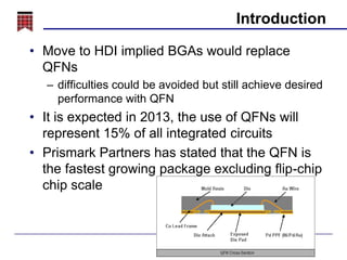
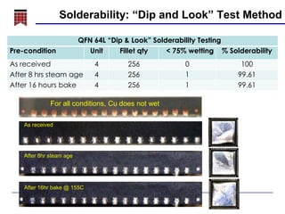
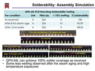
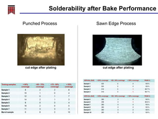
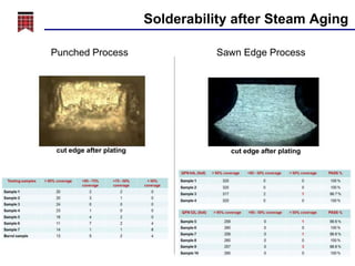
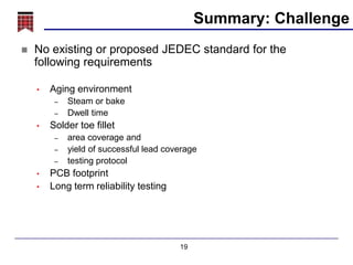
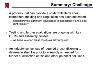
Improved QFN
Reliability Process
Dr. John Ganjei
©2014 ASQ & Presentation Ganjei

http://reliabilitycalendar.org/webina
rs/
ASQ Reliability Division
English Webinar Series
One of the monthly webinars
on topics of interest to
reliability engineers.
To view recorded webinar (available to ASQ Reliability
Division members only) visit asq.org/reliability
To sign up for the free and available to anyone live
webinars visit reliabilitycalendar.org and select English
Webinars to find links to register for upcoming events

http://reliabilitycalendar.org/webina
rs/
ASQ RD Webinar Series
Improved QFN Reliability Process
Thursday January 9, 2014 9-10am PST
Presented by: Dr. John Ganjei

3
Outline/Agenda
• Introduction
–Design and criteria

• Discussion Topics
–Industry requirements

• Performance Assessment
–Various solderability tests

• Summary
• Acknowledgements
–MacDermid Southeast Asia Team
Introduction
• Move to HDI implied BGAs would replace
QFNs
– difficulties could be avoided but still achieve desired
performance with QFN

• It is expected in 2013, the use of QFNs will
represent 15% of all integrated circuits
• Prismark Partners has stated that the QFN is
the fastest growing package excluding flip-chip
chip scale
Design
• A copper foil lead frame is pattern etched or
punched for the package assembly process.
• Singulation can be either punched or sawn.
– copper edges become exposed leaving terminations
susceptible to oxidation
– can degrade solderability during component assembly
to the mating circuit board.
Design
• The designer must consider:
– some devices may have oxidized and termination ends
will not ‘wet’ during assembly processing.
JH

JT

JH

G

Solder fillet on bare Cu terminal
end with oxidation build-up

JT
G

Solder fillet on coated or
plated terminal end

Reference:
IPC Webinar June 23, 2011
Industry Requirements
• Currently there are no industry (IPC or JEDEC)
requirements for toe fillet wetting
• OEMs are working toward stronger industry
wide specifications to ensure the performance
and reliability of this component style.
• An industry group should decide on the
appropriate preconditioning and fillet height
requirements
Toe Fillet Solderability
BOARD LEVEL ASSEMBLY AND RELIABILITY CONSIDERATIONS
FOR QFN TYPE PACKAGES
Ahmer Syed and WonJoon Kang
Amkor Technology, Inc.
Finite element simulations and actual test data generated by
customer have shown that the fillets - if formed - can
improve the board level reliability by as much as 2X for a
package with large die to package size ratio. The fillet extends
the length of solder joint and provides a longer path
for the crack to go through the entire joint, thus improving
the reliability.



Soldered fillet would deliver higher joint reliability
 More



soldered interface

Enable inspectability
Process Introduction
• Proposed chemical plating for producing a
solderable sidewall
– Can be applied vertically, horizontally or in barrel
machines

• Will clean the edges and make a more uniform
surface for plating.
• Flank plating can be performed on parts after
singulation
– either mounted on tape or in singulated form.

• No appearance or morphology change is observed
to the original electroplated tin
Performance Assessment
• Effect on part integrity and electrolytic tin
plating
• Laboratory solderability testing
– Dip and look

• Assembly simulation at HKUST
Performance Assessment
Cu oxides

Sawing burr

Before the process

After the process
Performance Assessment
Before the process

1000x

After the process

1000x

• After proposed process, no appearance or morphology
change is observed from the original tin plating of the
DAP and lead terminals by scope or visual
Solderability: “Dip and Look” Test Method

Tweezers

JESD22-B102E
•
•
•
•

Solder: Sn96.5 Ag3.0 Cu0.5
Solder temp: 245 C
Flux type:ROL0
Immersion time in flux: 5 -10sec.
– Flux drip time ~ 10 sec. before
dipping into the solder

• Immersion time at solder: 5 sec.
• Use tweezers to grasp two
corner of testing unit and dip the
whole unit at 90 into the solder
Solder pot
Solderability: “Dip and Look” Test Method
Pre-condition

QFN 64L “Dip & Look” Solderability Testing
Unit
Fillet qty
< 75% wetting % Solderability

As received
After 8 hrs steam age
After 16 hours bake

4
4
4

256
256
256

For all conditions, Cu does not wet
As received

After 8hr steam age

After 16hr bake @ 155C

0
1
1

100
99.61
99.61
Solderability: Assembly Simulation
QFN 64L PCB Mounting Solderability Testing
Pre-condition

Unit

Fillet qty

< 75% wetting

% Solderability

As received

4

256

0

100

After 8 hrs steam age

4

256

10

96.09

After 16 hrs bake

4

256

5

98.05

For all conditions, Cu does not wet
As received

After 8 hr steam age

After 16 hr bake 155oC

Non wetting

Less wetting

• QFN 64L can achieve 100% solder coverage as received
• Some less wetting observed after the steam aging and high
temperature exposures
Solderability after Bake Performance
Punched Process

cut edge after plating

Sawn Edge Process

cut edge after plating
Solderability after Steam Aging
Punched Process

cut edge after plating

Sawn Edge Process

cut edge after plating
Summary: Challenge


No existing or proposed JEDEC standard for the
following requirements
•

Aging environment
–
–

•

Solder toe fillet
–
–
–

•
•

Steam or bake
Dwell time
area coverage and
yield of successful lead coverage
testing protocol

PCB footprint
Long term reliability testing

19
Summary: Challenge
• A process that can provide a solderable flank after
component molding and singulation has been described
– should provide significant advantages in inspectability and solder
joint reliability.

• Testing and further evaluations are ongoing with key
OEMs and assembly houses
– we hope to report these results as they progress.

• An industry consensus of required preconditioning to
determine shelf life prior to assembly is needed for
further qualification of this and other potential solutions.
Acknowledgements
• I’d like to thank my coauthors
– Mr. Rich Retallick
– Ms Lenora Toscano
– Especially Dr. Gu Hong for his research and
development efforts which made this paper possible

– Also the team at HKUST

Thank You!

ASQ RD Webinar: Improved QFN Reliability Process

  • 1.
    Improved QFN Reliability Process Dr.John Ganjei ©2014 ASQ & Presentation Ganjei http://reliabilitycalendar.org/webina rs/
  • 2.
    ASQ Reliability Division EnglishWebinar Series One of the monthly webinars on topics of interest to reliability engineers. To view recorded webinar (available to ASQ Reliability Division members only) visit asq.org/reliability To sign up for the free and available to anyone live webinars visit reliabilitycalendar.org and select English Webinars to find links to register for upcoming events http://reliabilitycalendar.org/webina rs/
  • 3.
    ASQ RD WebinarSeries Improved QFN Reliability Process Thursday January 9, 2014 9-10am PST Presented by: Dr. John Ganjei 3
  • 4.
    Outline/Agenda • Introduction –Design andcriteria • Discussion Topics –Industry requirements • Performance Assessment –Various solderability tests • Summary • Acknowledgements –MacDermid Southeast Asia Team
  • 5.
    Introduction • Move toHDI implied BGAs would replace QFNs – difficulties could be avoided but still achieve desired performance with QFN • It is expected in 2013, the use of QFNs will represent 15% of all integrated circuits • Prismark Partners has stated that the QFN is the fastest growing package excluding flip-chip chip scale
  • 6.
    Design • A copperfoil lead frame is pattern etched or punched for the package assembly process. • Singulation can be either punched or sawn. – copper edges become exposed leaving terminations susceptible to oxidation – can degrade solderability during component assembly to the mating circuit board.
  • 7.
    Design • The designermust consider: – some devices may have oxidized and termination ends will not ‘wet’ during assembly processing. JH JT JH G Solder fillet on bare Cu terminal end with oxidation build-up JT G Solder fillet on coated or plated terminal end Reference: IPC Webinar June 23, 2011
  • 8.
    Industry Requirements • Currentlythere are no industry (IPC or JEDEC) requirements for toe fillet wetting • OEMs are working toward stronger industry wide specifications to ensure the performance and reliability of this component style. • An industry group should decide on the appropriate preconditioning and fillet height requirements
  • 9.
    Toe Fillet Solderability BOARDLEVEL ASSEMBLY AND RELIABILITY CONSIDERATIONS FOR QFN TYPE PACKAGES Ahmer Syed and WonJoon Kang Amkor Technology, Inc. Finite element simulations and actual test data generated by customer have shown that the fillets - if formed - can improve the board level reliability by as much as 2X for a package with large die to package size ratio. The fillet extends the length of solder joint and provides a longer path for the crack to go through the entire joint, thus improving the reliability.  Soldered fillet would deliver higher joint reliability  More  soldered interface Enable inspectability
  • 10.
    Process Introduction • Proposedchemical plating for producing a solderable sidewall – Can be applied vertically, horizontally or in barrel machines • Will clean the edges and make a more uniform surface for plating. • Flank plating can be performed on parts after singulation – either mounted on tape or in singulated form. • No appearance or morphology change is observed to the original electroplated tin
  • 11.
    Performance Assessment • Effecton part integrity and electrolytic tin plating • Laboratory solderability testing – Dip and look • Assembly simulation at HKUST
  • 12.
    Performance Assessment Cu oxides Sawingburr Before the process After the process
  • 13.
    Performance Assessment Before theprocess 1000x After the process 1000x • After proposed process, no appearance or morphology change is observed from the original tin plating of the DAP and lead terminals by scope or visual
  • 14.
    Solderability: “Dip andLook” Test Method Tweezers JESD22-B102E • • • • Solder: Sn96.5 Ag3.0 Cu0.5 Solder temp: 245 C Flux type:ROL0 Immersion time in flux: 5 -10sec. – Flux drip time ~ 10 sec. before dipping into the solder • Immersion time at solder: 5 sec. • Use tweezers to grasp two corner of testing unit and dip the whole unit at 90 into the solder Solder pot
  • 15.
    Solderability: “Dip andLook” Test Method Pre-condition QFN 64L “Dip & Look” Solderability Testing Unit Fillet qty < 75% wetting % Solderability As received After 8 hrs steam age After 16 hours bake 4 4 4 256 256 256 For all conditions, Cu does not wet As received After 8hr steam age After 16hr bake @ 155C 0 1 1 100 99.61 99.61
  • 16.
    Solderability: Assembly Simulation QFN64L PCB Mounting Solderability Testing Pre-condition Unit Fillet qty < 75% wetting % Solderability As received 4 256 0 100 After 8 hrs steam age 4 256 10 96.09 After 16 hrs bake 4 256 5 98.05 For all conditions, Cu does not wet As received After 8 hr steam age After 16 hr bake 155oC Non wetting Less wetting • QFN 64L can achieve 100% solder coverage as received • Some less wetting observed after the steam aging and high temperature exposures
  • 17.
    Solderability after BakePerformance Punched Process cut edge after plating Sawn Edge Process cut edge after plating
  • 18.
    Solderability after SteamAging Punched Process cut edge after plating Sawn Edge Process cut edge after plating
  • 19.
    Summary: Challenge  No existingor proposed JEDEC standard for the following requirements • Aging environment – – • Solder toe fillet – – – • • Steam or bake Dwell time area coverage and yield of successful lead coverage testing protocol PCB footprint Long term reliability testing 19
  • 20.
    Summary: Challenge • Aprocess that can provide a solderable flank after component molding and singulation has been described – should provide significant advantages in inspectability and solder joint reliability. • Testing and further evaluations are ongoing with key OEMs and assembly houses – we hope to report these results as they progress. • An industry consensus of required preconditioning to determine shelf life prior to assembly is needed for further qualification of this and other potential solutions.
  • 21.
    Acknowledgements • I’d liketo thank my coauthors – Mr. Rich Retallick – Ms Lenora Toscano – Especially Dr. Gu Hong for his research and development efforts which made this paper possible – Also the team at HKUST Thank You!