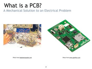
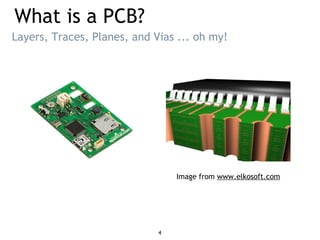
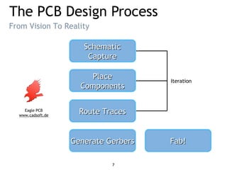
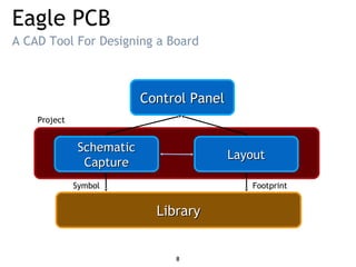
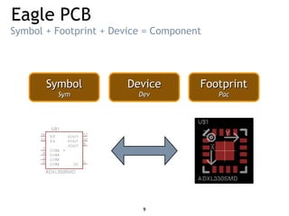
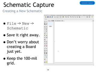
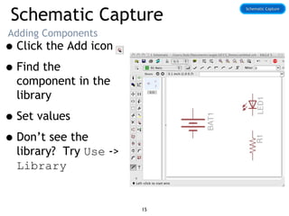
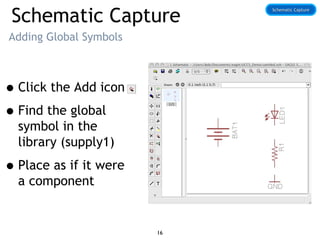
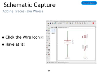
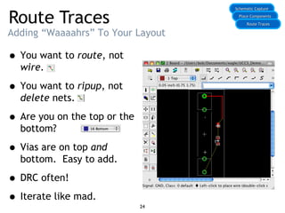
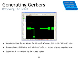
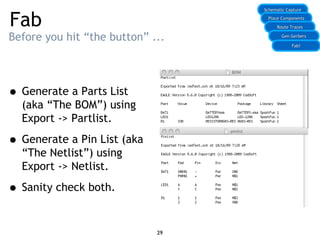
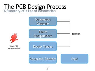
How to Design
Printed Circuits
Boards
... and live to tell about it.
Bob Kressin, Instructor
Department of Electrical Engineering and Computer Science
Overview
•What is a Printed Circuit Board?
•How do you design a PCB?
•How do you order a custom PCB?
2
What is a PCB?
A Mechanical Solution to an Electrical Problem
Photo from www.sparkfun.com
3
Photo from hephaestusaudio.com
What is a PCB?
Layers, Traces, Planes, and Vias ... oh my!
Image from www.elkosoft.com
4
What is a PCB?
Image from www.gettyimages.com
Essentially, you’re job is this ...
5
Component Suppliers
•For the “weird & wonderful” -
•For the “inexpensive everyday” -
•For the board itself -
Where do we get the goods?
www.sparkfun.com
www.mouser.com
www.4pcb.com
The PCB Design Process
From Vision To Reality
Eagle PCB
www.cadsoft.de
7
PlacePlace
ComponentsComponents
Route TracesRoute Traces
Fab!Fab!
Iteration
Generate GerbersGenerate Gerbers
SchematicSchematic
CaptureCapture
Eagle PCB
A CAD Tool For Designing a Board
SchematicSchematic
CaptureCapture
LayoutLayout
Control PanelControl Panel
LibraryLibrary
Symbol Footprint
Project
8
Eagle PCB
Symbol + Footprint + Device = Component
DeviceDevice
DevDev
SymbolSymbol
SymSym
FootprintFootprint
PacPac
9
Eagle PCB
•A Plan
•Block Diagram / Napkin Sketch
•Component Selection
•Connections and Testing Considerations
•Power and Performance Considerations
•A New Project
•Access to Libraries
Stuff I Need To Get Started
10
Eagle PCB
It’s all about the planning.
ComponentsComponents ConnectionsConnections
Power &Power &
PerformancePerformance
Passives: 0805,
0603, etc.
IC Packages:
QFN, TQFP, etc.
Libraries
Mechanical
Connections
Bus Connections
PC Connections
Power Ratings
Battery
Performance
High-Speed /
High-Sensitivity
11
Eagle PCB
Creating a New Project
•Launch Eagle
•File -> New -> Project
•Enter Project Name
•Directory structure taken care of automagically.
•Active project is shown with a green light.
12
Eagle PCB
Accessing Libraries
•Full view of libraries available via Control Panel
•Download more from the web and place in the
Eagle installation directory in /lbr
•Sparkfun has an incredible library of more
advanced parts (accelerometers, etc.)
•Caution! Just because you see the library in
Control Panel doesn’t mean you can access it in
your schematic.
13
Schematic Capture
Creating a New Schematic
•File -> New ->
Schematic
•Save it right away.
•Don’t worry about
creating a Board
just yet.
•Keep the 100-mil
grid.
Schematic CaptureSchematic Capture
14
Schematic Capture
Adding Components
•Click the Add icon
•Find the
component in the
library
•Set values
•Don’t see the
library? Try Use ->
Library
Schematic CaptureSchematic Capture
15
Schematic Capture
Adding Global Symbols
•Click the Add icon
•Find the global
symbol in the
library (supply1)
•Place as if it were
a component
Schematic CaptureSchematic Capture
16
Schematic Capture
Adding Traces (aka Wires)
•Click the Wire icon
•Have at it!
Schematic CaptureSchematic Capture
17
Schematic Capture
Some General Tips
• Avoid changing the grid unless absolutely necessary.
• Free Eagle version does not allow “sheets”.
• Free Eagle version requires that schematic drives the
layout ... not vice-versa.
• Groups, Info, and Layers icons are useful.
• Pan, zoom, niceties easy to use.
• Really care about that “net”? Label it.
• Keep it clean - don’t be lazy.
• Document!
Schematic CaptureSchematic Capture
18
Place Components
But before you do ...
• Passives - 0805 means 0.08” by 0.05”
• Connectors - beware of physical fit
• Actives - lots of packaging alternatives
• Give thought to testability and troubleshooting
Schematic CaptureSchematic Capture
DIP LQFP, QFP, TQFP QFN BGA
Thru-Hole (TH)Thru-Hole (TH) Surface Mount (SMT)Surface Mount (SMT)
Place ComponentsPlace Components
19
Place Components
Creating a new board design
• From the schematic,
choose File ->
Switch to Board.
• “Create From
Schematic”? You bet!
• Board window
automatically opens.
Schematic CaptureSchematic Capture
Place ComponentsPlace Components
20
Place Components
Some Common Tasks
• Right-click on top of
component, select
Move to reposition.
• While moving, right-
click to Rotate.
• Use “Group” wisely.
• Right-click to Mirror
(change to other side
of board)
• Use Move to change
outline
Schematic CaptureSchematic Capture
Place ComponentsPlace Components
21
Place Components
Thinking ahead
• Take your time.
• Untangle flight lines.
• Think about planes.
• Consider testability.
• Mechanical Fit?
• Hard stuff first.
• Keep silkscreen.
• Think hard about components
on 2-sides.
Schematic CaptureSchematic Capture
Place ComponentsPlace Components
22
Place Components
Some General Tips
• Are your Design Rules setup correctly?
• Run the Design Rule Check (DRC) often.
• Run the Electrical Rule Check (ERC) often.
• Save a snapshot of your placement file.
Schematic CaptureSchematic Capture
Place ComponentsPlace Components
23
Route Traces
Adding “Waaaahrs” To Your Layout
• You want to route, not
wire.
• You want to ripup, not
delete nets.
• Are you on the top or the
bottom?
• Vias are on top and
bottom. Easy to add.
• DRC often!
• Iterate like mad.
Schematic CaptureSchematic Capture
Place ComponentsPlace Components
Route TracesRoute Traces
24
Route Traces
Some General Tips
• Two layers? Have an x-
layer and a y-layer.
• Don’t forget mounting
holes, other nice things.
• Add testability features.
• Do the “what if?” dance.
• Do the cardboard
mockup.
• Pour Copper.
Schematic CaptureSchematic Capture
Place ComponentsPlace Components
Route TracesRoute Traces
25
Generating Gerbers
Some General Tips
• Using Advanced Circuits? Have I got a script for you ...
• This involves the “CAM Processor” ...
• Generate critical layers.
Schematic CaptureSchematic Capture
Place ComponentsPlace Components
Route TracesRoute Traces
26
Gen GerbersGen Gerbers
Easier
than spit!
Generating Gerbers
Sanity Checking The Result
• You’ll need an account with Advanced Circuits.
• Email will be sent confirming design rule checking.
• Advanced Circuits even gives you a discount.
• Squash any errors, review all warnings. Look for open vias, closed vias, etc.
Schematic CaptureSchematic Capture
Place ComponentsPlace Components
Route TracesRoute Traces
27
Gen GerbersGen Gerbers
freedfm.com
Generating Gerbers
Reviewing The Result
• ViewMate - Free Gerber Viewer for Microsoft Windows (link on Dr. Wickert’s site).
• Review planes, drill holes, and “obvious” defects. Not usually any surprises here.
• Biggest error - not exporting the proper layers.
Schematic CaptureSchematic Capture
Place ComponentsPlace Components
Route TracesRoute Traces
28
Gen GerbersGen Gerbers
Fab
Before you hit “the button” ...
Schematic CaptureSchematic Capture
Place ComponentsPlace Components
Route TracesRoute Traces
29
• Generate a Parts List
(aka “The BOM”) using
Export -> Partlist.
• Generate a Pin List (aka
“The Netlist”) using
Export -> Netlist.
• Sanity check both.
Gen GerbersGen Gerbers
Fab!Fab!
Fab
Some General Tips
• Do you have all of your components? Lead time?
• Find out what file format your PCB Vendor wants.
• Advanced Circuits - GERBER_RS_274X (no, really)
• Consider routing it yourself at UCCS.
• Consider barebonespcb.com. Really cheap.
• Sleep on it. Follow my tradition -
30
Schematic CaptureSchematic Capture
Place ComponentsPlace Components
Route TracesRoute Traces
Gen GerbersGen Gerbers
Fab!Fab!
The PCB Design Process
A Summary of a Lot of Information
31
PlacePlace
ComponentsComponents
Route TracesRoute Traces
Fab!Fab!
Iteration
Eagle PCB
www.cadsoft.de
Generate GerbersGenerate Gerbers
SchematicSchematic
CaptureCapture

Pcb design process

  • 1.
    How to Design PrintedCircuits Boards ... and live to tell about it. Bob Kressin, Instructor Department of Electrical Engineering and Computer Science
  • 2.
    Overview •What is aPrinted Circuit Board? •How do you design a PCB? •How do you order a custom PCB? 2
  • 3.
    What is aPCB? A Mechanical Solution to an Electrical Problem Photo from www.sparkfun.com 3 Photo from hephaestusaudio.com
  • 4.
    What is aPCB? Layers, Traces, Planes, and Vias ... oh my! Image from www.elkosoft.com 4
  • 5.
    What is aPCB? Image from www.gettyimages.com Essentially, you’re job is this ... 5
  • 6.
    Component Suppliers •For the“weird & wonderful” - •For the “inexpensive everyday” - •For the board itself - Where do we get the goods? www.sparkfun.com www.mouser.com www.4pcb.com
  • 7.
    The PCB DesignProcess From Vision To Reality Eagle PCB www.cadsoft.de 7 PlacePlace ComponentsComponents Route TracesRoute Traces Fab!Fab! Iteration Generate GerbersGenerate Gerbers SchematicSchematic CaptureCapture
  • 8.
    Eagle PCB A CADTool For Designing a Board SchematicSchematic CaptureCapture LayoutLayout Control PanelControl Panel LibraryLibrary Symbol Footprint Project 8
  • 9.
    Eagle PCB Symbol +Footprint + Device = Component DeviceDevice DevDev SymbolSymbol SymSym FootprintFootprint PacPac 9
  • 10.
    Eagle PCB •A Plan •BlockDiagram / Napkin Sketch •Component Selection •Connections and Testing Considerations •Power and Performance Considerations •A New Project •Access to Libraries Stuff I Need To Get Started 10
  • 11.
    Eagle PCB It’s allabout the planning. ComponentsComponents ConnectionsConnections Power &Power & PerformancePerformance Passives: 0805, 0603, etc. IC Packages: QFN, TQFP, etc. Libraries Mechanical Connections Bus Connections PC Connections Power Ratings Battery Performance High-Speed / High-Sensitivity 11
  • 12.
    Eagle PCB Creating aNew Project •Launch Eagle •File -> New -> Project •Enter Project Name •Directory structure taken care of automagically. •Active project is shown with a green light. 12
  • 13.
    Eagle PCB Accessing Libraries •Fullview of libraries available via Control Panel •Download more from the web and place in the Eagle installation directory in /lbr •Sparkfun has an incredible library of more advanced parts (accelerometers, etc.) •Caution! Just because you see the library in Control Panel doesn’t mean you can access it in your schematic. 13
  • 14.
    Schematic Capture Creating aNew Schematic •File -> New -> Schematic •Save it right away. •Don’t worry about creating a Board just yet. •Keep the 100-mil grid. Schematic CaptureSchematic Capture 14
  • 15.
    Schematic Capture Adding Components •Clickthe Add icon •Find the component in the library •Set values •Don’t see the library? Try Use -> Library Schematic CaptureSchematic Capture 15
  • 16.
    Schematic Capture Adding GlobalSymbols •Click the Add icon •Find the global symbol in the library (supply1) •Place as if it were a component Schematic CaptureSchematic Capture 16
  • 17.
    Schematic Capture Adding Traces(aka Wires) •Click the Wire icon •Have at it! Schematic CaptureSchematic Capture 17
  • 18.
    Schematic Capture Some GeneralTips • Avoid changing the grid unless absolutely necessary. • Free Eagle version does not allow “sheets”. • Free Eagle version requires that schematic drives the layout ... not vice-versa. • Groups, Info, and Layers icons are useful. • Pan, zoom, niceties easy to use. • Really care about that “net”? Label it. • Keep it clean - don’t be lazy. • Document! Schematic CaptureSchematic Capture 18
  • 19.
    Place Components But beforeyou do ... • Passives - 0805 means 0.08” by 0.05” • Connectors - beware of physical fit • Actives - lots of packaging alternatives • Give thought to testability and troubleshooting Schematic CaptureSchematic Capture DIP LQFP, QFP, TQFP QFN BGA Thru-Hole (TH)Thru-Hole (TH) Surface Mount (SMT)Surface Mount (SMT) Place ComponentsPlace Components 19
  • 20.
    Place Components Creating anew board design • From the schematic, choose File -> Switch to Board. • “Create From Schematic”? You bet! • Board window automatically opens. Schematic CaptureSchematic Capture Place ComponentsPlace Components 20
  • 21.
    Place Components Some CommonTasks • Right-click on top of component, select Move to reposition. • While moving, right- click to Rotate. • Use “Group” wisely. • Right-click to Mirror (change to other side of board) • Use Move to change outline Schematic CaptureSchematic Capture Place ComponentsPlace Components 21
  • 22.
    Place Components Thinking ahead •Take your time. • Untangle flight lines. • Think about planes. • Consider testability. • Mechanical Fit? • Hard stuff first. • Keep silkscreen. • Think hard about components on 2-sides. Schematic CaptureSchematic Capture Place ComponentsPlace Components 22
  • 23.
    Place Components Some GeneralTips • Are your Design Rules setup correctly? • Run the Design Rule Check (DRC) often. • Run the Electrical Rule Check (ERC) often. • Save a snapshot of your placement file. Schematic CaptureSchematic Capture Place ComponentsPlace Components 23
  • 24.
    Route Traces Adding “Waaaahrs”To Your Layout • You want to route, not wire. • You want to ripup, not delete nets. • Are you on the top or the bottom? • Vias are on top and bottom. Easy to add. • DRC often! • Iterate like mad. Schematic CaptureSchematic Capture Place ComponentsPlace Components Route TracesRoute Traces 24
  • 25.
    Route Traces Some GeneralTips • Two layers? Have an x- layer and a y-layer. • Don’t forget mounting holes, other nice things. • Add testability features. • Do the “what if?” dance. • Do the cardboard mockup. • Pour Copper. Schematic CaptureSchematic Capture Place ComponentsPlace Components Route TracesRoute Traces 25
  • 26.
    Generating Gerbers Some GeneralTips • Using Advanced Circuits? Have I got a script for you ... • This involves the “CAM Processor” ... • Generate critical layers. Schematic CaptureSchematic Capture Place ComponentsPlace Components Route TracesRoute Traces 26 Gen GerbersGen Gerbers Easier than spit!
  • 27.
    Generating Gerbers Sanity CheckingThe Result • You’ll need an account with Advanced Circuits. • Email will be sent confirming design rule checking. • Advanced Circuits even gives you a discount. • Squash any errors, review all warnings. Look for open vias, closed vias, etc. Schematic CaptureSchematic Capture Place ComponentsPlace Components Route TracesRoute Traces 27 Gen GerbersGen Gerbers freedfm.com
  • 28.
    Generating Gerbers Reviewing TheResult • ViewMate - Free Gerber Viewer for Microsoft Windows (link on Dr. Wickert’s site). • Review planes, drill holes, and “obvious” defects. Not usually any surprises here. • Biggest error - not exporting the proper layers. Schematic CaptureSchematic Capture Place ComponentsPlace Components Route TracesRoute Traces 28 Gen GerbersGen Gerbers
  • 29.
    Fab Before you hit“the button” ... Schematic CaptureSchematic Capture Place ComponentsPlace Components Route TracesRoute Traces 29 • Generate a Parts List (aka “The BOM”) using Export -> Partlist. • Generate a Pin List (aka “The Netlist”) using Export -> Netlist. • Sanity check both. Gen GerbersGen Gerbers Fab!Fab!
  • 30.
    Fab Some General Tips •Do you have all of your components? Lead time? • Find out what file format your PCB Vendor wants. • Advanced Circuits - GERBER_RS_274X (no, really) • Consider routing it yourself at UCCS. • Consider barebonespcb.com. Really cheap. • Sleep on it. Follow my tradition - 30 Schematic CaptureSchematic Capture Place ComponentsPlace Components Route TracesRoute Traces Gen GerbersGen Gerbers Fab!Fab!
  • 31.
    The PCB DesignProcess A Summary of a Lot of Information 31 PlacePlace ComponentsComponents Route TracesRoute Traces Fab!Fab! Iteration Eagle PCB www.cadsoft.de Generate GerbersGenerate Gerbers SchematicSchematic CaptureCapture