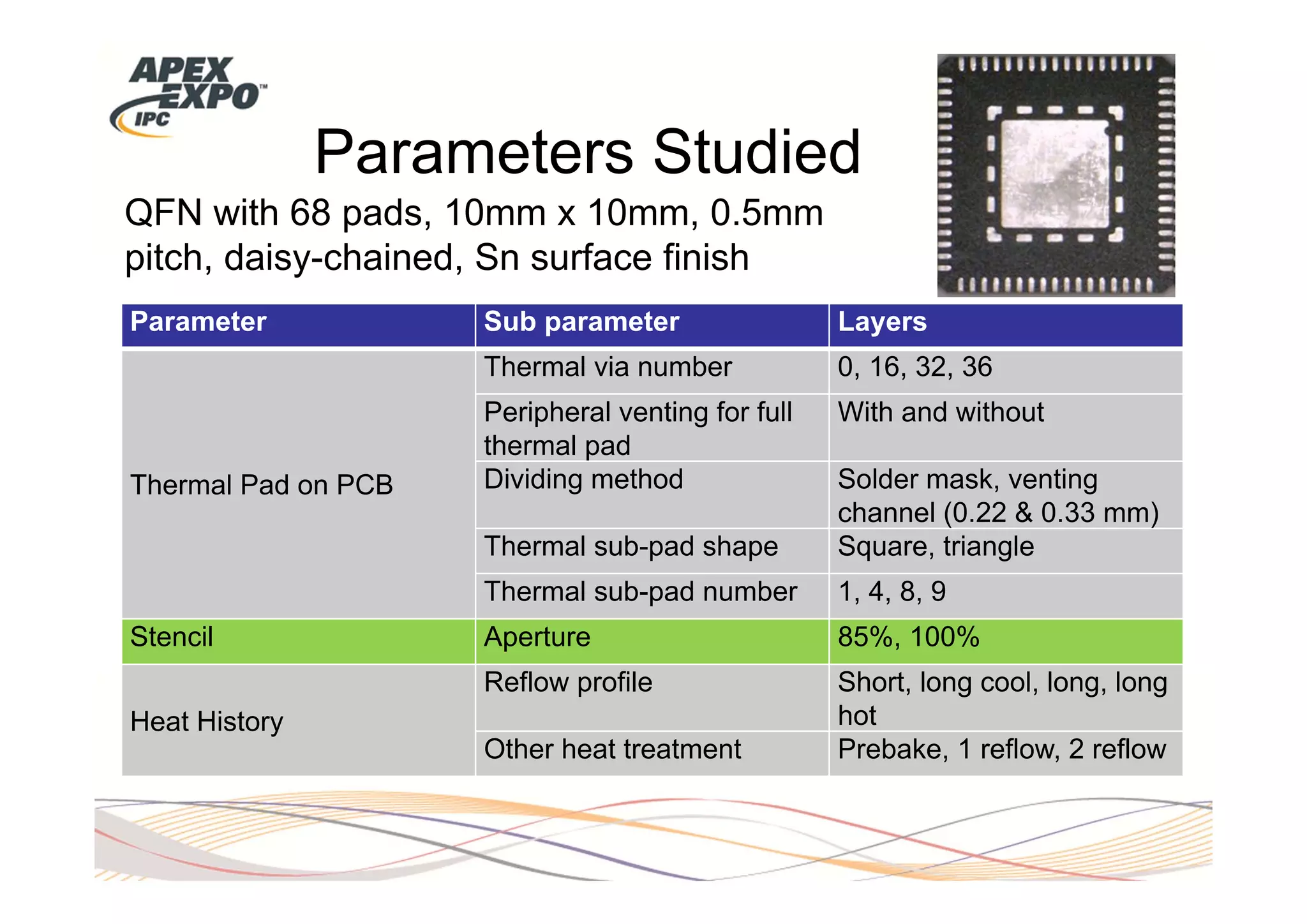
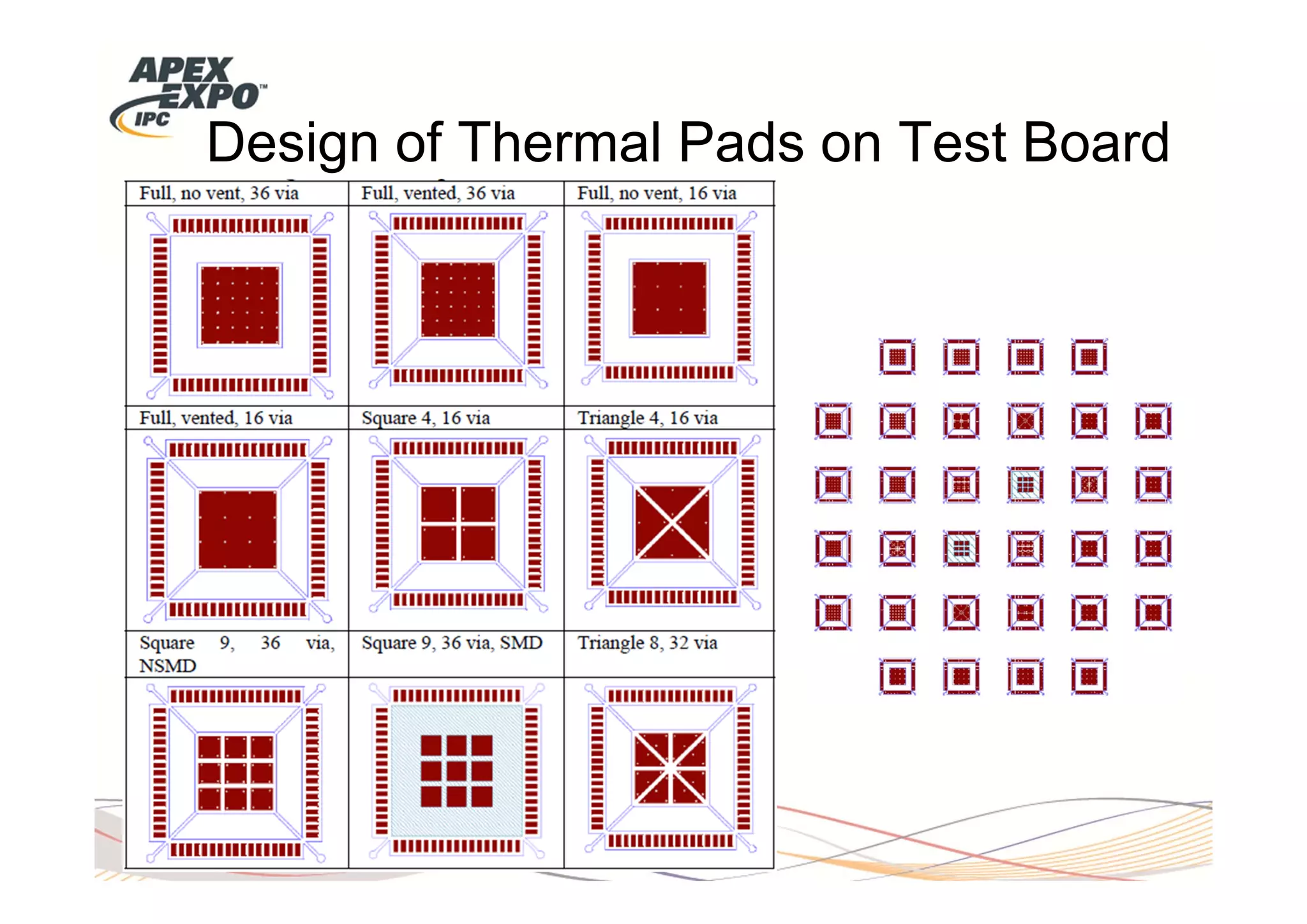
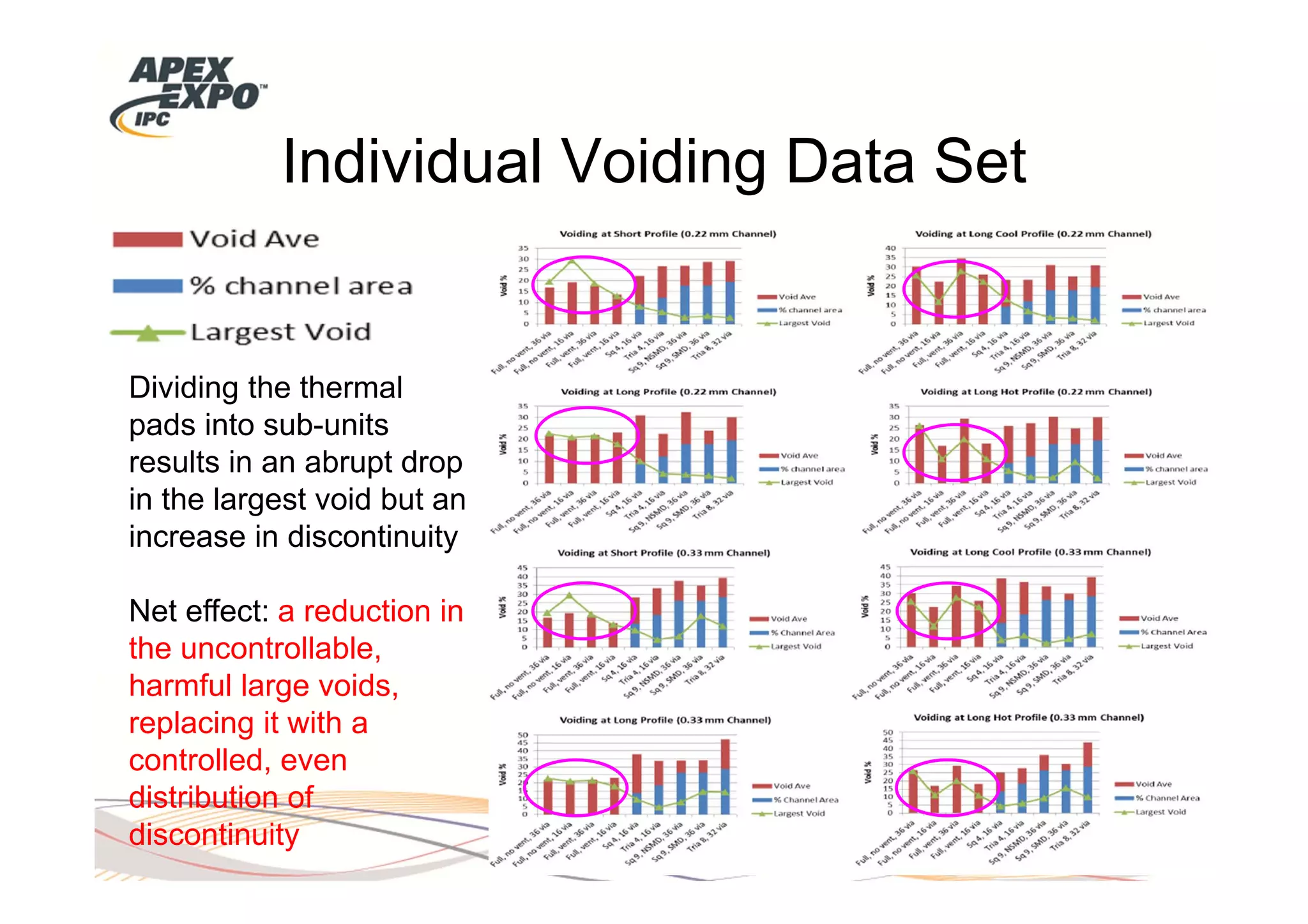
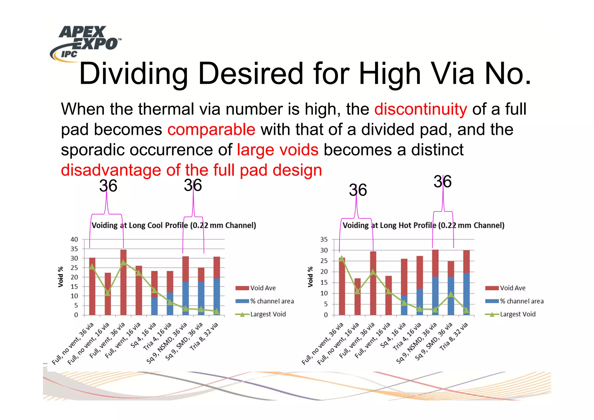
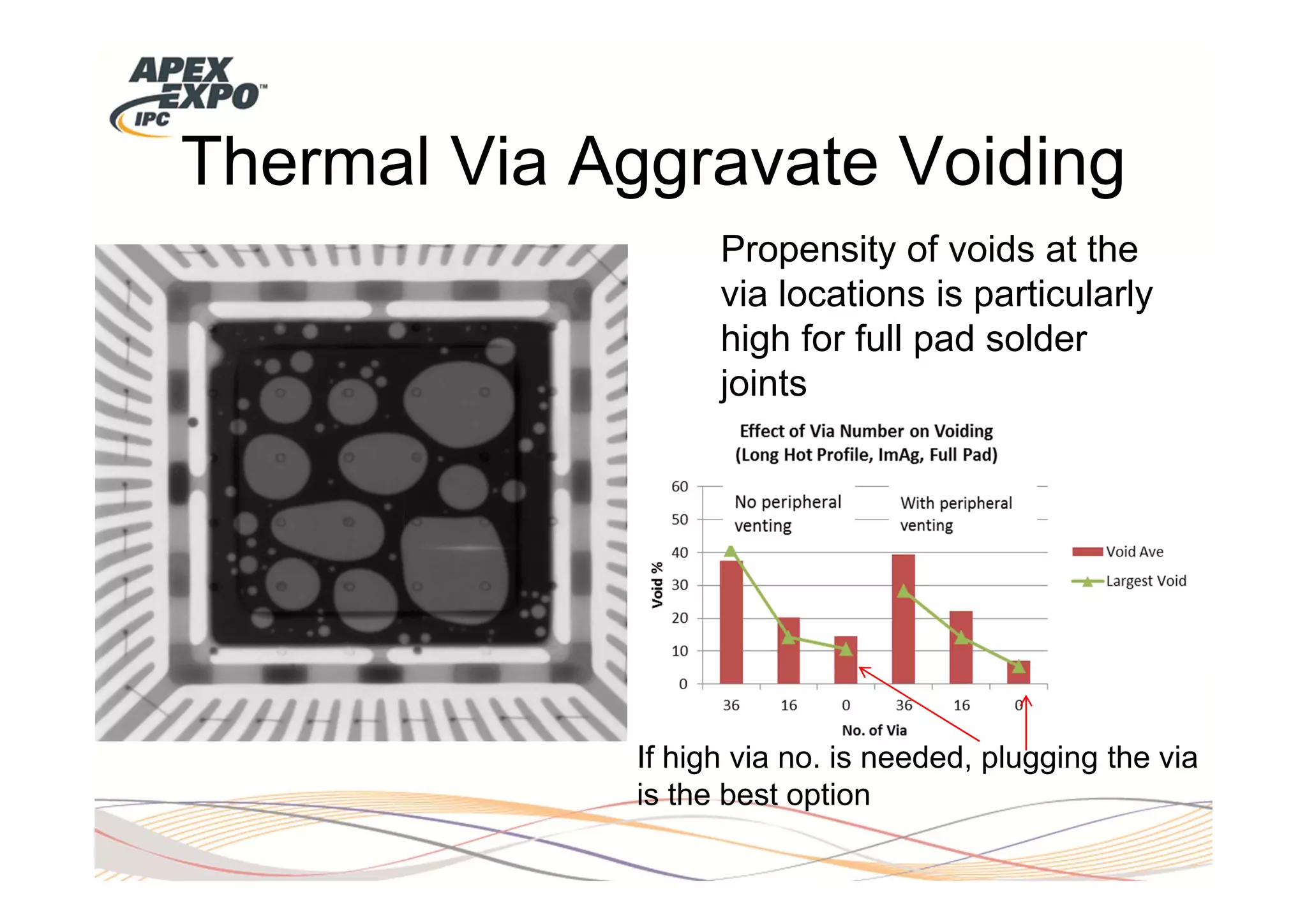
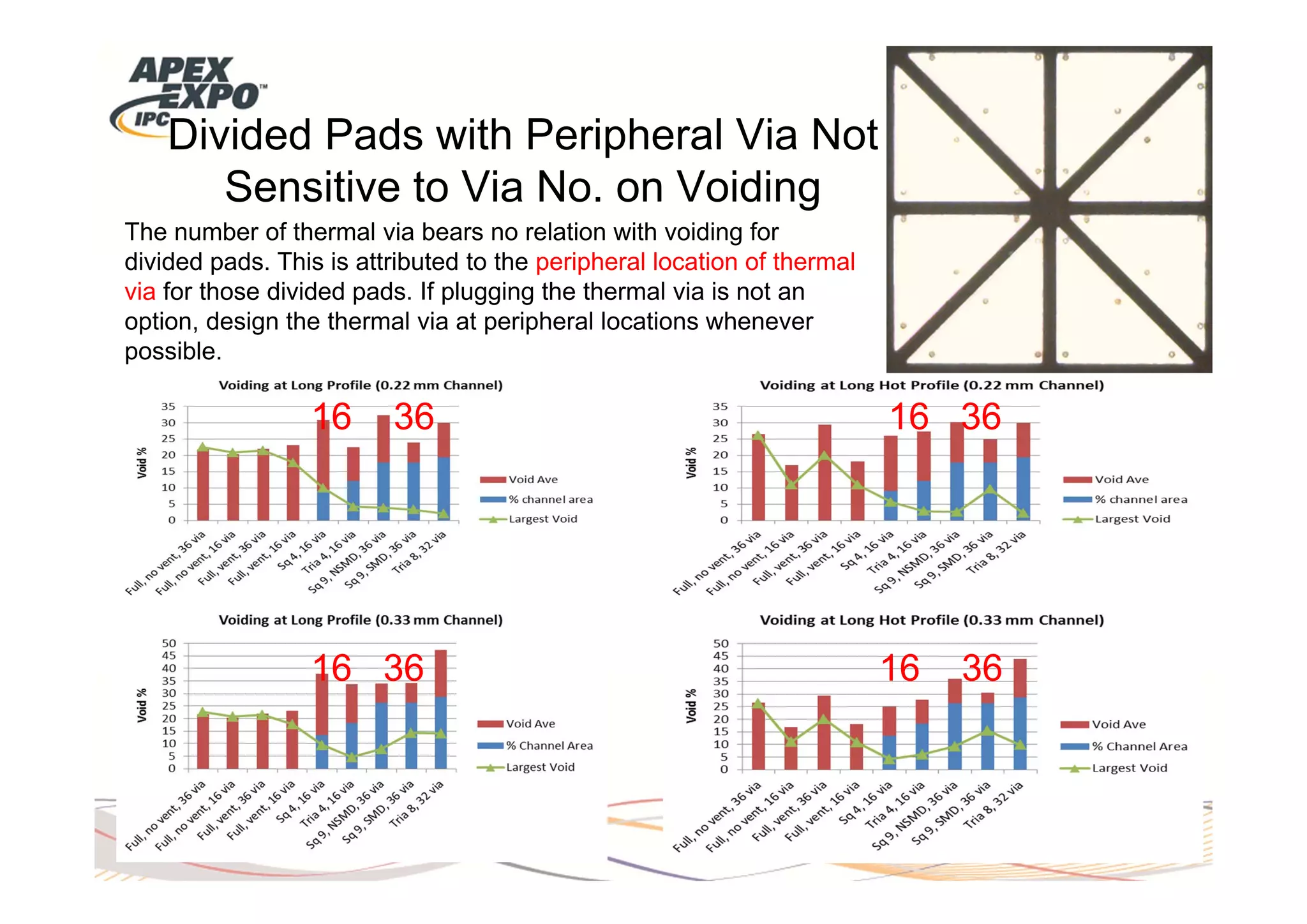
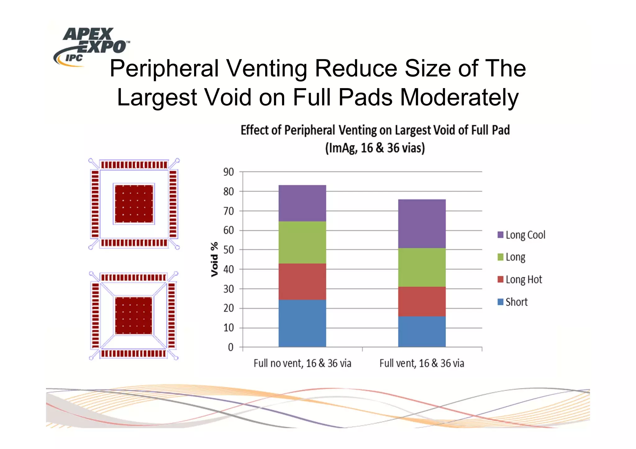
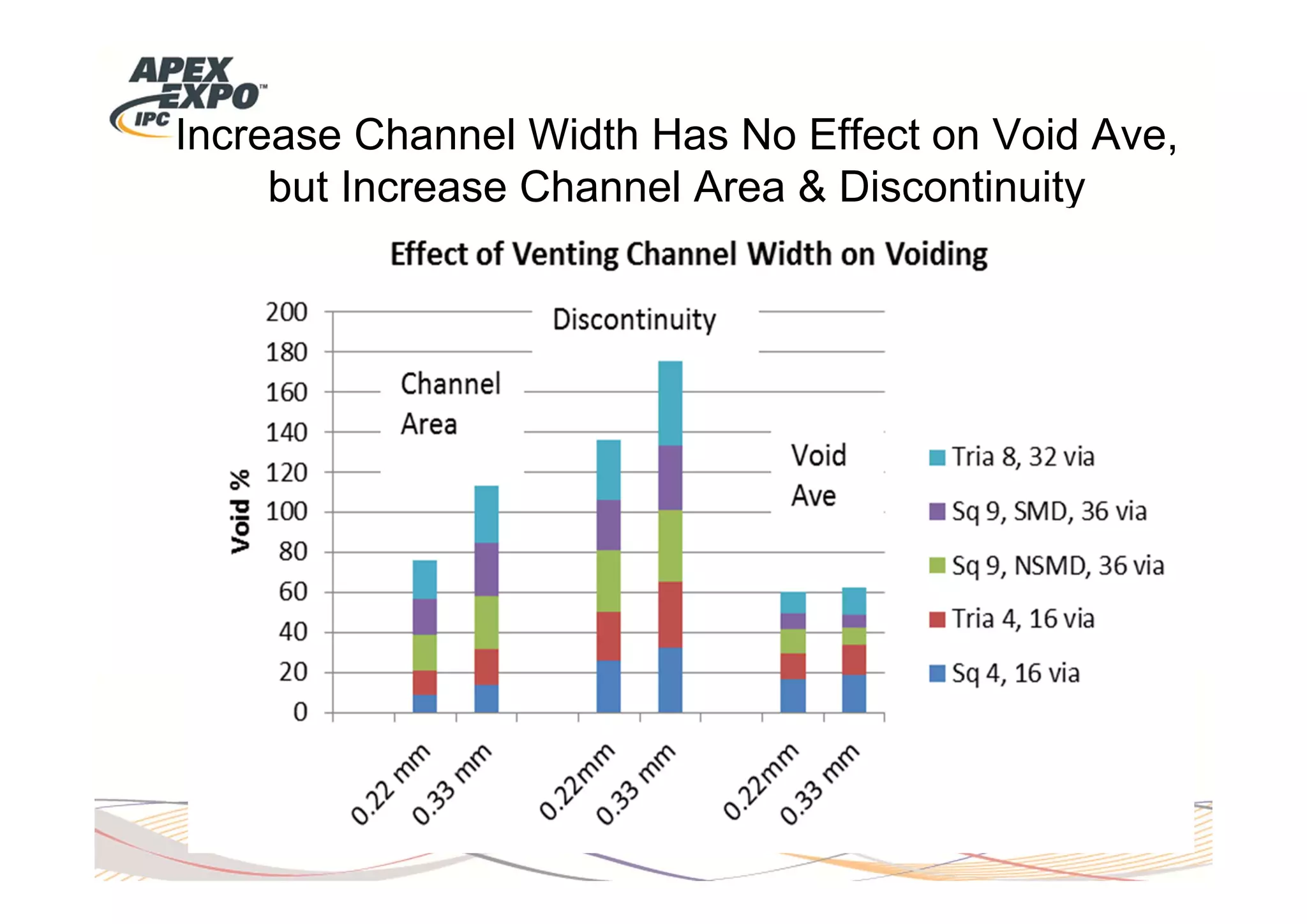
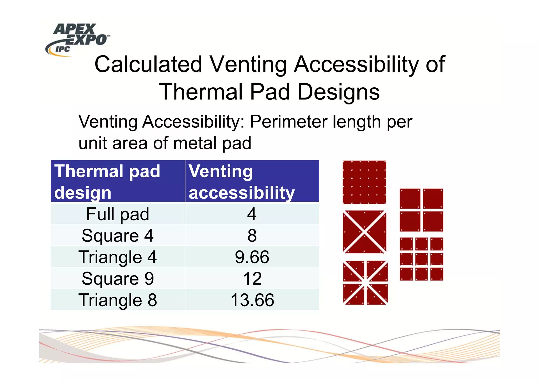
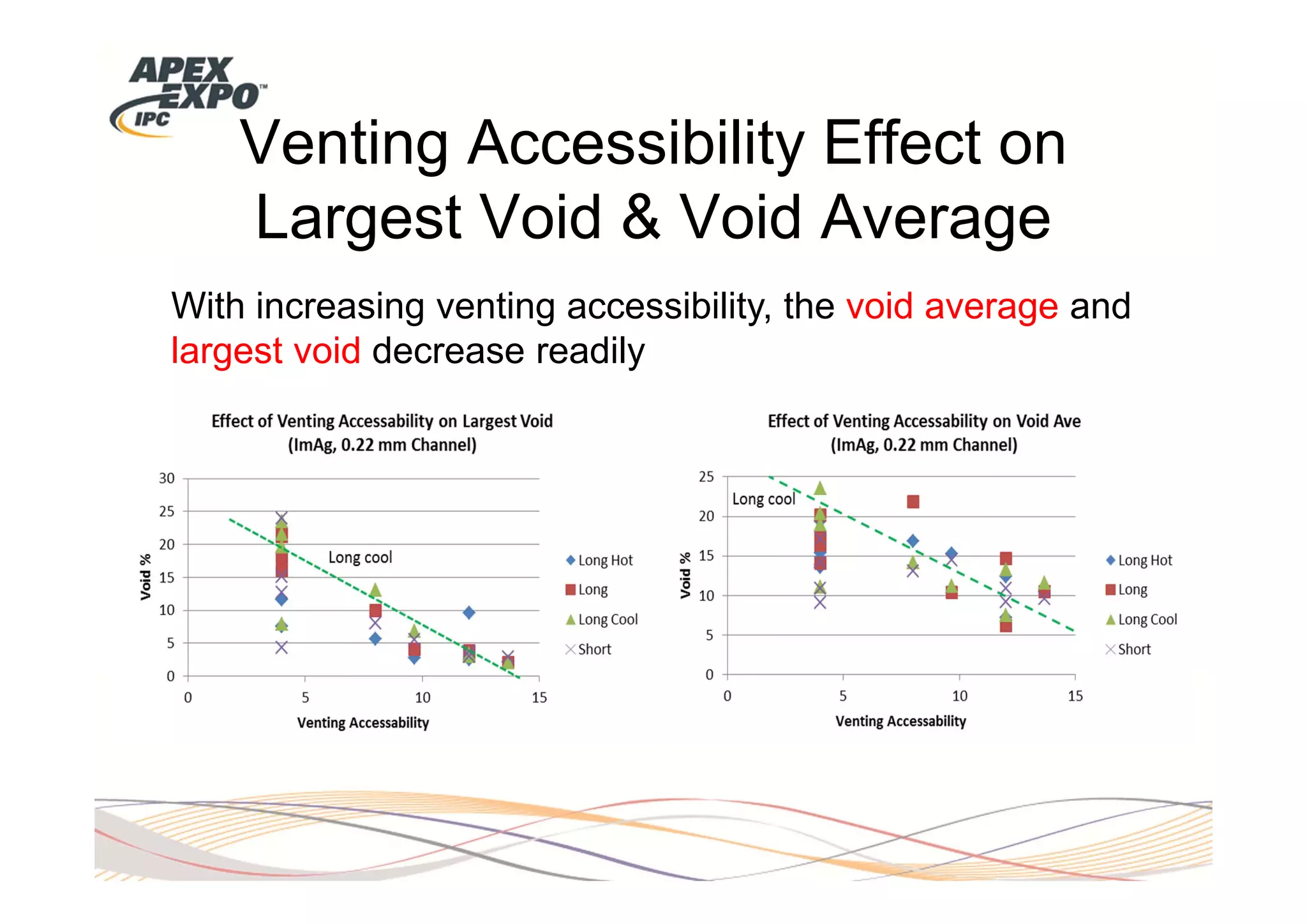
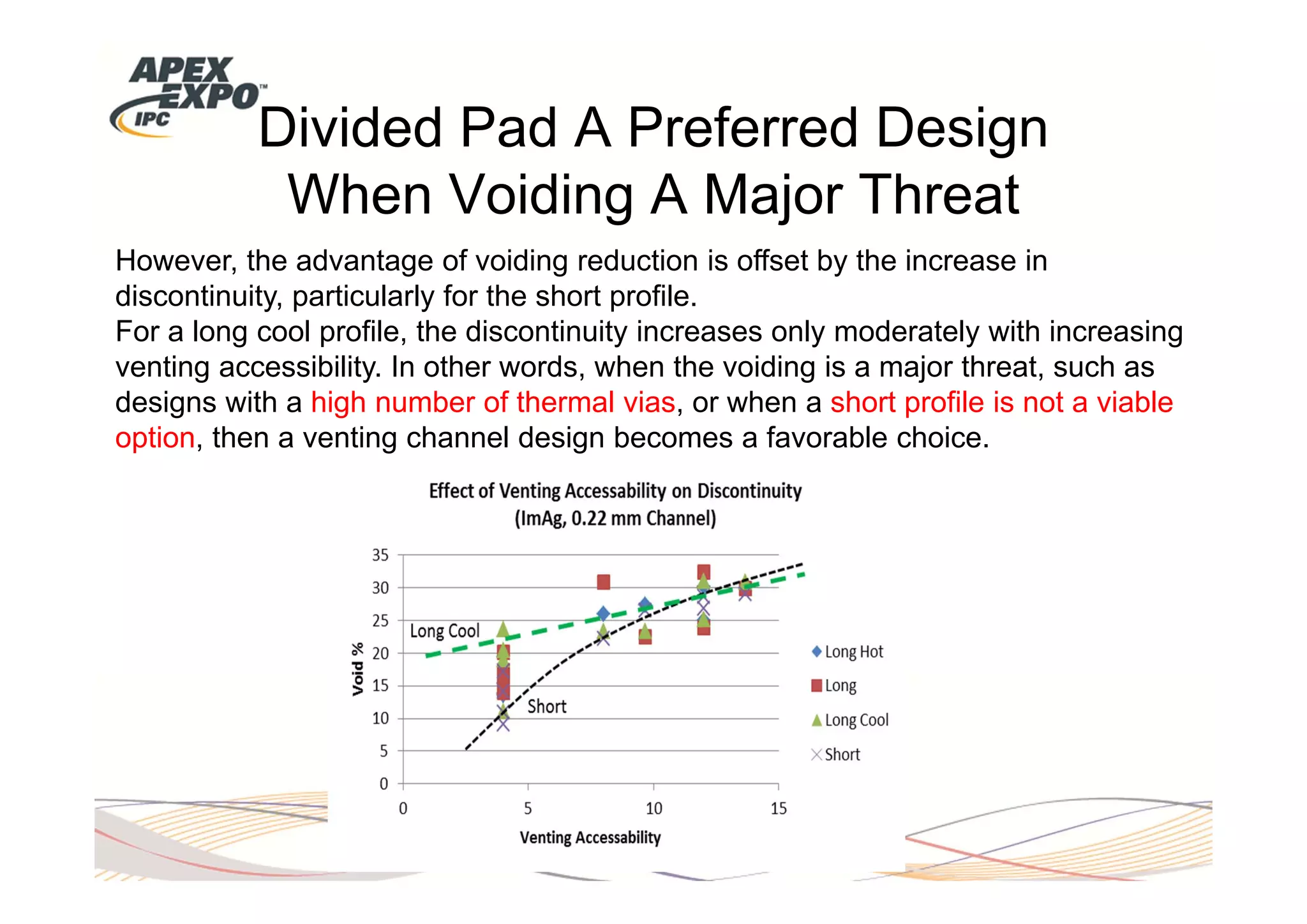
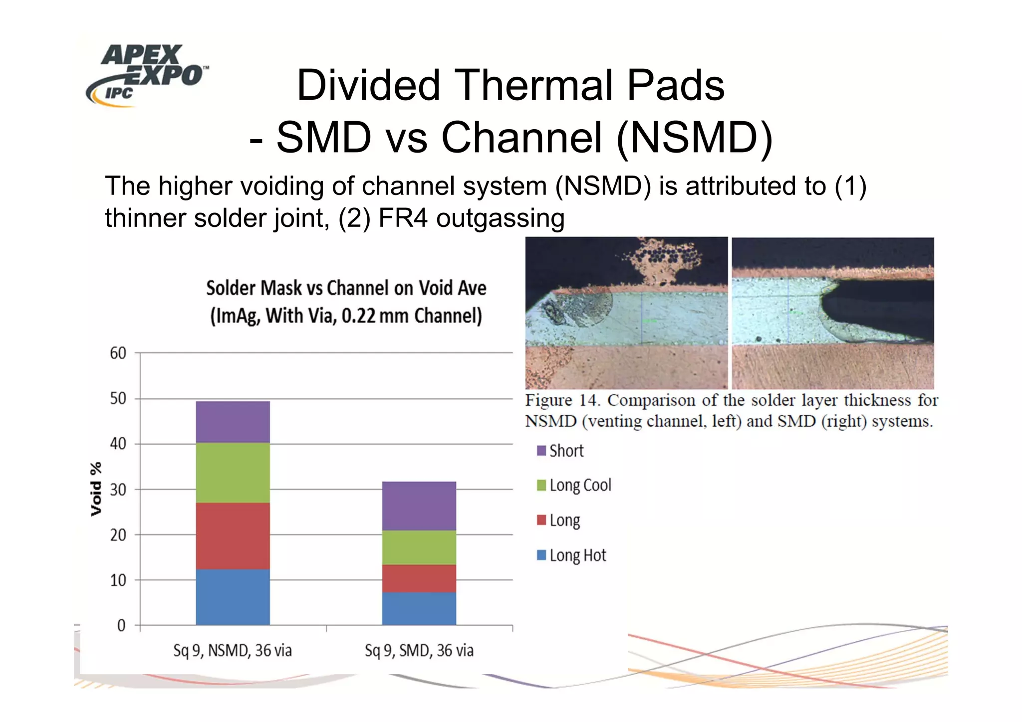
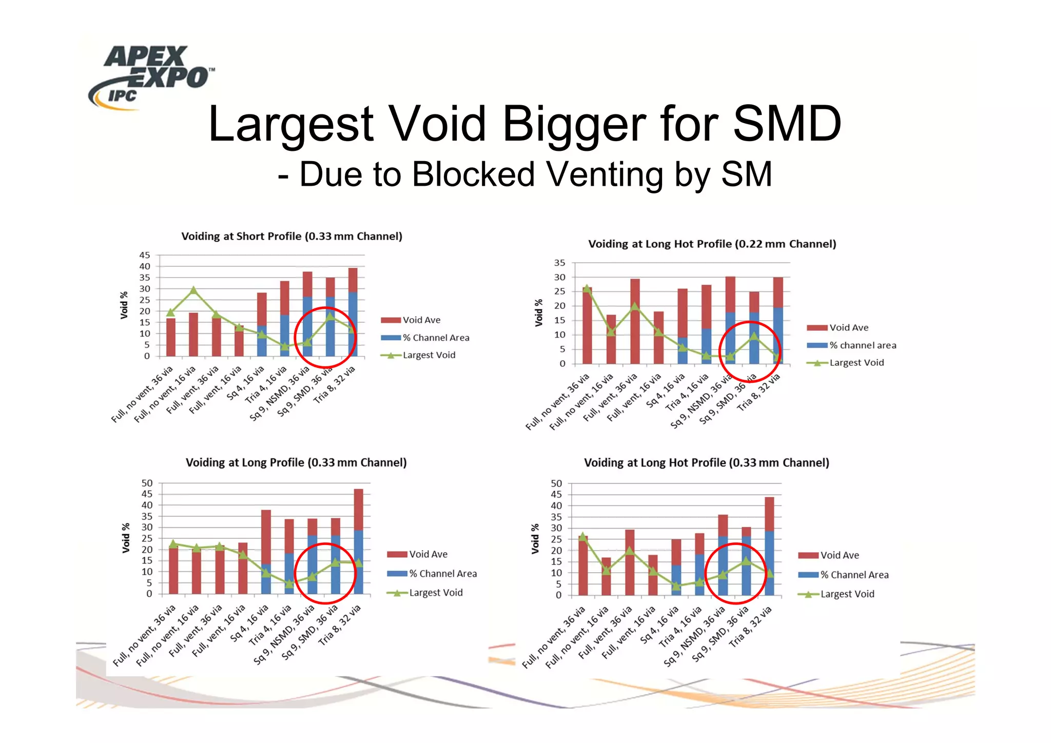
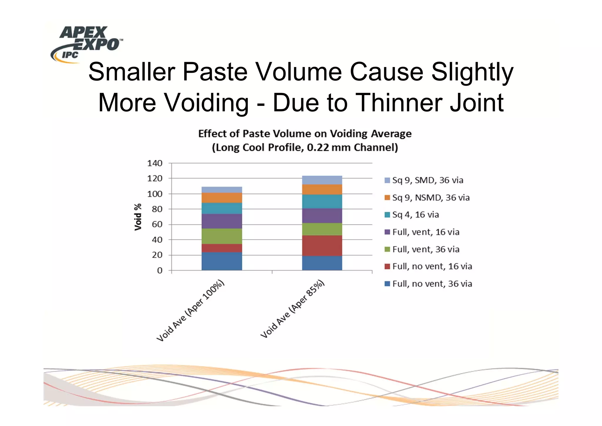
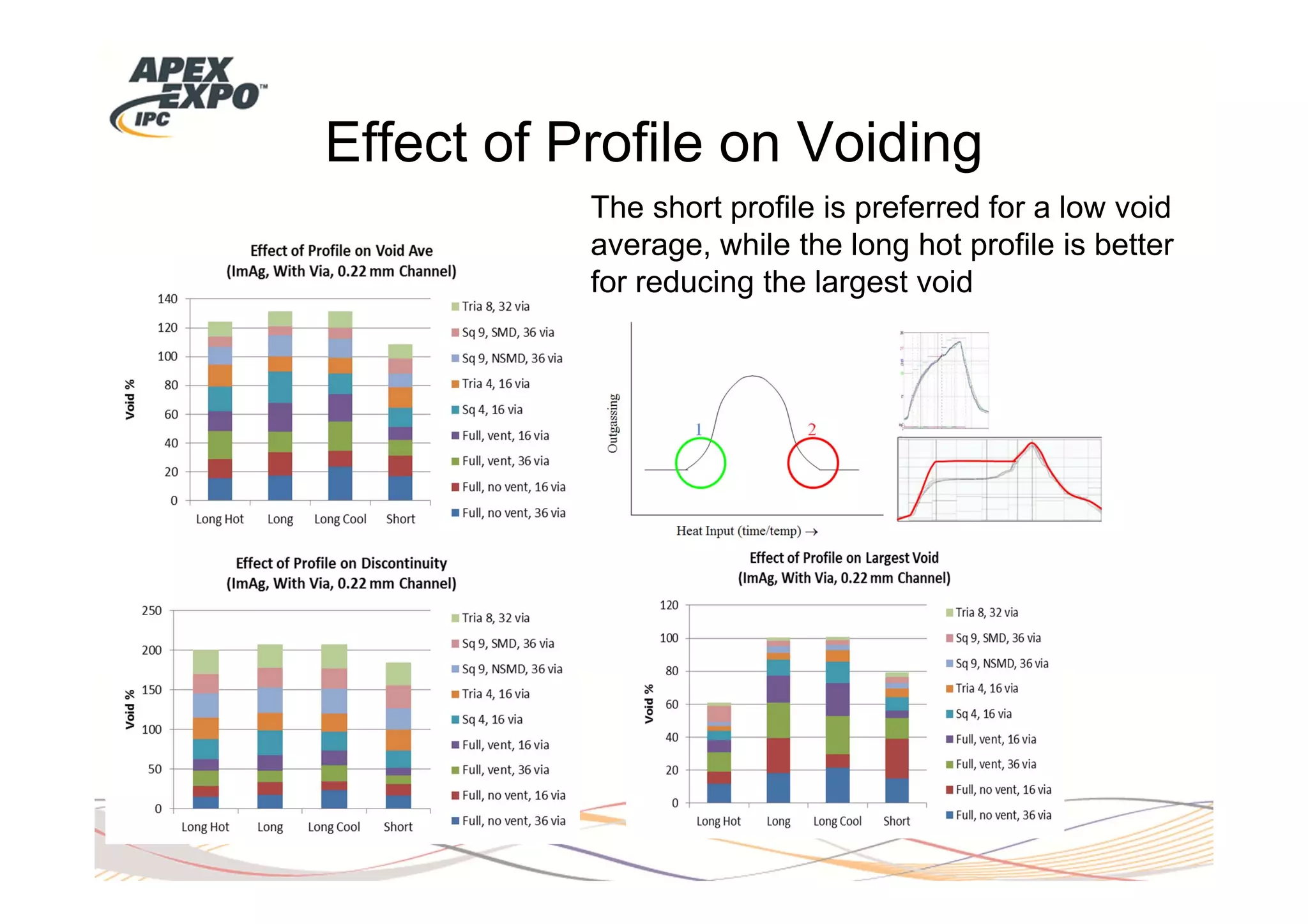
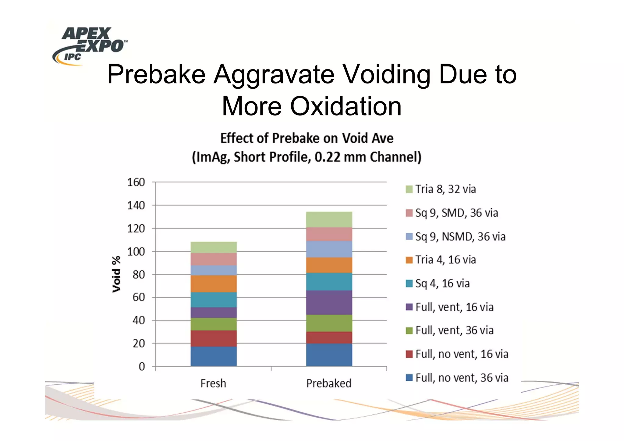
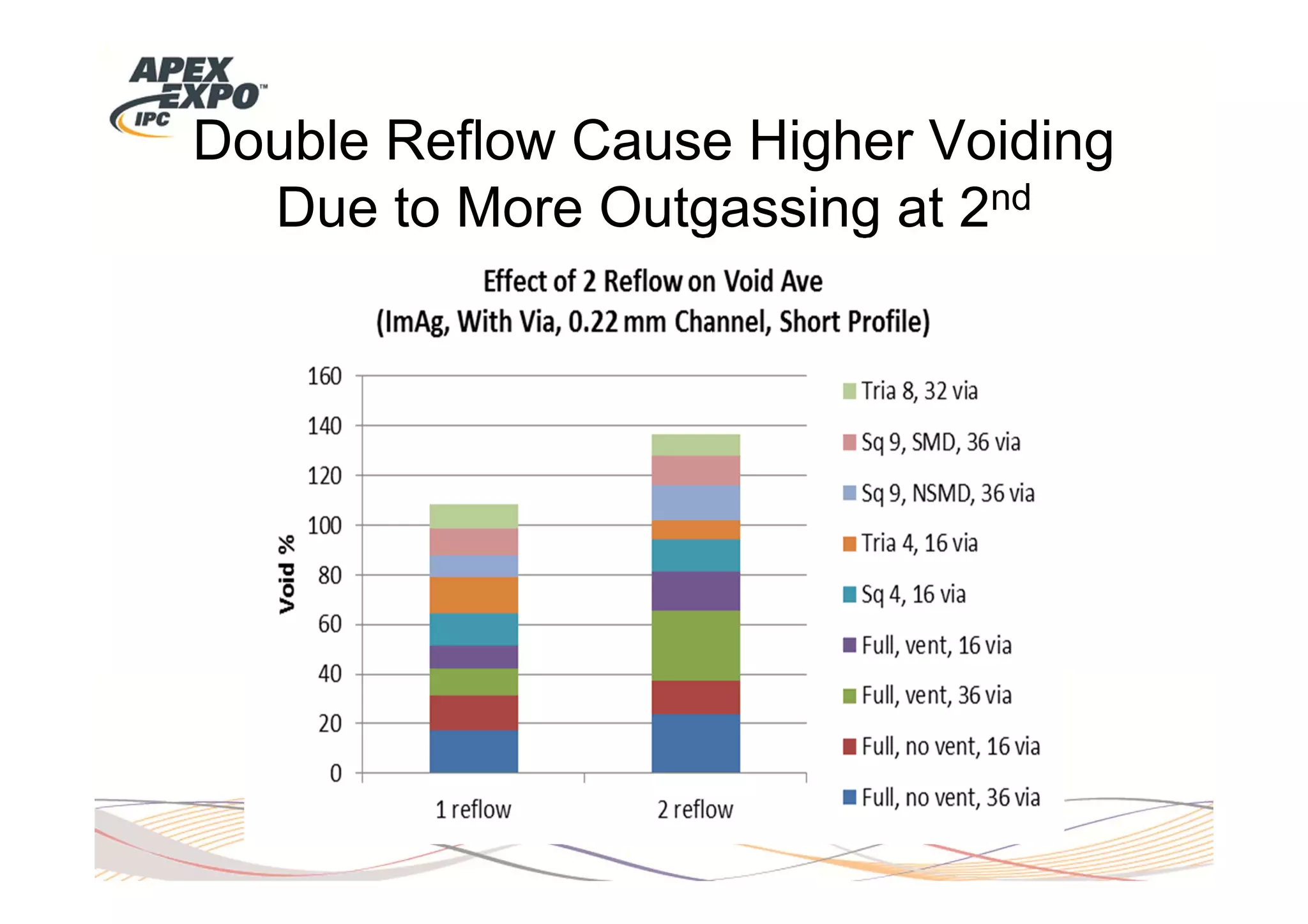
The document summarizes a study on pad design and process parameters to minimize voiding during QFN assembly. Key findings include: (1) Dividing large thermal pads into sub-units significantly reduces the largest voids while modestly increasing discontinuity; (2) Placing thermal vias peripherally or plugging vias is important when via number is high to control voiding; (3) Increased venting accessibility via sub-pad shape/number reduces voiding but compromises joint continuity.
The quad flat pack no lead or quad flat non-leaded (QFN) is one of the fastest growing package types in the electronics industry today. While the advantages of QFNs are well documented, concerns arise with its reliability and manufacturability. Acceptance of this package, especially in long-life, severe-environment, high-reliability applications, is currently limited. One of the most common drivers for reliability failures is inappropriate adoption of new technologies, such as the case with QFN. In this presentation, we will review and discuss QFN related reliability concerns and challenges, and propose Physics-of-Failure (PoF) based approaches to allow the confident introduction of QFN components into electronics products.
This training is very necessary to them who are working in Electronics manufacturing because Soldering process is the Heart of Electronics Industry, that's why this training is very important to employees.
Introduction to Surface Mount TechnologyABDUL MUNAFF
Surface Mount Technology (SMT) refers to a specific type of electronics assembly where electronic components are attached to the surface of a substrate (typically a printed circuit board).
SMT is a modern alternative to traditional thru-hole technology where components are attached to substrates by leads that passed through holes in the PCB.
Surface Mount components require less space so SMT is helpful in product miniaturization.
SMT Overview
SMT V/S THROUGH HOLE
Basic SMT process flow
Equipments used SMT Assembly
Through Hole Assembly & Soldering
ELECTROSTATIC DISCHARGE
RoHS
BTC: Bottom Termination Component or Biggest Technical Challenge?Cheryl Tulkoff
Bottom termination components (BTCs) are everywhere.
Despite the fact that these package types have been around since the mid ‘90s and have penetrated into almost every product market, companies still struggle to achieve the high yields the packages promise.
This presentation highlights the biggest mistakes and best practices to help conquer the BTC DEMInS: Design, Environment, Manufacturing, Inspection, and Stress.
PCBA Assembly Process Flow / PCB Assembly Manufacturing introduces the basic manufacturing process of PCBA / PCB assembly in different condition of component.It is about PCBA manufacture production.
This slide deck takes you through important elements of manula PCB inspection including some definitions, what makes a good inspector , what type of lighting is required to be able to see the important aspects of a PCB and the types of inspection aids. The slide deck ends with some real examples where the user is challenged to make a determination of defect/process indicator/acceptable of an electronics assembly in accordance with the IPC-A-610 and IPC-A-620 standards.
We provide totally solution for LED lighting SMT PCB assembly.
Worldwide Installation and on site support.
Factory (machine and lighting assembly) training.
This presentation is all about the working of Surface mount technology department of electronics industry. This is my personal experience at iljin electronics pvt. ltd. during my internship.
Pad Cratering: Prevention, Mitigation and Detection StrategiesCheryl Tulkoff
Pad cratering is defined as cracking which initiates within the laminate during a dynamic mechanical event such as In Circuit Testing (ICT), board depanelization, connector insertion, and other shock and vibration inducing activities.
During this tutorial, you'll learn about the key drivers, measurement and detection protocols, and preventive tactics for this serious but prevalent failure. Pad cratering was first recognized in BGA packages but newer leadless, bottom termination components are also vulnerable.
In-Service Corrosion Mapping—Challenges for the Chemical IndustryOlympus IMS
This presentation from ECNDT 2018 reviews the following topics:
Corrosion inspection—particularities of the chemical industry
Pitting detection in thin-wall components
Challenges of in-service inspection: high temperature
Results of accuracy tests with temperature variation
Fluxtrol's "Best Practice for Design and Manufacturing of Heat Treating Induc...Fluxtrol Inc.
With the use of good design practices, one can improve coil longevity and improve production quality. By eliminating failure points in the initial design, proper material selection, improved cooling and proper magnetic flux control, induction tooling life can be increased. Computer simulation has been proven to be an effective tool for predicting not only electromagnetic parameters of a designed system, but also heat patterns in a given part and in the induction coil itself. When a coil has magnetic flux controllers present, their influence may also be predicted by computer simulation. With an extensive library of published case studies in induction coil design and performance evaluations, we are confident with the use of these tools and proper coil geometries and implementation, production life and quality can be improved on most induction heat treating inductors. These design practices have been used by the authors for over 20 years with proven results. A case is examined of a CVJ stem hardening coil, in which the principles discussed can be applied to most other hardening coils.
Take a look into the reliability of plated through-holes and compare the impact of various amounts of copper plating in the through holes. Results of the thermal stress testing will be presented.
Learn about the critical factors of Heavy Copper Printed Circuit Boards for determining the appropriate Heavy Copper elements such as acceptable heat rise, copper thickness, hole-size, and if capable of support vias.
Taconic NF-30 for 77-79 GHz Safety and Reliability ApplicationsManfred Huschka
Due to the expected potential growth of 77/79 GHz ADAS (Advanced river-Assistance System) several non-PTFE (Polytetra Fluoro Ethylene) laminates are trying to find their way into designs. However from electrical and mechanical reliability points of view non-reinforced PTFE/Ceramic laminates still provide a leading edge
This paper discusses new developments in stencil laser and material technology and shows how these advancements, when combined, provide comparable and cost-effective alternatives to traditional electroformed stencils. The results are improved yields, cycle time reductions, and significant cost savings.
Similar to Pad design and process for voiding control at QFN assembly (20)
Search and Society: Reimagining Information Access for Radical FuturesBhaskar Mitra
The field of Information retrieval (IR) is currently undergoing a transformative shift, at least partly due to the emerging applications of generative AI to information access. In this talk, we will deliberate on the sociotechnical implications of generative AI for information access. We will argue that there is both a critical necessity and an exciting opportunity for the IR community to re-center our research agendas on societal needs while dismantling the artificial separation between the work on fairness, accountability, transparency, and ethics in IR and the rest of IR research. Instead of adopting a reactionary strategy of trying to mitigate potential social harms from emerging technologies, the community should aim to proactively set the research agenda for the kinds of systems we should build inspired by diverse explicitly stated sociotechnical imaginaries. The sociotechnical imaginaries that underpin the design and development of information access technologies needs to be explicitly articulated, and we need to develop theories of change in context of these diverse perspectives. Our guiding future imaginaries must be informed by other academic fields, such as democratic theory and critical theory, and should be co-developed with social science scholars, legal scholars, civil rights and social justice activists, and artists, among others.
PHP Frameworks: I want to break free (IPC Berlin 2024)Ralf Eggert
In this presentation, we examine the challenges and limitations of relying too heavily on PHP frameworks in web development. We discuss the history of PHP and its frameworks to understand how this dependence has evolved. The focus will be on providing concrete tips and strategies to reduce reliance on these frameworks, based on real-world examples and practical considerations. The goal is to equip developers with the skills and knowledge to create more flexible and future-proof web applications. We'll explore the importance of maintaining autonomy in a rapidly changing tech landscape and how to make informed decisions in PHP development.
This talk is aimed at encouraging a more independent approach to using PHP frameworks, moving towards a more flexible and future-proof approach to PHP development.
State of ICS and IoT Cyber Threat Landscape Report 2024 previewPrayukth K V
The IoT and OT threat landscape report has been prepared by the Threat Research Team at Sectrio using data from Sectrio, cyber threat intelligence farming facilities spread across over 85 cities around the world. In addition, Sectrio also runs AI-based advanced threat and payload engagement facilities that serve as sinks to attract and engage sophisticated threat actors, and newer malware including new variants and latent threats that are at an earlier stage of development.
The latest edition of the OT/ICS and IoT security Threat Landscape Report 2024 also covers:
State of global ICS asset and network exposure
Sectoral targets and attacks as well as the cost of ransom
Global APT activity, AI usage, actor and tactic profiles, and implications
Rise in volumes of AI-powered cyberattacks
Major cyber events in 2024
Malware and malicious payload trends
Cyberattack types and targets
Vulnerability exploit attempts on CVEs
Attacks on counties – USA
Expansion of bot farms – how, where, and why
In-depth analysis of the cyber threat landscape across North America, South America, Europe, APAC, and the Middle East
Why are attacks on smart factories rising?
Cyber risk predictions
Axis of attacks – Europe
Systemic attacks in the Middle East
Download the full report from here:
https://sectrio.com/resources/ot-threat-landscape-reports/sectrio-releases-ot-ics-and-iot-security-threat-landscape-report-2024/
JMeter webinar - integration with InfluxDB and GrafanaRTTS
Watch this recorded webinar about real-time monitoring of application performance. See how to integrate Apache JMeter, the open-source leader in performance testing, with InfluxDB, the open-source time-series database, and Grafana, the open-source analytics and visualization application.
In this webinar, we will review the benefits of leveraging InfluxDB and Grafana when executing load tests and demonstrate how these tools are used to visualize performance metrics.
Length: 30 minutes
Session Overview
-------------------------------------------
During this webinar, we will cover the following topics while demonstrating the integrations of JMeter, InfluxDB and Grafana:
- What out-of-the-box solutions are available for real-time monitoring JMeter tests?
- What are the benefits of integrating InfluxDB and Grafana into the load testing stack?
- Which features are provided by Grafana?
- Demonstration of InfluxDB and Grafana using a practice web application
To view the webinar recording, go to:
https://www.rttsweb.com/jmeter-integration-webinar
Accelerate your Kubernetes clusters with Varnish CachingThijs Feryn
A presentation about the usage and availability of Varnish on Kubernetes. This talk explores the capabilities of Varnish caching and shows how to use the Varnish Helm chart to deploy it to Kubernetes.
This presentation was delivered at K8SUG Singapore. See https://feryn.eu/presentations/accelerate-your-kubernetes-clusters-with-varnish-caching-k8sug-singapore-28-2024 for more details.
Connector Corner: Automate dynamic content and events by pushing a buttonDianaGray10
Here is something new! In our next Connector Corner webinar, we will demonstrate how you can use a single workflow to:
Create a campaign using Mailchimp with merge tags/fields
Send an interactive Slack channel message (using buttons)
Have the message received by managers and peers along with a test email for review
But there’s more:
In a second workflow supporting the same use case, you’ll see:
Your campaign sent to target colleagues for approval
If the “Approve” button is clicked, a Jira/Zendesk ticket is created for the marketing design team
But—if the “Reject” button is pushed, colleagues will be alerted via Slack message
Join us to learn more about this new, human-in-the-loop capability, brought to you by Integration Service connectors.
And...
Speakers:
Akshay Agnihotri, Product Manager
Charlie Greenberg, Host
Let's dive deeper into the world of ODC! Ricardo Alves (OutSystems) will join us to tell all about the new Data Fabric. After that, Sezen de Bruijn (OutSystems) will get into the details on how to best design a sturdy architecture within ODC.
Kubernetes & AI - Beauty and the Beast !?! @KCD Istanbul 2024Tobias Schneck
As AI technology is pushing into IT I was wondering myself, as an “infrastructure container kubernetes guy”, how get this fancy AI technology get managed from an infrastructure operational view? Is it possible to apply our lovely cloud native principals as well? What benefit’s both technologies could bring to each other?
Let me take this questions and provide you a short journey through existing deployment models and use cases for AI software. On practical examples, we discuss what cloud/on-premise strategy we may need for applying it to our own infrastructure to get it to work from an enterprise perspective. I want to give an overview about infrastructure requirements and technologies, what could be beneficial or limiting your AI use cases in an enterprise environment. An interactive Demo will give you some insides, what approaches I got already working for real.
Transcript: Selling digital books in 2024: Insights from industry leaders - T...BookNet Canada
The publishing industry has been selling digital audiobooks and ebooks for over a decade and has found its groove. What’s changed? What has stayed the same? Where do we go from here? Join a group of leading sales peers from across the industry for a conversation about the lessons learned since the popularization of digital books, best practices, digital book supply chain management, and more.
Link to video recording: https://bnctechforum.ca/sessions/selling-digital-books-in-2024-insights-from-industry-leaders/
Presented by BookNet Canada on May 28, 2024, with support from the Department of Canadian Heritage.
Slack (or Teams) Automation for Bonterra Impact Management (fka Social Soluti...Jeffrey Haguewood
Sidekick Solutions uses Bonterra Impact Management (fka Social Solutions Apricot) and automation solutions to integrate data for business workflows.
We believe integration and automation are essential to user experience and the promise of efficient work through technology. Automation is the critical ingredient to realizing that full vision. We develop integration products and services for Bonterra Case Management software to support the deployment of automations for a variety of use cases.
This video focuses on the notifications, alerts, and approval requests using Slack for Bonterra Impact Management. The solutions covered in this webinar can also be deployed for Microsoft Teams.
Interested in deploying notification automations for Bonterra Impact Management? Contact us at sales@sidekicksolutionsllc.com to discuss next steps.
Pad design and process for voiding control at QFN assembly
1. Pad Design and Process for
Voiding Control at QFN
Assembly
Derrick Herron, Dr. Yan Liu, and
Dr. Ning-Cheng Lee
Indium Corporation
2. Background
• QFN prevailing due to (1) small size & light weight; (2) easy
PCB trace routing due to the use of perimeter I/O pads; (3)
reduced lead inductance; and (4) good thermal and
electrical performance due to the adoption of exposed
copper die-pad technology
• Voiding is issue at SMT assembly due to the large coverage
area, large number of thermal via, and low standoff
• Both design and process were studied for minimizing and
controlling the voiding
3. Parameters Studied
QFN with 68 pads, 10mm x 10mm, 0.5mm
pitch, daisy-chained, Sn surface finish
Parameter Sub parameter Layers
Thermal via number 0, 16, 32, 36
Peripheral venting for full With and without
thermal pad
Thermal Pad on PCB Dividing method Solder mask, venting
channel (0.22 & 0.33 mm)
Thermal sub-pad shape Square, triangle
Thermal sub-pad number 1, 4, 8, 9
Stencil Aperture 85%, 100%
Reflow profile Short, long cool, long, long
Heat History hot
Other heat treatment Prebake, 1 reflow, 2 reflow
6. Voiding Examples
The drastic
difference in
voiding behavior
between the two
sets demonstrates 0.22 mm
the tremendous
impact of design
and process
conditions
0.33 mm
6 INDIUM CORPORATION
CONFIDENTIAL
7. Definition of 3 Voiding Properties
Property Definition
Discontinuity Percentage of area under the
QFN thermal pad where the
vertical metal continuity from
QFN to PCB surface is
interrupted
Void Average Average of multiple QFNs for
void area percentage within
the metallic pad of QFN
Largest Void The largest void measured for
a category of QFN joints
8. Individual Voiding Data Set
Dividing the thermal
pads into sub-units
results in an abrupt drop
in the largest void but an
increase in discontinuity
Net effect: a reduction in
the uncontrollable,
harmful large voids,
replacing it with a
controlled, even
distribution of
8 INDIUM CORPORATION
discontinuity CONFIDENTIAL
9. Dividing Desired for High Via No.
When the thermal via number is high, the discontinuity of a full
pad becomes comparable with that of a divided pad, and the
sporadic occurrence of large voids becomes a distinct
disadvantage of the full pad design
36 36 36
36
10. Thermal Via Aggravate Voiding
Propensity of voids at the
via locations is particularly
high for full pad solder
joints
Thus, voiding increase w
increasing via no.
If high via no. is needed, plugging the via
is the best option
11. Divided Pads with Peripheral Via Not
Sensitive to Via No. on Voiding
The number of thermal via bears no relation with voiding for
divided pads. This is attributed to the peripheral location of thermal
via for those divided pads. If plugging the thermal via is not an
option, design the thermal via at peripheral locations whenever
possible.
16 36 16 36
16 36 16 36
13. Increase Channel Width Has No Effect on Void Ave,
but Increase Channel Area & Discontinuity
14. Calculated Venting Accessibility of
Thermal Pad Designs
Venting Accessibility: Perimeter length per
unit area of metal pad
Thermal pad Venting
design accessibility
Full pad 4
Square 4 8
Triangle 4 9.66
Square 9 12
Triangle 8 13.66
15. Venting Accessibility Effect on
Largest Void & Void Average
With increasing venting accessibility, the void average and
largest void decrease readily
16. Divided Pad A Preferred Design
When Voiding A Major Threat
However, the advantage of voiding reduction is offset by the increase in
discontinuity, particularly for the short profile.
For a long cool profile, the discontinuity increases only moderately with increasing
venting accessibility. In other words, when the voiding is a major threat, such as
designs with a high number of thermal vias, or when a short profile is not a viable
option, then a venting channel design becomes a favorable choice.
17. Divided Thermal Pads
- SMD vs Channel (NSMD)
The higher voiding of channel system (NSMD) is attributed to (1)
thinner solder joint, (2) FR4 outgassing
20. Effect of Profile on Voiding
The short profile is preferred for a low void
average, while the long hot profile is better
for reducing the largest void
23. Discussion (1)
• Prospect of thermal via
– When mechanical drilled thermal via (0.3mm drill
diam/1.2mm pitch) evolve to microvia, the via
pitch decreases, thermal via density may
becomes higher, & voiding may worsen
• How much voiding is too much?
– Voiding up to 50% or even 60% OK
– But, the largest void should be < pitch
• What is less evil?
– High void or uneven size distribution?
24. Discussion (2)
• Patterned solder paste common approach
– Multiple opens
– 50-80% coverage
– 0.15-0.3 mm spacing
– But, still has voiding issue
• Permanent venting channel desired
– Higher discontinuity may be acceptable, since
50% voiding acceptable
– Controlled even distribution of discontinuity better
25. Discussion (3)
• Venting or being vented?
– Remove metal to form channel less obstruction on
vending
– But, allow FR4 to outgass moisture from channel
• What is next?
– Thin solder mask for SMD thermal pad
• Short vs long hot
– Long hot more consistent, due to a wider reflow
process window
– Price – slightly higher void average
26. Conclusion (1)
• Plugging is most effective in reducing voiding
• For unplugged via situations, a full thermal pad is desired for
a low no. of via
• For a high no. of thermal via, a divided thermal pad is
preferred, due to better venting capability
• Placement of thermal via at the perimeter lessens voiding
caused by via
• A wider venting channel has a negligible effect on voiding,
but reduces joint continuity
• For a divided thermal pad, a SMD system is more favorable
than a channel (NSMD) system, with the latter suffering more
voiding due to a thinner solder joint and possibly board
outgassing
27. Conclusion (2)
• Performance of a divided thermal pad is dictated by venting
accessibility, not by the shape
• Voiding decreases with increasing venting accessibility,
although the introduction of a channel area compromises
the continuity of the solder joint
• Reduced solder paste volume causes more voiding
• A short profile and a long hot profile are most promising in
reducing the voiding
• Voiding behavior of the QFN is similar to typical SMT
voiding and increases with pad oxidation and further reflow