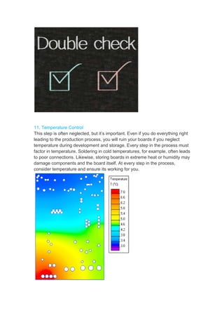
12 Biggest PCB Mistakes – From Layout to
Manufacturing
Printed Circuit Boards (PCBs) are without a doubt central to all electronics. As
technology advances, however, PCBs must be made faster and smaller than
ever before. Before you get busy, make sure you nip sloppy PCB production
in the bud, before it costs you big bucks. Read on to discover the 12 biggest
PCB development mistakes and how to avoid them.
Layout
1. Improper Planning
Have you ever heard “proper planning prevents poor performance?” It’s true.
There’s a reason we consider poor planning the number one PCB
development mistake. There is no substitute for proper PCB planning. It can
save you time and energy. If you build it wrong, you will have to spend
additional resources to go back and fix it. How do you plan properly? Consider
numbers 2-6 on our list before you physically begin building. You’ll be thankful
you did.
2. Incorrect Design
There is an infinite number
mind when designing the
need to add on in the future,
grid array (BGA), which
enable you to build upon
incorporate copper, you’d
Whatever your function,
3. Improper Board Size
It’s much easier to begin
project you’re working on
to have to add on in the
Stringing multiple boards
and connectivity issues.
future function so you save
number of layout possibilities with PCBs. Keep
the form. For example, if there’s a good change
future, you may want to consider something
can help conserve space on an existing
upon that design in the future. If your design
you’d be best going with a polygon-style design.
function, choose the right form.
begin with the right size first. Although the portion
on now may only require a small board, if
the future, you’re better off getting the larger
boards together may be difficult due to potential
issues. Plan adequately not only for current function
save yourself time and money.
Keep function in-
change you’ll
something like a ball
board to
must
design.
portion of the
you’re going
larger board now.
potential circuitry
function but
4. Failing to Group Like Items
Grounping your PCB is a critical part of production. Grouping like items will
not only help you keep your trace lengths short (another important element of
design), but it will also help you avoid circuitry issues, ease testing and make
error correction much more simple.
5. Software, Software, Software
We know you can design a PCB from scratch, but why would you want to
when you can use software? Software makes your life easier. Electronic
Design Automation gives you recommendations for the best layout to choose
and other programs may suggest the best materials to use, based on
prospective board function. Software won’t do all of the thinking for you, but it
sure does help.
6. Using the Silk Screen
A huge ally when creating
used properly, it’s a great
PCB before construction,
maintain best practices.
difficult to know where connectors
full words as descriptors
Building
Once you’re done planning,
out of the water, however.
mistakes. When done well,
7. Poorly-Constructed Via
This issue is one of the
boards now require via-
to breakouts in your ground
power travels between boards
your ground plane. If you
cap or mask it and test it
save you time in the long
Screen Improperly
creating a design for a PCB board is the silk screen.
great tool that allows you to map out all aspects
construction, including circuitry planning. However, be
practices. When used improperly, the silk screen can
connectors and components are supposed
descriptors when possible, or keep a key of your symbols
planning, you can begin building your board. You’re
however. Building is another area where people
well, however, you can build PCBs faster than
Via-in-Pad
biggest detriments to proper PCB development.
-in-pads, but when soldered incorrectly, vias
ground plane. This creates a larger circuitry
boards instead of connectors and components.
you suspect you have a shaky via-in-pad on
it again. It may slow down production now,
long run.
screen. When
aspects of your
be careful and
can make it
supposed to go. Use
symbols nearby.
You’re still not
people make costly
than ever.
development. Many
vias can lead
issue, as
components. Test
on your board,
now, but it’ll
8. Using the Wrong Material
Although this mistake may
constructed using various
building your board, and
start building. If you’re building
phenolic or paper materials.
epoxy or glass cloth. Also,
Keep this in mind. If you’re
an area with a lot of humidity,
9. Too Lazy to Test It
If there’s one habit you begin
your prototype. Assuming
function in perfect accordance
is asking for trouble. We
Materials
may seem like a novice move, it happens.
various materials. Know the purpose for which
and which materials are best for that design,
building an FR-2 grade, single-sided PCB,
materials. Anything more complex, however, should
Also, different materials have different temperaments.
you’re building a simple design that needs to
humidity, it may be worth it to go with epoxy.
begin to change, it should be the frequency
Assuming your board is grounded and that circuits
accordance with their potential ground paths and
We know it takes time to test your board, but
PCBs can be
which you are
design, before you
PCB, you can use
should use
temperaments.
to hold up in
epoxy.
frequency you test
circuits will
and voltages
but it’ll take
more time to find and correct an error as time goes on. Test it now. Every
design has an issue, keep that thought in mind.
Manufacturing
So you properly planned and built your board. Things couldn’t still go wrong,
could they? Wrong! They can and they do. These are the three mistakes to
avoid.
10. Failing to Double Crunch the Numbers
We’ve all felt the pressure of an upcoming product deadline. You’re sweating,
over-caffeinated and running on lack of sleep. We know you’re an engineer,
but don’t let your ego cost your company huge amounts of money due to an
error. Always double-check your numbers before sending your model to
production. This includes testing your board, ensuring the size is in line with
your client’s specifications and double-checking your design is ideal for the
intended function. It’s always better to have one model that needs to be
reworked than a thousand. Rewind to #1 in this list… proper planning. Never
jump the gun when sending out the design.
11. Temperature Control
This step is often neglected, but it’s important. Even if you do everything right
leading to the production process, you will ruin your boards if you neglect
temperature during development and storage. Every step in the process must
factor in temperature. Soldering in cold temperatures, for example, often leads
to poor connections. Likewise, storing boards in extreme heat or humidity may
damage components and the board itself. At every step in the process,
consider temperature and ensure its working for you.
12. Communicate
Building PCBs can be fun, if you create functional boards at the end of the
grueling process. So you designed your board well and followed best
practices during production – you’re in the clear, right? Not always. Ensure
you properly communicate with your clients at all times. It sounds simple, but
what’s said isn’t always what’s heard. Your finished product can be rejected.
Save yourself a step by making sure you’re creating what your client wants at
every step in the process, so you can move onto more fun things, like making
a paper airplane machine gun.
LISA LIU JINGWEN
lisa@jaapson-pcb.com
www.jaapsonpcb.com
skype: jaapsoncircuits
JAAPSON, Expert in HDI Multi-layer PCB manufacturing
(This article is from Mr.Cabe Atwell)

12 Biggest PCB Mistakes – from Layout to Manufacturing

  • 1.
    12 Biggest PCBMistakes – From Layout to Manufacturing Printed Circuit Boards (PCBs) are without a doubt central to all electronics. As technology advances, however, PCBs must be made faster and smaller than ever before. Before you get busy, make sure you nip sloppy PCB production in the bud, before it costs you big bucks. Read on to discover the 12 biggest PCB development mistakes and how to avoid them. Layout 1. Improper Planning Have you ever heard “proper planning prevents poor performance?” It’s true. There’s a reason we consider poor planning the number one PCB development mistake. There is no substitute for proper PCB planning. It can save you time and energy. If you build it wrong, you will have to spend additional resources to go back and fix it. How do you plan properly? Consider numbers 2-6 on our list before you physically begin building. You’ll be thankful you did.
  • 2.
    2. Incorrect Design Thereis an infinite number mind when designing the need to add on in the future, grid array (BGA), which enable you to build upon incorporate copper, you’d Whatever your function, 3. Improper Board Size It’s much easier to begin project you’re working on to have to add on in the Stringing multiple boards and connectivity issues. future function so you save number of layout possibilities with PCBs. Keep the form. For example, if there’s a good change future, you may want to consider something can help conserve space on an existing upon that design in the future. If your design you’d be best going with a polygon-style design. function, choose the right form. begin with the right size first. Although the portion on now may only require a small board, if the future, you’re better off getting the larger boards together may be difficult due to potential issues. Plan adequately not only for current function save yourself time and money. Keep function in- change you’ll something like a ball board to must design. portion of the you’re going larger board now. potential circuitry function but
  • 3.
    4. Failing toGroup Like Items Grounping your PCB is a critical part of production. Grouping like items will not only help you keep your trace lengths short (another important element of design), but it will also help you avoid circuitry issues, ease testing and make error correction much more simple. 5. Software, Software, Software We know you can design a PCB from scratch, but why would you want to when you can use software? Software makes your life easier. Electronic Design Automation gives you recommendations for the best layout to choose and other programs may suggest the best materials to use, based on prospective board function. Software won’t do all of the thinking for you, but it sure does help.
  • 4.
    6. Using theSilk Screen A huge ally when creating used properly, it’s a great PCB before construction, maintain best practices. difficult to know where connectors full words as descriptors Building Once you’re done planning, out of the water, however. mistakes. When done well, 7. Poorly-Constructed Via This issue is one of the boards now require via- to breakouts in your ground power travels between boards your ground plane. If you cap or mask it and test it save you time in the long Screen Improperly creating a design for a PCB board is the silk screen. great tool that allows you to map out all aspects construction, including circuitry planning. However, be practices. When used improperly, the silk screen can connectors and components are supposed descriptors when possible, or keep a key of your symbols planning, you can begin building your board. You’re however. Building is another area where people well, however, you can build PCBs faster than Via-in-Pad biggest detriments to proper PCB development. -in-pads, but when soldered incorrectly, vias ground plane. This creates a larger circuitry boards instead of connectors and components. you suspect you have a shaky via-in-pad on it again. It may slow down production now, long run. screen. When aspects of your be careful and can make it supposed to go. Use symbols nearby. You’re still not people make costly than ever. development. Many vias can lead issue, as components. Test on your board, now, but it’ll
  • 5.
    8. Using theWrong Material Although this mistake may constructed using various building your board, and start building. If you’re building phenolic or paper materials. epoxy or glass cloth. Also, Keep this in mind. If you’re an area with a lot of humidity, 9. Too Lazy to Test It If there’s one habit you begin your prototype. Assuming function in perfect accordance is asking for trouble. We Materials may seem like a novice move, it happens. various materials. Know the purpose for which and which materials are best for that design, building an FR-2 grade, single-sided PCB, materials. Anything more complex, however, should Also, different materials have different temperaments. you’re building a simple design that needs to humidity, it may be worth it to go with epoxy. begin to change, it should be the frequency Assuming your board is grounded and that circuits accordance with their potential ground paths and We know it takes time to test your board, but PCBs can be which you are design, before you PCB, you can use should use temperaments. to hold up in epoxy. frequency you test circuits will and voltages but it’ll take
  • 6.
    more time tofind and correct an error as time goes on. Test it now. Every design has an issue, keep that thought in mind. Manufacturing So you properly planned and built your board. Things couldn’t still go wrong, could they? Wrong! They can and they do. These are the three mistakes to avoid. 10. Failing to Double Crunch the Numbers We’ve all felt the pressure of an upcoming product deadline. You’re sweating, over-caffeinated and running on lack of sleep. We know you’re an engineer, but don’t let your ego cost your company huge amounts of money due to an error. Always double-check your numbers before sending your model to production. This includes testing your board, ensuring the size is in line with your client’s specifications and double-checking your design is ideal for the intended function. It’s always better to have one model that needs to be reworked than a thousand. Rewind to #1 in this list… proper planning. Never jump the gun when sending out the design.
  • 7.
    11. Temperature Control Thisstep is often neglected, but it’s important. Even if you do everything right leading to the production process, you will ruin your boards if you neglect temperature during development and storage. Every step in the process must factor in temperature. Soldering in cold temperatures, for example, often leads to poor connections. Likewise, storing boards in extreme heat or humidity may damage components and the board itself. At every step in the process, consider temperature and ensure its working for you.
  • 8.
    12. Communicate Building PCBscan be fun, if you create functional boards at the end of the grueling process. So you designed your board well and followed best practices during production – you’re in the clear, right? Not always. Ensure you properly communicate with your clients at all times. It sounds simple, but what’s said isn’t always what’s heard. Your finished product can be rejected. Save yourself a step by making sure you’re creating what your client wants at every step in the process, so you can move onto more fun things, like making a paper airplane machine gun. LISA LIU JINGWEN lisa@jaapson-pcb.com www.jaapsonpcb.com skype: jaapsoncircuits JAAPSON, Expert in HDI Multi-layer PCB manufacturing (This article is from Mr.Cabe Atwell)