
More Related Content
What's hot
What's hot (20)
Similar to Project report on design & implementation of high speed carry select adder
Similar to Project report on design & implementation of high speed carry select adder (20)
Recently uploaded
Recently uploaded (20)
Project report on design & implementation of high speed carry select adder
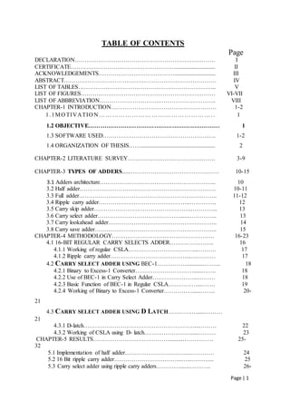
- 1. Page | 1 TABLE OF CONTENTS Page DECLARATION……………………………………………………………… I CERTIFICATE………………………………………………........................... II ACKNOWLEDGEMENTS…………………………………............................ III ABSTRACT…………………………………………………………………… IV LIST OF TABLES…………………………………………………………….. V LIST OF FIGURES…………………………………………………………… VI-VII LIST OF ABBREVIATION………………………….……………………….. VIII CHAPTER-1 INTRODUCTION……………………………………………… 1-2 1.1MO TIVATIO N …………………………………………….. 1 1.2 OBJECTIVE………………………………………………………… 1 1.3 SOFTWARE USED…………………………………………………. 1-2 1.4 ORGANIZATION OF THESIS……................................................... 2 CHAPTER-2 LITERATURE SURVEY……………………………………… 3-9 CHAPTER-3 TYPES OF ADDERS......……………………………………… 10-15 3.1 Adders architecture…………………………………………………... 10 3.2 Half adder……………………………………………………………. 10-11 3.3 Full adder…………………………………………………………….. 11-12 3.4 Ripple carry adder………………………………………..………….. 12 3.5 Carry skip adder…………………………………………..………….. 13 3.6 Carry select adder…………………………………….......………….. 13 3.7 Carry lookahead adder……………………………………………….. 14 3.8 Carry save adder………………………………………….………….. 15 CHAPTER-4 METHODOLOGY……………………….….………………… 16-23 4.1 16-BIT REGULAR CARRY SELECTS ADDER………………….. 16 4.1.1 Working of regular CSLA……………………………....……… 17 4.1.2 Ripple carry adder…………………………………...….……… 17 4.2 CARRY SELECT ADDER USING BEC-1……………............……... 18 4.2.1 Binary to Excess-1 Converter………………………….....…….. 18 4.2.2 Use of BEC-1 in Carry Select Adder…………………...……… 18 4.2.3 Basic Function of BEC-1 in Regular CSLA……………...……. 19 4.2.4 Working of Binary to Excess-1 Converter…………….....…….. 20- 21 4.3 CARRY SELECT ADDER USING D LATCH…………….....……… 21 4.3.1 D-latch…………………………………………………...……… 22 4.3.2 Working of CSLA using D- latch…………………….....……… 23 CHAPTER-5 RESULTS………………………………….........……………. 25- 32 5.1 Implementation of half adder…………………….……....………… 24 5.2 16 Bit ripple carry adder……………………………..…...………... 25 5.3 Carry select adder using ripple carry adders………….......……….. 26-
- 2. Page | 2 27 5.4 Carry select adder using BEC-1 technique…………........………... 28- 29 5.5 Carry select adder using D latch………………………....………. . 30- 32 5.6 Comparison…………………………………………….....……….. 32 CHAPTER-6 CONCLUSION & FUTURE SCOPE ………....…………..... 33 REFERENCES……………………………………………………………… 34
- 3. Page | 3 CHAPTER-1 INTRODUCTION Area and power reduction in data path logic systems are the main area of research in VLSI system design. High speed addition and multiplication has always been a fundamental requirement of high-performance processors and systems. 1.1MOTIVATION: Addition is the most common and often used arithmetic operation on microprocessor, digital signal processor, especially digital computers. Also, it serves as a building block for synthesis all other arithmetic operations. Therefore, regarding the efficient implementation of an arithmetic unit, the binary adder structures become a very critical hardware unit. In digital adders, the speed of addition is limited by the time required to propagate a carry through the adder. The sum for each bit position in an elementary adder is generated sequentially only after the previous bit position has been summed and a carry propagated into the next position. The major speed limitation in any adder is in the production of carries and many authors have considered the addition problem. The carry select adder is used in many computational systems to moderate the problem of carry propagation delay by independently generating multiple carries and then select a carry to generate the sum. 1.2 OBJECTIVE: Our main objective to reduce the area, delay & power consumption of carry select adder. The carry select adder using d latch has less delay and area efficient as compared to conventional carry select adder and carry select adder using bec-1 technique. 1.3 SOFTWARE USED: XILINX 14.1 ISE DESIGN SUITE is used to simulate and synthesize the circuit of various techniques of carry select adder.Xilinx ISE (Integrated Synthesis Environment) a
- 4. Page | 4 software tool produced by Xilinx for synthesis and analysis of HDL designs, enabling the developer to synthesize("compile") their designs, perform timing analysis, examine RTL diagrams, simulate a design's reaction to different stimuli, and configure the target device with the programmer. Synthesis Tool: to synthesis the design or a circuit we are using Synthesize XST. Simulator: to simulate the circuit we are using ISIM Simulator. 1.4 ORGANIZATION OF THESIS: This thesis report contains six chapters. The second chapter encloses the literature review which discusses the certain parameter like area delay and power consumption of various paper of carry select adder. The third Chapter enclose the type of adders and discuss the working of various adders like full adder, half adder, carry save adder, carry look ahead adder, carry save adder, ripple carry adder and carry select adder. In fourth chapter results are discussed the various methodology of carry select adder Carry select adder using ripple carry adder. Carry select adder using bec-1 technique. Carry select adder using D – latch. The fifth chapter describe results of various technique of carry select adder. The sixth chapter discuss conclusion and future work of a project.
- 5. Page | 3 CHAPTER - 2 LITERATURE SURVEY A number of circuit techniques have been developed to reduce the delay, area and power consumption in the regular carry select adder circuit. In this section we present an overview of some significant techniques which are used to reduce the delay,area and power consumption. 1.Chang and Hsiao 1998 propose that instead of using dual carry ripple adder a carry select adder scheme using an add one circuit to replace one carry ripple adder. In this technique one carry ripple adder is used instead of using dual carry ripple adder to enhance the area,power and delay. 2.Youngwood Kim and Lee Sup Kim 2001 introduces a multiplexer based add one circuit is proposed to reduce the area with negligible speed penalty: A carry-select adder can be implemented by using single ripple carry adder and an add- one circuit instead of using dual ripple-carry adders. This paper proposes a new add-one circuit using the first zero finding circuit and multiplexers to reduce the area and power with no speed penalty. For bit length n = 64, this new carry-select adder requires 38 percent fewer transistors than the dual ripple-carry carry-select adder and 29 percent fewer transistors than Chang’s carry-select adder using single ripple carry adder [1]. This new 64b adder has 3.45ns delay time at 2.5V power supply using a 0.25um CMOS technology. Compared to the conventional and Chang’s CSA, the proposed adder required 38% and 29% fewer transistors, respectively. Fewer transistors results less area and less power. The power consumption of proposed CSLA is estimated to be only 75% of the conventional CSLA.
- 6. Page | 4 3. Ramkumar and Harish 2012 propose BEC technique which is a simple and efficient gate level modification to significantly reduce the area and power of square root CSLA. This work uses a simple and efficient gate-level modification to significantly reduce the area and power of the CSLA. Based on this modification 8-, 16-, 32-, and 64-b square- root CSLA (SQRT CSLA) architecture have been developed and compared with the regular SQRT CSLA architecture. The proposed design has reduced area and power as compared with the regular SQRT CSLA with only a slight increase in the delay. This work evaluates the performance of the proposed designs in terms of delay, area, power, and their products by hand with logical effort through custom design and layout in 0.18- m CMOS process technology. The results analysis shows that the proposed CSLA structure is better than the regular SQRT CSLA.
- 7. Page | 5 Fig 1 : Delay and area evolution of regular SQRT CSLA Table 1: Delay and area count of regular SQRT CSLA Figure Delay Area Figure (a) 11 57 Figure (b) 13 87 Figure (c) 16 117 Figure (d) 19 147 The total number of gate counts in group2 is determined as follows: Gate count = 57(FA+HA+MUX) FA =39(13*3) HA = 6(6*1) MUX = 12(3*4) Similarly, the estimated maximum delay and area of the other groups in the regular SQRT CSLA are evaluated and listed in above table. DELAY AND AREA EVALUATION METHODOLOGY OF MODIFIED 16-B SQRT CSLA The structure of the proposed 16-b SQRT CSLA using BEC for RCA with Cin=1 to optimize the area and power is shown in Fig. 6. We again split the structure into five groups. The delay and area estimation of each group
- 8. Page | 6 Table 2: Delay and area count of Modified SQRT CSLA Figure Delay Area Figure (a) 13 43 Figure (b) 16 61 Figure (c) 19 84 Figure (d) 22 107 The area count of group2 is determined as follows: Gate count = 43( FA+HA+MUX+BEC) FA =39(13*3) HA = 6(6*1) MUX = 12(3*4) AND = 1 NOT = 1 XOR = 10(5*2) Table 3: COMPARISON OF THE REGULAR AND MODIFIED SQRT CSLA 2012 Word size Adder Delay(ns) Area(um^2) Total power (uw) Power-dalay product(10^- 15) Area delay product(10^- 12) 16 bit Regular CSLA 2.775 2272 527.5 1463.8 6304.8 16-bit Modified CSLA 3.048 1929 471.8 1438.0 5879.6 A simple approach is proposed in this paper to reduce the area and power of SQRT CSLA architecture. The reduced number of gates of this work offers the great advantage in the
- 9. Page | 7 reduction of area and also the total power. The compared results show that the modified SQRT CSLA has a slightly larger delay (only 3.76%), but the area and power of the 64-b modified SQRT CSLA are significantly reduced by 17.4% and 15.4% respectively. The power-delay product and also the area-delay product of the proposed design show a decrease for 16-, 32-, and 64-b sizes which indicates the success of the method and not a mere tradeoff of delay for power and area. 4. Laxman Shanigarapu & Bhavana P. Shrivastava,2013 Proposed design is implemented by using D-latch instead of using RCA cascade structure. A unique approach is proposed in this paper to reduce the area, power and delay of SQRT CSLA architecture. This paper shows the design of carry select adder implemented by using D-Latch and compared with regular CSLA and modified CSLA. The design proposed in this paper has been developed using Verilog-HDL and synthesized in Synopsys RTL design compiler. The similar design followed for all regular, modified and Proposed SQRT CSLAs. Table 4: COMPARISION IN TERMS OF DELAY, AREA 2013 Bit size Type of adder Delay(ns) Area(nm) Power(mw) Power delay product(10^-12) 16 Bit Regular CSLA 4.848 2016.093 35.631 172.73 BEC CSLA 3.941 1362.031 33.458 131.793 Without using Mux 6.201 952.343 18.413 114.14 Using D-Latch 2.450 1901.093 29.311 71.80 OVERVIEW OF CARRY SELECT ADDER: The carry-select adder generally consists of two ripple carry adder and a multiplexer. Adding two n-bit numbers with a carry-select adder is done with two adders (therefore two ripple carry adders) in order to perform the calculation twice, one time with the assumption of the carry being zero and the other assuming one. After the two results are
- 10. Page | 8 calculated, the correct sum, as well as the correct carry, is then selected with the multiplexer once the correct carry is known. The number of bits in each carry select block can be uniform, or variable. In the uniform case, the optimal delay occurs for a block size of . When variable, the block size should have a delay, from addition inputs A and B to the carry out, equal to that of the multiplexer chain leading into it, so that the carry out is calculated just in time. The delay is derived from uniform sizing, where the ideal number of full-adder elements per block is equal to the square root of the number of bits being added, since that will yield an equal number of MUX delays. However, the carry select adder is not area efficient because it uses multiple pairs of Ripple Carry Adders to generate partial sum and carry by considering carry input and then the final sum and carry are selected by the multiplexers (mux). To overcome the above problem, the above CSLA is modified by using n-bit Binary to Excess-1 code converters (BEC) to improve the speed of addition. The logic can be implemented with any type of adder to further improve the speed. We use the Binary to Excess-1 Converter (BEC) instead of ripple carry adder in the regular CSLA to achieve lower area and power consumption. The main advantage of this BEC logic comes from the lesser number of logic gates than the Full Adder (FA) structure. The modified design has reduced area and power as compared with the regular SQRT CSLA with an increase in the delay. Therefore an improved CSLA was designed with a D-Latch replacing the BEC in the modified CSLA. This design has efficiently reduced the delay thereby increasing the speed making it a high speed Carry Select Adder. The factor which are desirable in adders are as follows : High speed Low power consumption Area efficient Robustness and noise stability Insensitivity to process variables
- 11. Page | 9 Less internal activity when activity is low According to the requirement of the adder the designer has to consider all these parameter While choosing a structure for adders what makes this decision even harder is that usually most of these parameter are not independent from each other tradeoff between desired parameter make this decision a multi- dimensional optimization problem for high performance system . a multi-dimensional optimization problem for a non -linear system that usually has hundreds of variables ,is unfortunately impossible to solve within the limited design time. The idea for this thesis is to explore the area. power consumption and time delay for different structure of adders this will give us a good understanding of different structure and makes the decision easier for the designers.
- 12. Page | 10 CHAPTER-3 TYPES OF ADDERS 3.1 ADDERS ARCHITECTURE: In electronics, an adder or summer is a digital circuit that performs addition of numbers. In many computers and other kinds of processors, adders are used not only in the arithmetic logic units, but also in other parts of the processor, where they are used to calculate addresses, table indices, and similar operations. Although adders can be constructed for many numerical representations, such as binary- coded decimal or excess-3, the most common adders operate on binary numbers. In cases where two’s complement or ones complement is being used to represent negative number. 3.2 Half adder: The half adder is an example of a simple, functional digital circuit built from two logic gates. The half adder adds to one-bit binary numbers (AB). The output is the sum of the two bits (S) and the carry (C). Note how the same two inputs are directed to two different gates. Fig 2: Schematic diagram of Half adder [10.1]
- 13. Page | 11 3.3Full adder: Table 5: Truth table of half adder A full adder adds binary numbers and accounts for values carried in as well as out. A one-bit full adder adds three one-bit numbers, often written as A, B, and Cin; A and B are the operands, and Cin is a bit carried in from the previous less significant stage.[2] The full adder is usually a component in a cascade of adders, which add 8, 16, 32, etc. bit binary numbers. The circuit produces a two-bit output, output carry and sum . Where as the equation of the sum and carry is S = A XOR B; ------------------------------------------ ( 1) Cout= A AND B; --------------------------------------------(2) Fig 3: schematic diagram of full adder[10.2]
- 14. Page | 12 3.4Ripple carry adder: Table 6: Truth table Of Full adder (1 Bit) Arithmetic operation like addition ,subtraction ,multiplication ,division are basic operation to be implemented digital computer using basic gates among all arithmetic operation if we can implemented addition then it is easy to perform multiplication repeated addition .Half adders can be used to add two one bit binary numbers .it is also possible to create a logical circuit using multiple adder to add N bit binary number .each full adder inputs carry ,which is the output carry of the previous adder .this kind of adder is a ripple carry adder ,since each carry bits “ripples” to the next full adder .the first full adder may be replaced by the half adder. Fig 4: Ripple carry adder[10.3]
- 15. Page | 13 3.5 Carry skip adder: A carry-skip adder (also known as a carry-bypass adder) is an adder implementation that improves on the delay of a ripple carry adder with little effort compared to other adders. The improvement of the worst-case delay is achieved by using several carry-skip adders to form a block-carry-skip adder. 3.6 Carry select adder: A Carry Select Adder is a particular way to implement an adder, which is a logic element that computes the (n+1) bit sum of two n-bit numbers .The carry-select adder is simple but rather fast. The carry-select adder generally consists of two ripple carry adders and a multiplexer. Adding two n-bit numbers with a carry-select adder is done with two adders (therefore two ripple carry adders) in order to perform the calculation twice, one time with the assumption of the carry being zero and the other assuming one. After the two results are calculated, the correct sum, as well as the correct carry, is then selected with the multiplexer once the correct carry is known. Fig 5: Carry select adder[10.4]
- 16. Page | 14 3.7Carry Look ahead adder: CLA is a type of adder using in digital logic. A carry look ahead adder improves speed by reducing amount of time required to determine carry bits. it can contrasted with the simpler but usually slower, ripple carry adder for which the carry bit is calculated alongside the sum bit and each bit must wait until the previous carry has been calculated to begin calculating its own result and carry bits .The carry look ahead adder calculates one or more carry bits before the sum, which reduces the wait and time .To calculate the result of a larger value bit. The Kogge-stone adder and Brent-Kung adder are the example of this type of adder. Fig 6: Carry look ahead adder [10.5]
- 17. Page | 15 3.8Carry save adder: Carry save adder is a type of digital adder used in computer microarchitecture to compute to sum of three or more N bit number in binary.it differs from other digital adder in that it output two numbers of the same dimension of the same input, one which is sequence of partial some bit and other sequence of carry bit.
- 18. Page | 16 CHAPTER - 4 METHODOLOGY 4.1 16-BIT REGULAR CARRYSELECT ADDER: A Carry Select Adder is a particular way to implement an adder, which is a logic element that computes the (n+1) bit sum of two n-bit numbers. The carry-select adder is simple but rather fast. The carry-select adder generally consists of two ripple carry adders and a multiplexer. Adding two n-bit numbers with a carry-select adder is done with two adders (therefore two ripple carry adders) in order to perform the calculation twice, one time with the assumption of the carry being zero and the other assuming one. After the two results are calculated, the correct sum, as well as the correct carry, is then selected with the multiplexer once the correct carry is known. The structure of a 16 bit CSLA is shown Fig 7: 16 Bit regular CSLA [1.1]
- 19. Page | 17 4.1.1 Working of regular CSLA: A carry-select adder is divided into sectors, each of which, except for the least significant performs two additions in parallel, one assuming a carry-in of zero, the other a carry-in of one within the sector, there are two 4-bit ripples carry adders receiving the same data inputs but different Cin. The upper adder has a carry in of zero, the lower adder a carry-in of one. The actual Cin from the preceding sector selects one of the two adders. If the carry-in is zero, the sum and carry-out of the upper adder are selected. If the carry-in is one, the sum and carry-out of the lower adder are selected. Logically, the result is not different if a single ripple-carry adder were used. First the coding for full adder and different multiplexers of 6:3, 8:4, 10:5, and 12:6 was done. Then 2, 3, 4, 5-bit ripple carry adder was done by calling the full adder. The regular 16- bit CSLA was created by calling the ripple carry adders and all multiplexers based on circuit. It has five groups of different size RCA. The delay and area of each group has to be evaluated. To do this, we first need to evaluate the delay and area of each of the basic adder blocks used in the structure of the CSLA. The source code is written for all the above adder blocks like xor gate, half adder, full adder, 2x1 mux, ripple carry adder and carry look ahead adder and finally the Regular carry select adder using VHDL. Simulation will be done to verify the functionality and synthesis will be done to get the NETLIST using Xilinx ISE 14.7i. 4.1.2 Ripple carry adder: Arithmetic operation like addition ,subtraction ,multiplication ,division are basic operation to be implemented digital computer using basic gates among all arithmetic operation if we can implemented addition then it is easy to perform multiplication ( repeated addition ).Half adders can be used to add two one bit binary numbers .it is also possible to create a logical circuit using multiple adder to add N bit binary number .each full adder inputs carry which is the output carry of the previous adder .this kind of adder is a ripple carry adder, since each carry bits “ripples” to the next full adder .the first full adder may be replaced by the half adder. 4.2 CARRY SELECT ADDER USING BEC-1: The regular CSLA is not area efficient because it uses multiple pairs of Ripple Carry Adders (RCA) to generate partial sum and carry by considering carry input and then the
- 20. Page | 18 final sum and carry are selected by the multiplexers (mux).To overcome the above problem, regular CSLA is modified by using N-bit Binary to Excess-1 code converters (BEC) to improve the speed of addition. This logic can be implemented with any type of adder to further improve the speed. We use the binary to excess-1 code converters (BEC) instead of RCA with Cin=1 in the regular CSLA to achieve lower area and power consumption. The below Fig shows the structure of modified carry select adder. Fig 8: 16 Bit modified CSLA [1.2] 4.2.1 Binary to Excess-1 Converter: Binary to Excess-1 Converter is a digital circuit that excess the value of the input to 1 means the value of input gets increased by 1 with the help of BEC-1.It is a digital circuit that uses 1 NOT gate, 2 AND gate and 3 XOR gates to perform the operation. Since Regular Carry Select Adder uses multiple RCAs to perform the addition operation of input bits individually for Cin=0 and Cin=1, then BEC-1 is used to perform the addition of input bits for Cin=1.
- 21. Page | 19 4.2.2 Use of Binary to Excess-1 Converter in Carry Select Adder: The basic idea of this modified work is to use Binary to Excess-1 Converter (BEC) instead of RCA with Cin=1 in the regular CSLA to achieve lower area and power consumption with only a slight increase in the delay .Practically the circuit of BEC-1 is more compact and simpler as compared to RCA. The main advantage of this BEC-1 logic comes from the lesser number of logic gates than the n-bit Full Adder structure. Fig 9: 4 Bit Binary to Excess-1 Converter[1.3] 4.2.3 Basic Function of BEC-1 in Regular CSLA: Since Regular Carry Select Adder uses multiple RCAs to perform the addition operation of input bits individually for Cin=0 and Cin=1,then BEC-1 is used to perform the addition of input bits for Cin=1.The input carry Cin is responsible for the operation of addition of the input bits. The multiplexer selects whether operation has to be done by RCA or BEC- 1.If Cin=0 then addition is performed through RCA else Cin=1 the operation of BEC-1 is
- 22. Page | 20 performed and further result is stored in the MUX and the process continues and final result is stored at the Cout. Fig 10: 4 Bit BEC-1 with 8:4 MUX [1.4] One input of the 8:4 mux gets as it input (B3, B2, B1,and B0) and another input of the mux is the BEC output. This produces the two possible partial results in parallel and the mux is used to select either the BEC output or the direct inputs according to the control signal Cin. 4.2.4 Working of Binary to Excess-1 Converter: The expression of bec-1 are explained in equations. Boolean expressions of the BEC-1: X0= not (B0) ------------------------------------------------------------------(1) X1=B0 xor B1 -----------------------------------------------------------------(2) X2= B2 xor (B0 and B1) ---------------------------------------------------- (3) X3= B3 xor (B0 and B1 and B2) ------------------------------------------- (4)
- 23. Page | 21 Table 7: Function Table of BEC-1 Input B[3:0] Output X[3:0] 0000 0001 0001 0010 0010 0011 | | | | | | 1110 1111 1111 0000 If BEC input is X then Output is “X+1”. The importance of the BEC logic is from the large silicon area reduction when the CSLA with large number of bits are designed. The modified 16-bit CSLA was created by calling the ripple carry adders, BEC and all multiplexers based upon the circuit. Here again the simulation and synthesis is performed using Xilinx ISE and the results are compared with the Regular CSLA. 4.3 CARRY SELECT ADDER USING D LATCH: When the modified CSLA is simulated and synthesized, the area and power is less in the modified CSLA but the delay is slightly increased. So we can improve the above structure in terms of less delay and higher speed by replacing the BEC with a D-Latch. Thus an improved Carry Select Adder with D-Latch is shown below.
- 24. Page | 22 Fig 11: 16 Bit improved carry select adder [1.6] Here, The Binary to Excess-1 Converter is replaced with a D-Latch. Initially when en=1, the output of the RCA is fed as input to the D-Latch and the output of the D-latch follows the input and given as an input to the multiplexer. When en=0, the last state of the D input is trapped and held in the latch and therefore the output from the RCA is directly given as an input to the mux without any delay. Now the mux selects the sum bit according to the input carry which is the selection bit and the inputs of the mux are the outputs obtained when en=1 and 0. 4.3.1 D-Latch: Latch is an electronic device that can be used to store one bit of information. The D latch is used to capture, or 'latch' the logic level which is present on the Data line when the clock input is high. If the data on the D line changes state while the clock pulse is high, then the output, Q, follows the input, D. When the CLK input falls to logic 0, the last state of the D input is trapped and held in the latch. Fig:12 the logic diagram of D-Latch and Fig:13 shows the timing diagram of D-Latch.
- 25. Page | 23 Fig 12: The logic diagram of D-Latch [1.7] Fig13: Timing diagram of D-Latch [1.8] 4.3.2 Working of CSLA using D- latch: Here initially when en=1, the output of the RCA is fed as input to the D-Latch and the output of the D-latch follows the input and given as an input to the multiplexer. When en=0, the last state of the D input is trapped and held in the Latch and therefore the output from the RCA is directly given as an input to the mux without any delay. Now the mux selects the sum bit according to the input carry which is the selection bit and the inputs of the mux are the outputs obtained when en=1 and 0. Thus the Improved CSLA is implemented by writing the source code using VHDL and then performs simulation and synthesis and compares the results of delay and power with Regular CSLA and Modified CSLA.
- 26. Page | 24 Chapter 5 Work done and results 5.1 Implementation of half adder: The synthesis and simulation of half adder are shown in fig 14 and fig 15. 5.1.1 Synthesis: Fig14: Synthesis of half adder 5.1.2 Simulation: Fig 15: Simulation of half adder
- 27. Page | 25 5.2 16 Bit ripple carryadder: The synthesis and simulation result of ripple carry adder are shown in fig 16 and 17. 5.2.1 Synthesis: Fig16: Synthesis of 16 Bit ripple carry adder 5.2.2 Simulation: Fig 17: Simulation results of 16 Bit ripple carry adder
- 28. Page | 26 5.3 Carry selectadderusing ripple carryadders: The synthesis, simulation and synthesis report of carry select adder in figures- 5.3.1 Synthesis: Fig 18: Schematic diagram of carry select 16 Fig19: Schematic diagram of 4 bit carry select adder
- 29. Page | 27 5.3.2 Simulation: Fig 20: Simulation of carry select adder 5.3.3 Synthesis report: Fig 21: Synthesis report of carry select adder
- 30. Page | 28 5.4 Carry selectadderusing BEC-1 technique: The synthesis, simulation and synthesis report of carry select adder using bec-1 technique are shown in figures- 5.4.1 Synthesis: Fig 22: Carry select adder using BEC-1 Fig 23: Carry select 4 bit
- 31. Page | 29 5.4.2 Simulation: Fig 24: Simulation result of Carry select adder 5.4.3 Synthesis report: Fig 25: Synthesis reports of Carry select adder
- 32. Page | 30 5.5 Carry selectadderusing D latch: The synthesis, simulation and synthesis report of carry select adder using bec-1 technique are shown in figures. 5.5.1 Synthesis: Fig 26: Carry select 16 using D latch Fig 27: Schematic diagram of carry select adder 16
- 33. Page | 31 5.5.2 Synthesis of D latch: Fig 28: Synthesis of CSLA using D Latch 5.5.3 Simulation: Fig 29: Simulation result of CSLA using D latch
- 34. Page | 32 5.5.4 Synthesis report: Fig 30: Synthesis report of CSLA using D latch 5.6 Comparison: The comparison between CSLA using RCA,BEC-1 & D Latch is shown in table below: Table 8: Comparison of CSLA using RCA, BEC-1 & D Latch Technique No. of slice lut Delay Power consumption Csla using RCA 32 10.65 ns 326 mW Csla using bec-1 40 13.88 ns 302 mW Csla using D latch 48 4.67 ns 277 mW
- 35. Page | 33 Chapter 6 CONCLUSION Power, delay and area are the constituent factors in VLSI design that limits the performance of any circuit. This work presents a simple approach to reduce the area, delay and power of CSLA architecture. The conventional carry select adder has the disadvantage of more power consumption and occupying more chip area.All the three models of CSLA are designed and are implemented in vhdl using Xilinx 14.1 ISE tool and the results are compared in terms of delay and power. The CSLA with D-Latch proves to be the High Speed and Low Power CSLA. It is also implemented with Spartan 6 FPGA . FUTURE SCOPE This work has been designed for 8-bit, 16-bit, 32-bit and 64- bit word size and results are evaluated for parameters like area, delay and power. This work can be further extended for higher number of bits. New architectures can be designed in order to reduce the power, area and delay of the circuits. Steps may be taken to optimize the other parameters like frequency, number of gate clocks, length etc.
- 36. Page | 34 REFERENCES [1] B. Ramkumarnd Harish M Kittur, “Low Power and Area Efficient Carry Select Adder” IEEE TRANSACTIONS ON VERY LARGE SCALE INTEGRATION (VLSI) SYSTEMS-2011. [2] Bedrij, O. J., (1962), “Carry-select adder,” IRE Trans. Electron. Comput., pp.340– 344 . [3]Ceiang ,T. Y. and Hsiao,M. J. ,(Oct. 1998 ),“Carry-select adder using single ripple carry adder,” Electron. Lett., vol. 34, no. 22, pp. 2101– 2103 [4] Ramkumar,B. , Kittur, H.M. and Kannan ,P. M. ,(2010 ),“ASIC implementation of modified faster carry save adder,” Eur. J. Sci. Res., vol. 42, no. 1,pp.53–58,2010. [5] J. M. Rabaey, Digtal Integrated Circuits—A Design Perspective. Upper Saddle River, NJ: Prentice-Hall, 2001. [6] E. Abu-Shama and M. Bayoumi, “A New cell for low power adders,” in Proc .Int. Midwest Symp. Circuits and Systems, 1995, pp. 1014–1017 [7] Y. Kim and L.-S. Kim, “64-bit carry-select adder with reduced area,”Electron. Lett., vol [8] B. Ramkumar and Harish M Kittur,” Low-Power and Area-Efficient Carry Select Adder”, IEEE Transactions on Very Large Scale Integration (VLSI) Systems, VOL. 20, NO. 2, February 2012. [9] Ms. S.Manjui, Mr. V. Sornagopae,” An Efficient SQRT Architecture of Carry Select Adder Design by Common Boolean Logic”,IEEE, 2013. [10] Mr. P Raja “ digital electronics”